
Fabrication of Nanochannels


Abstract
:1. Introduction
2. Fabrication of Nanochannels
2.1. Polymers
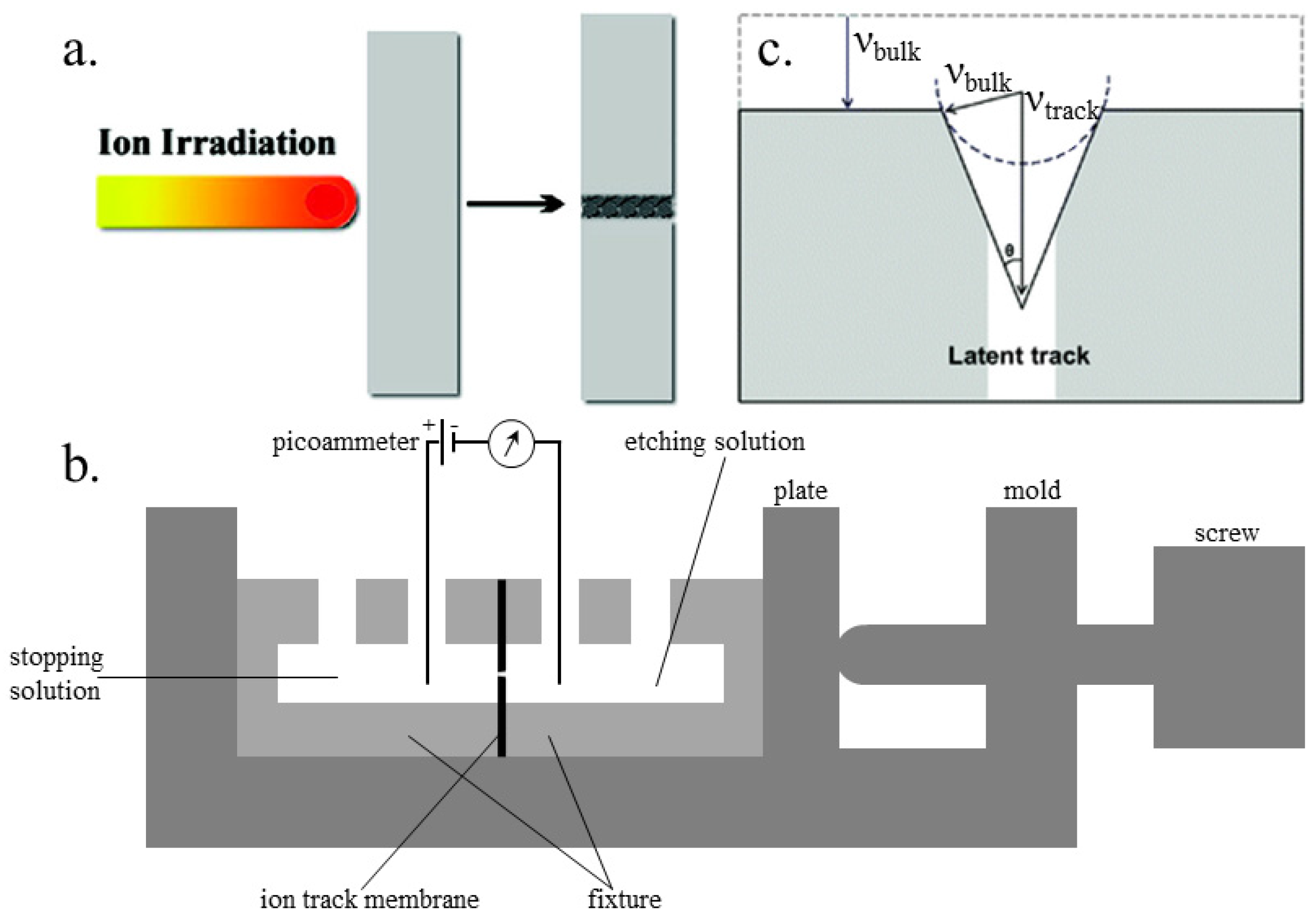
2.1.1. Ion Track-Etching Method
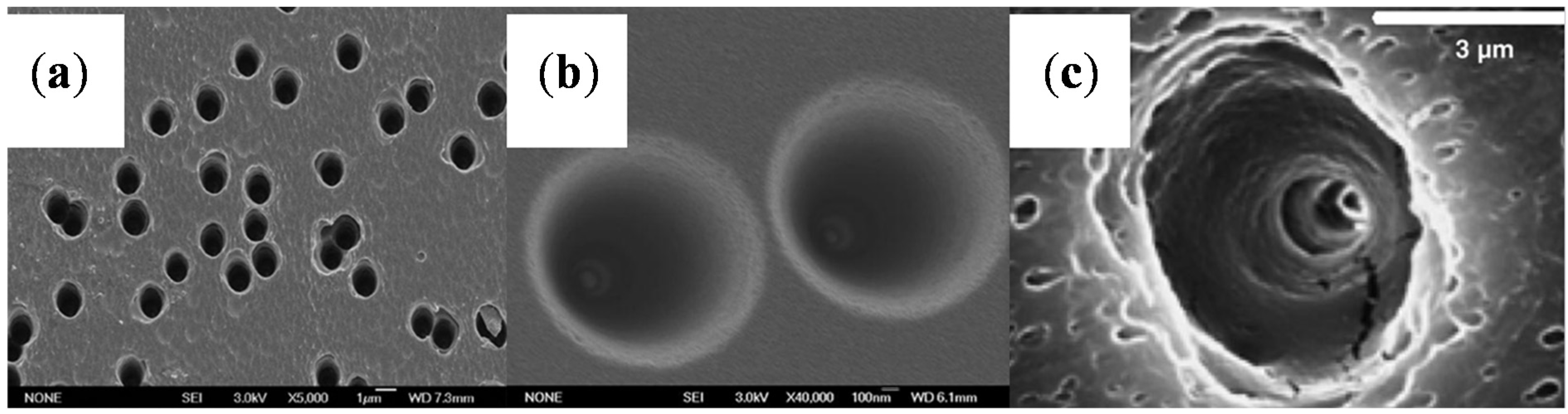
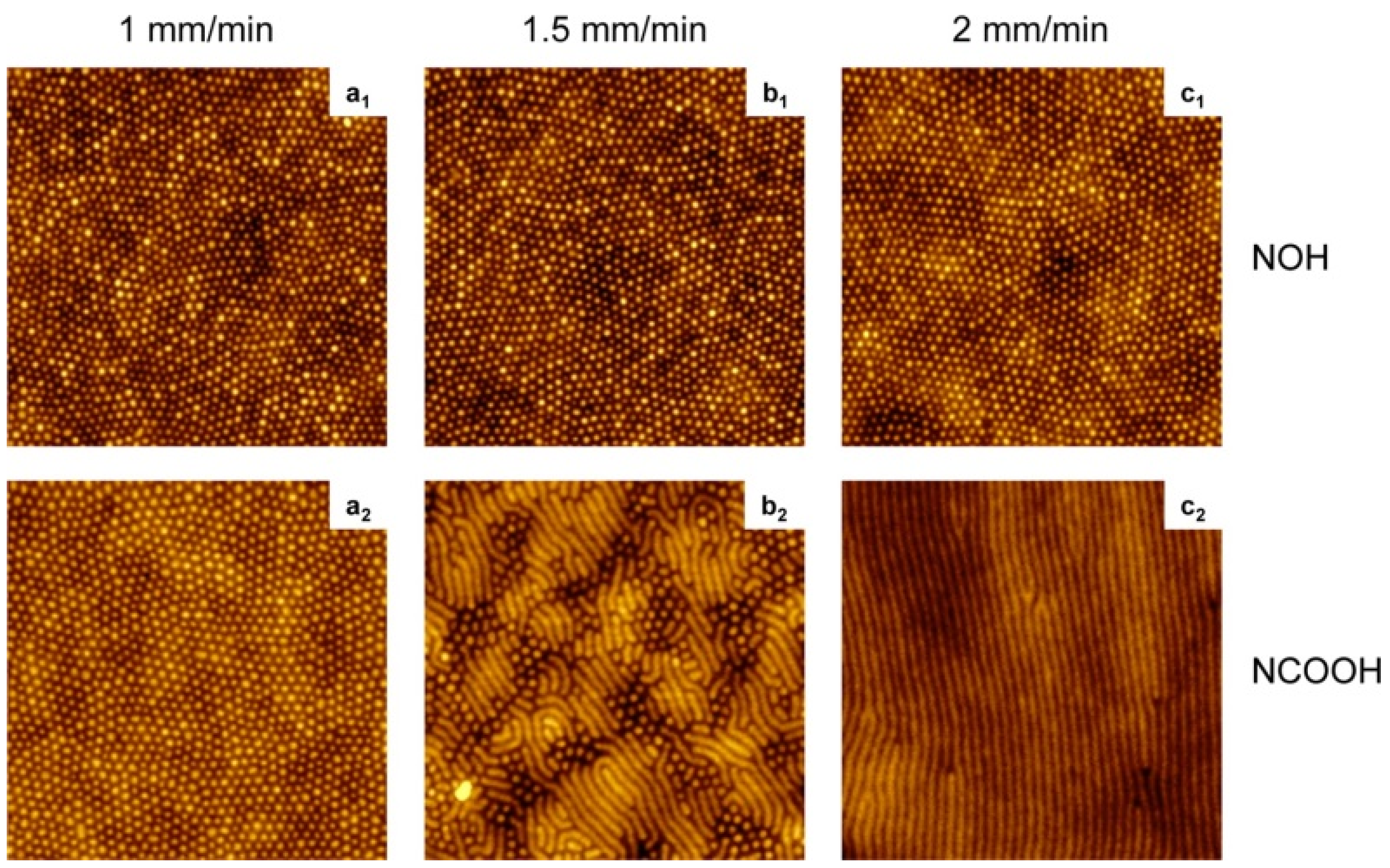
2.1.2. Fabrication of Nanochannels in Different Polymer Membranes

| Polymer | Etchant | Stopping Solution | Temperature | Reference |
|---|---|---|---|---|
| PET (Conical shape) | 9 M NaOH | 1 M KCl or mixture of 2 M KCl and 2 M HCOOH (1:1 by volume) | ~23 °C | [60,61] |
| PI (Conical shape) | NaClO solution of initially high pH value (12.6) with an active chlorine content of 13% | 1 M KI | 50 °C | [61,62,63] |
| PC (Cylindrical shape) | 6 M NaOH (both sides) | - | 60 °C | [61,64] |

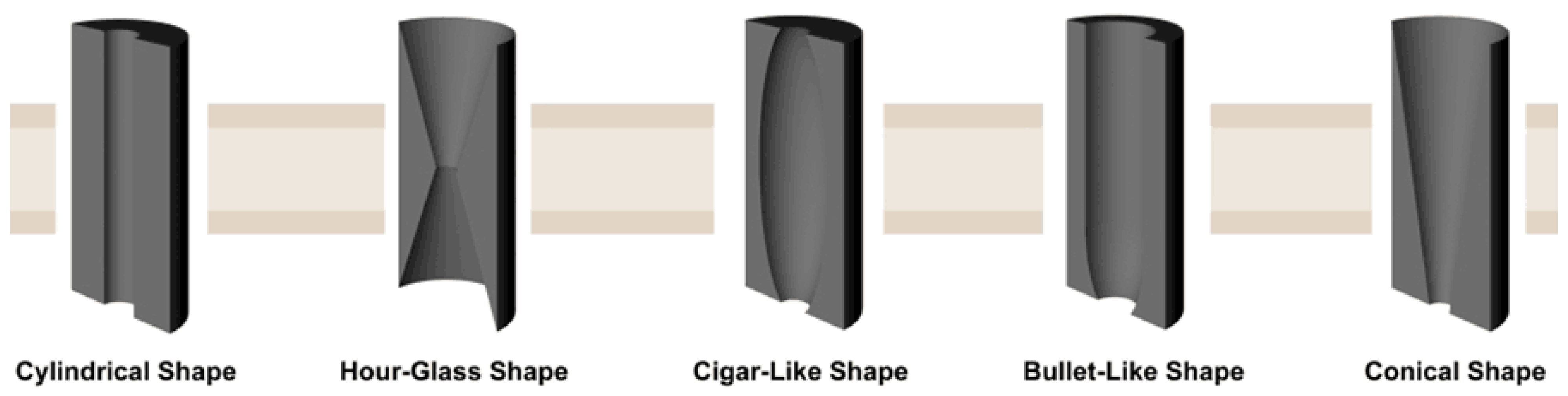
| Shapes | Etchant | Stopping Solution | Temperature | Time | Ref. |
|---|---|---|---|---|---|
| Cylindrical | 2 NaOH (Both sides) | - | 50 °C | 4 min | [68,69,70] |
| Hour-Glass | 9 NaOH (Both sides) | - | ~23 °C | - | [52,71,72,73] |
| Cigar-Like | 6 M NaOH + 0.025% SDDD a (Both sides) | - | 60 °C | 16 min | [74,75,76] |
| Bullet-Like | 6 M NaOH + 0.05% (w/w) Dowfax 2A1 b | 6 M NaOH | 60 °C | - | [77,78,79] |
| Conical | 9 M NaOH | 1 M KCl + 1 M HCOOH | ~23 °C | - | [60,80,81] |
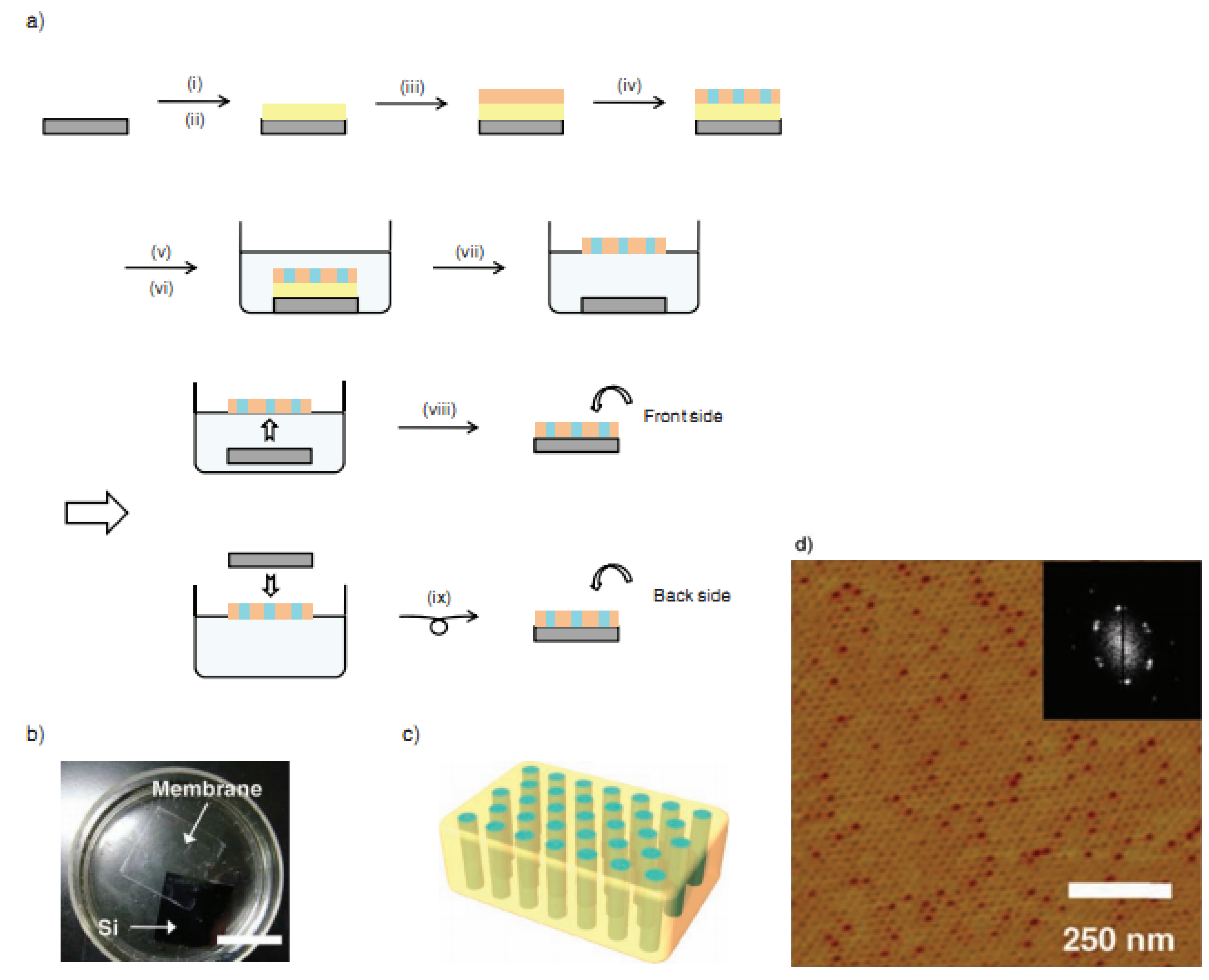
2.1.3. Block Copolymer Self-Assembly Method Based on Phase Separation Processes
2.1.4. Fabrication of Nanochannels Using Different Block Copolymers


2.2. Inorganics
2.2.1. Particle Beam Sputtering Method


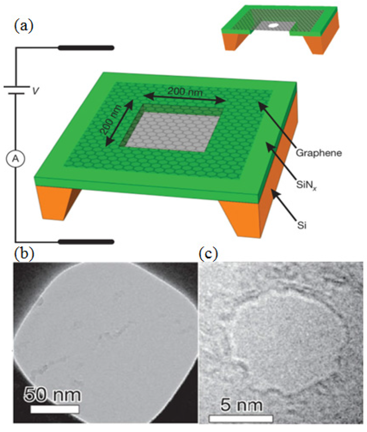
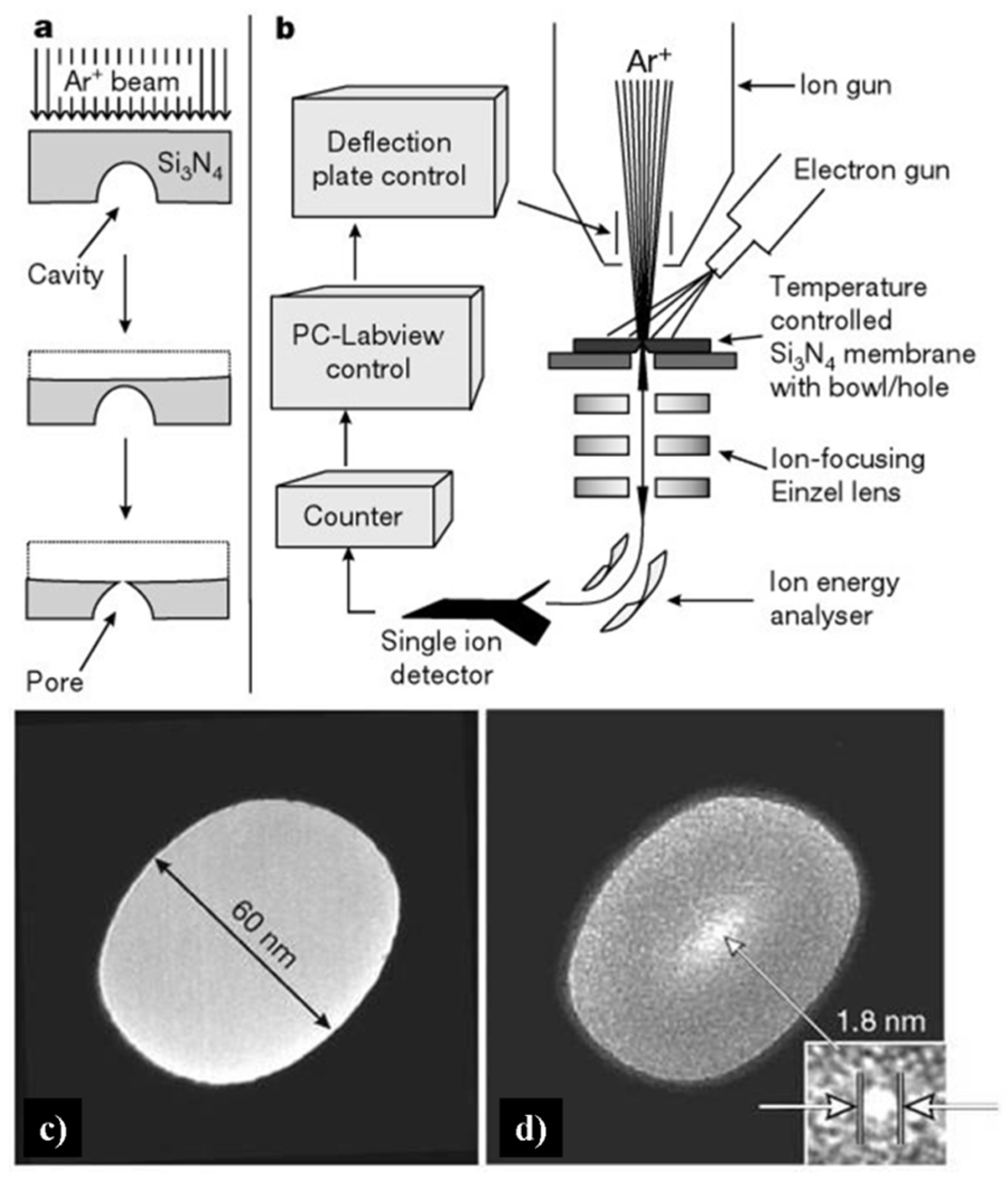
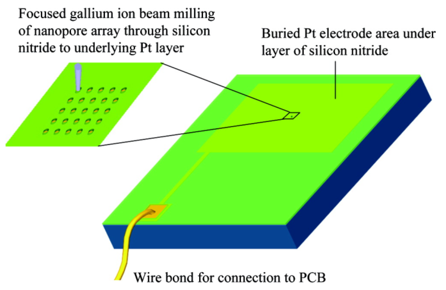
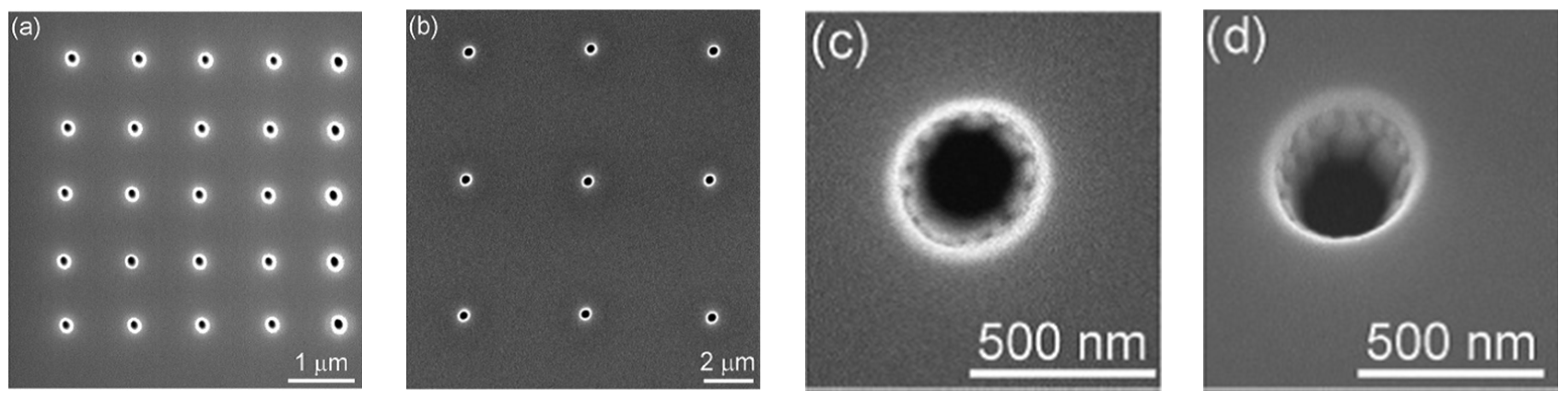
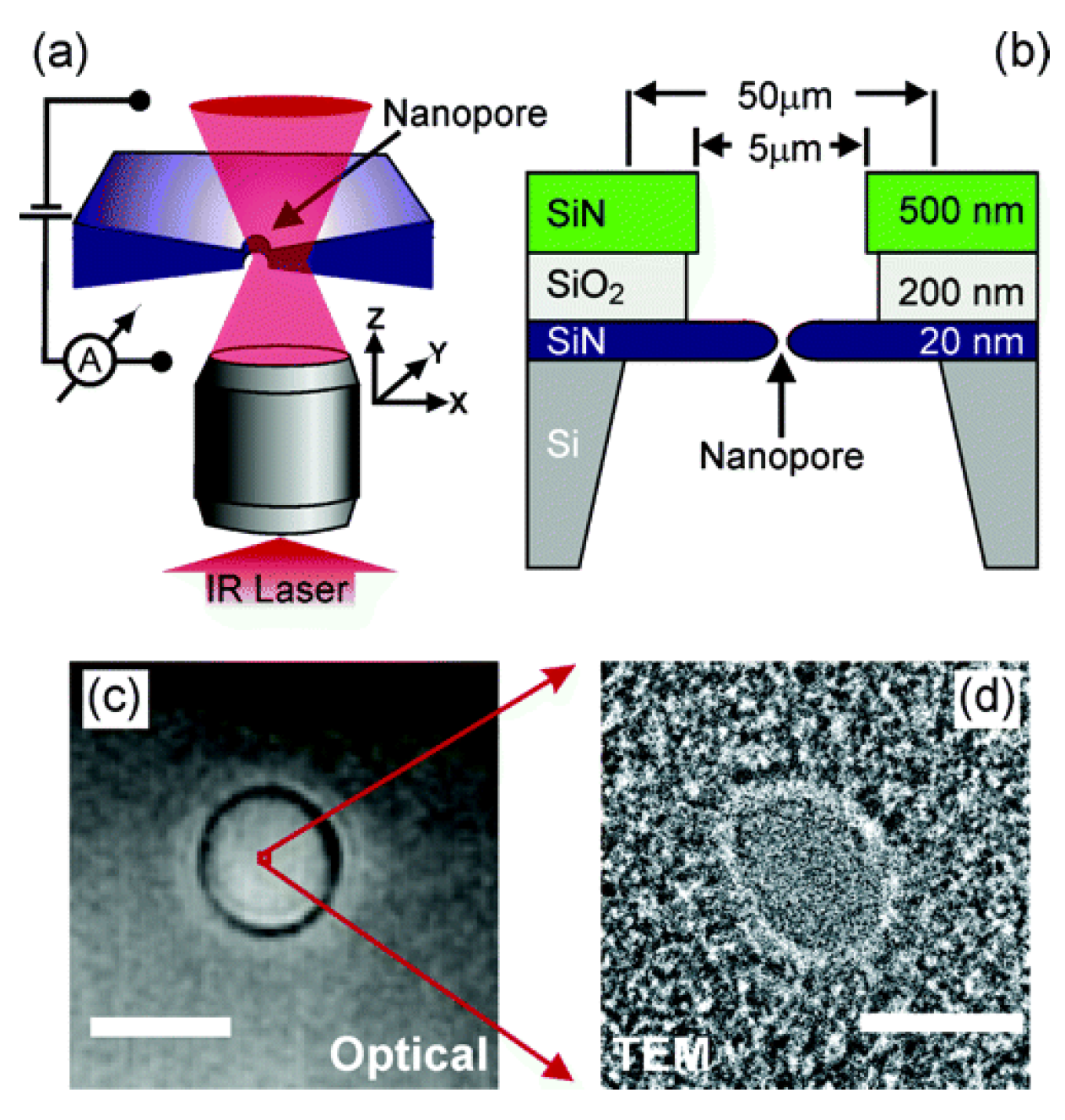
2.2.2. Focused Ion Beam Direct Writing Method (Si3N4)


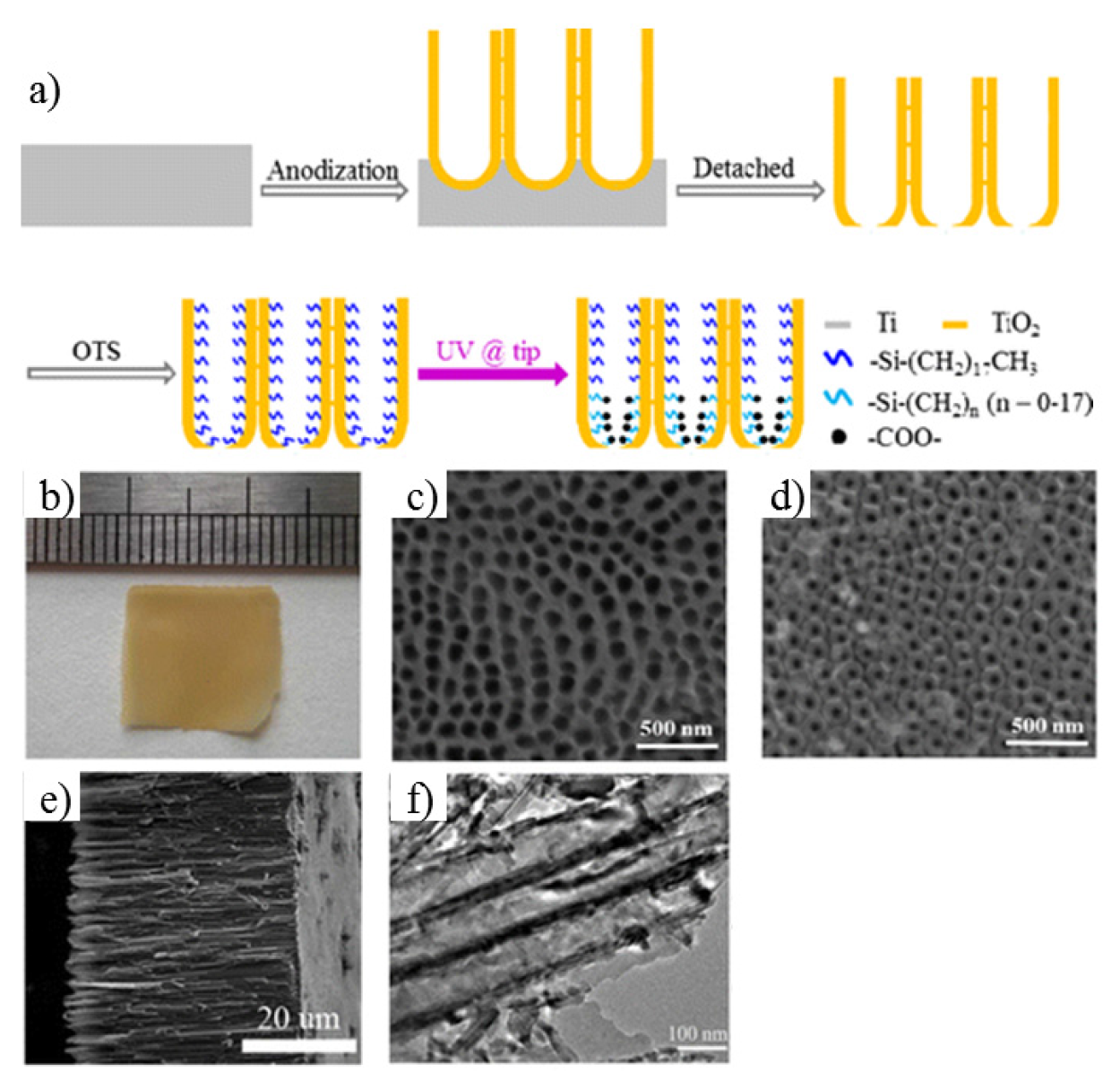
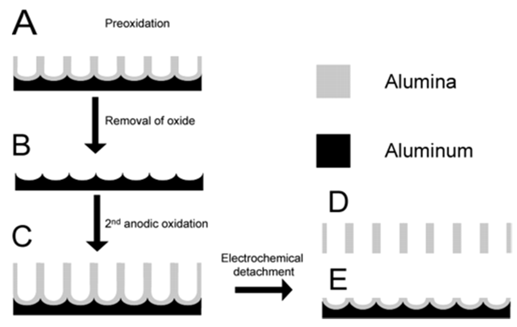
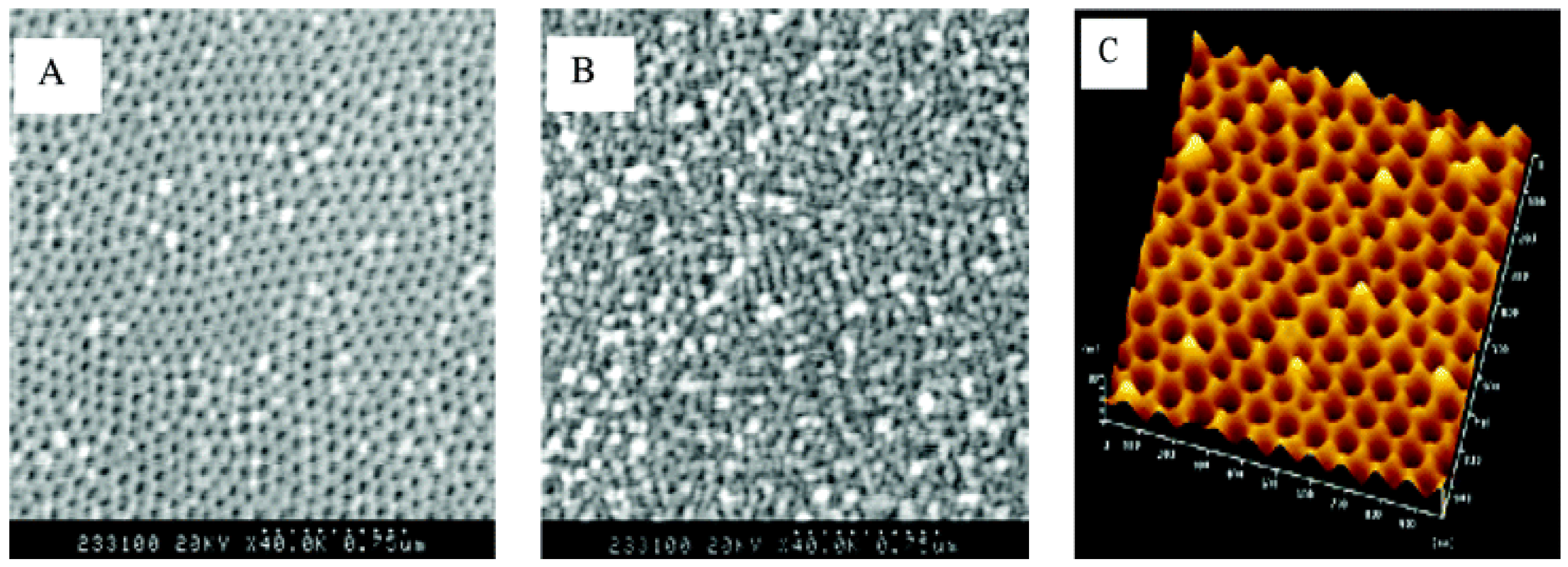
2.2.3. Anodic Oxidation Method


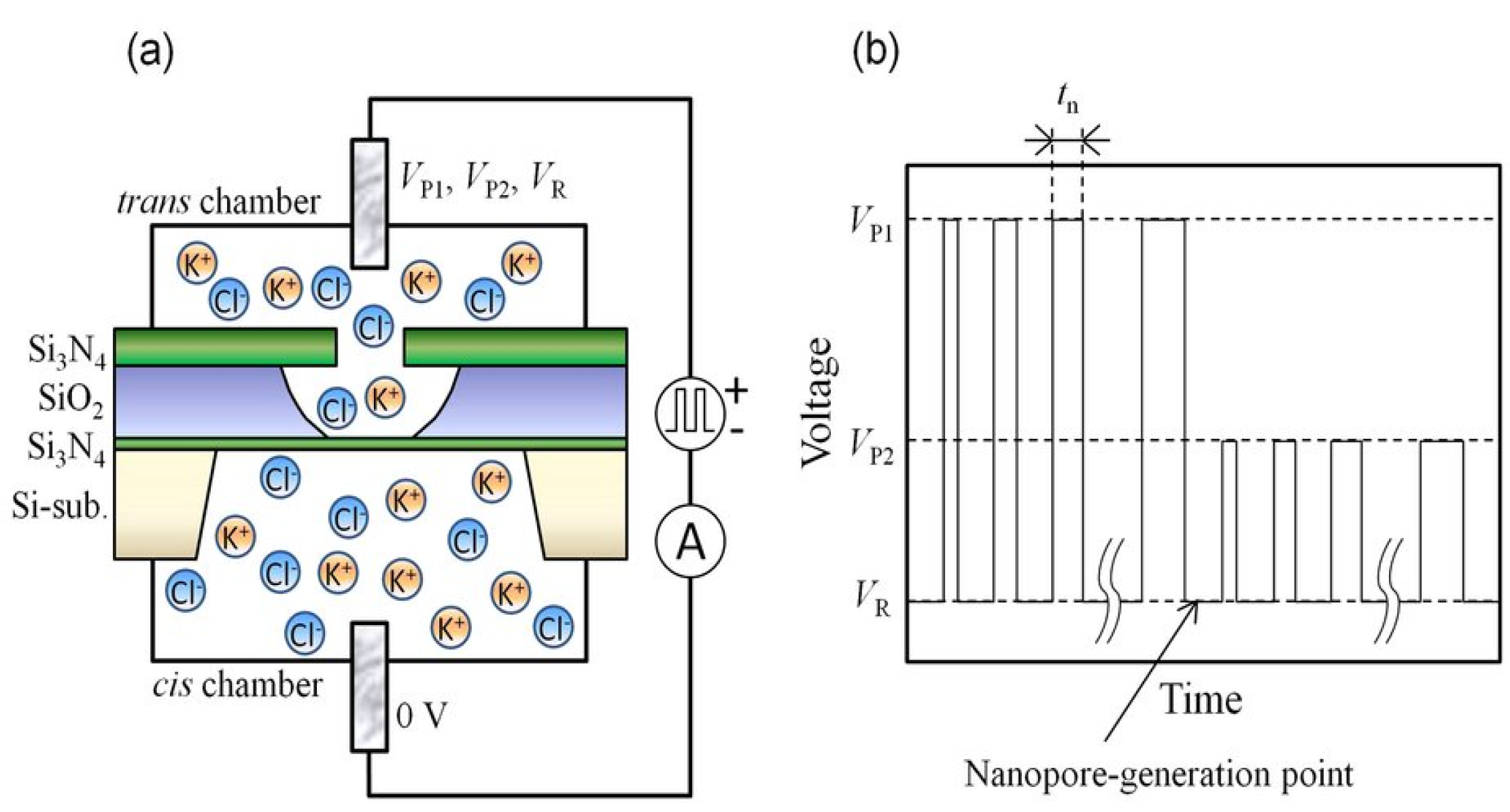
2.2.4. Dielectric Breakdown Method

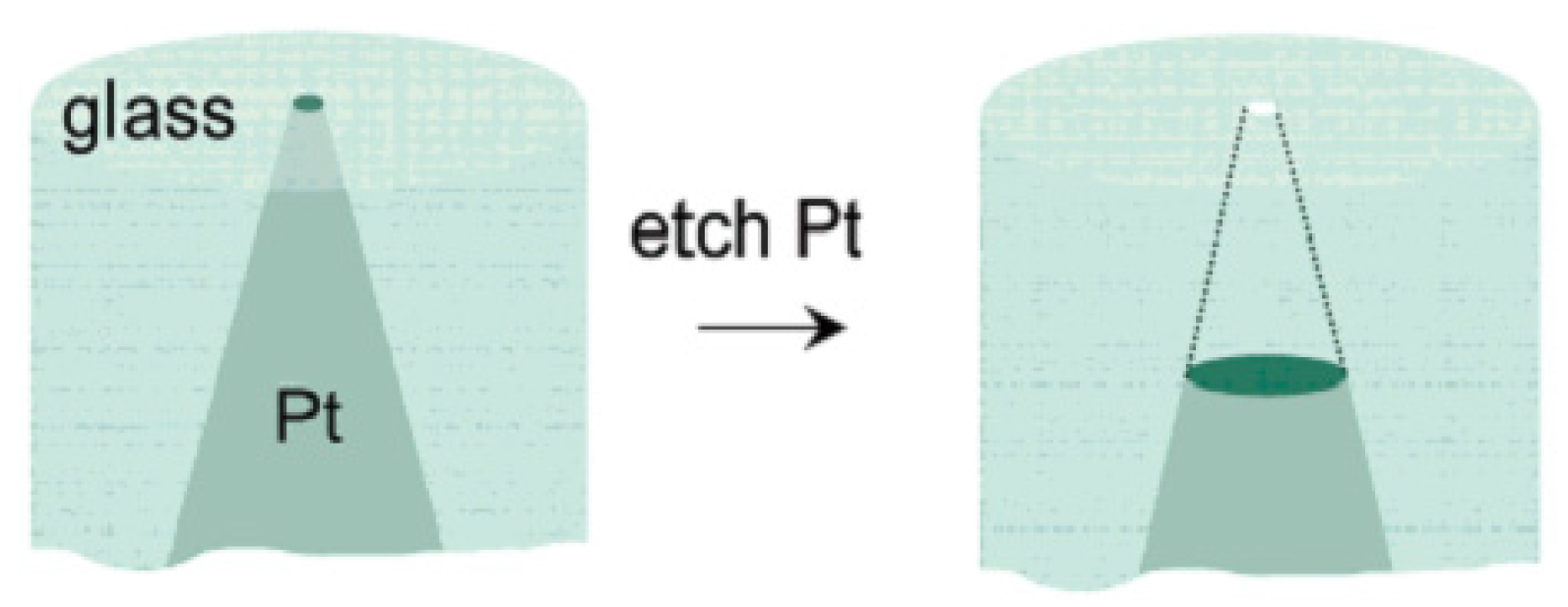
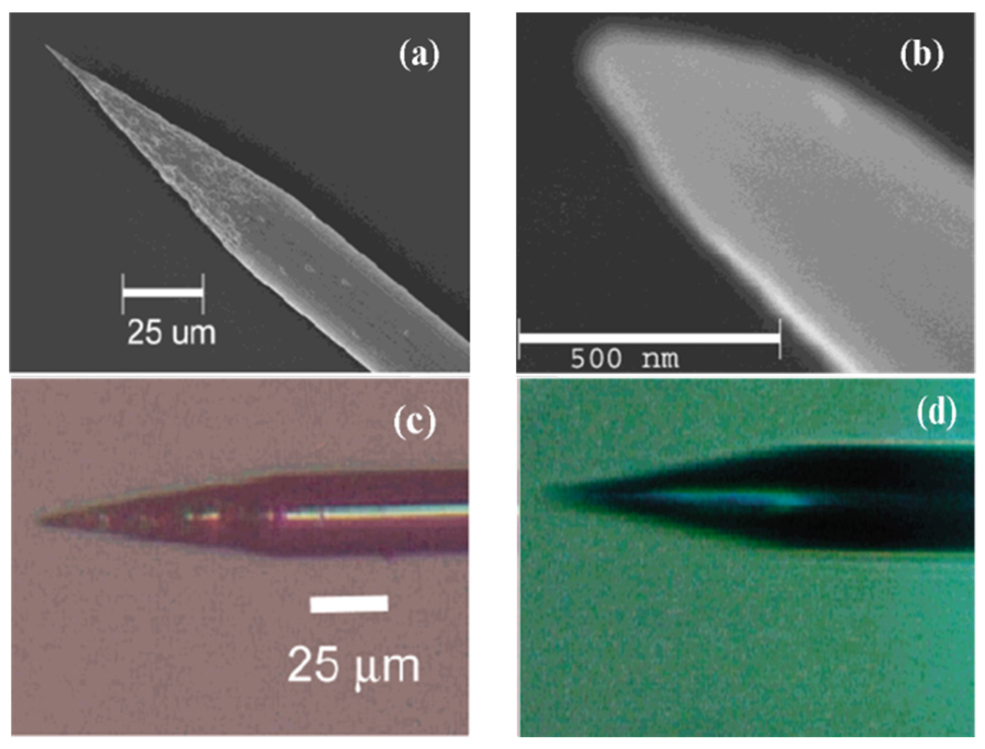
2.2.5. Electrochemical Etching Method (Glass)

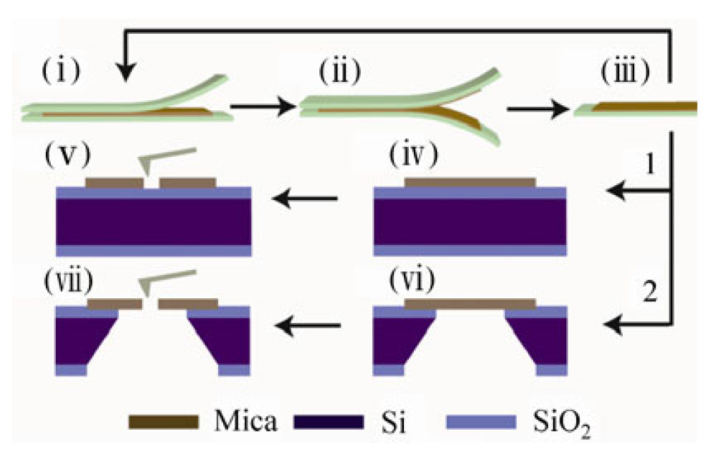
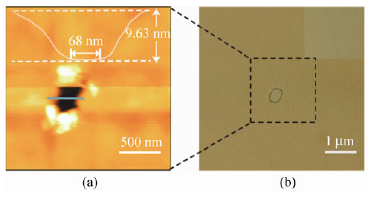
2.2.6. Mechanical Loading Method (Mica)
| Method | Materials | Comments | Ref. |
|---|---|---|---|
| Ion-beam sputtering method | Si3N4 | The method could be useful for fabricating a variety of nanoscale semiconductor devices, as similar sculpting phenomena have been observed for geometries such as thin slits, trenches, and crosses, in several materials like SiO2, Si, and Al. | [74,75] |
| Electron beam etched method | Si/SiO2 | Using the SOI-based process, it is straightforward to obtain this requirement with electron-beam lithography, and should be attainable even with optical lithography alone. | [43,46] |
| Electron beam nanosculpting method | Graphene | Nanometer-scale pores in the graphene were electron-beam-drilled in a 200-keV JEOL 2010 transmission electron microscope. The atomic thinness, stability, and electrical sensitivity of graphene motivate scientists to investigate the potential use of graphene membranes. | [51] |
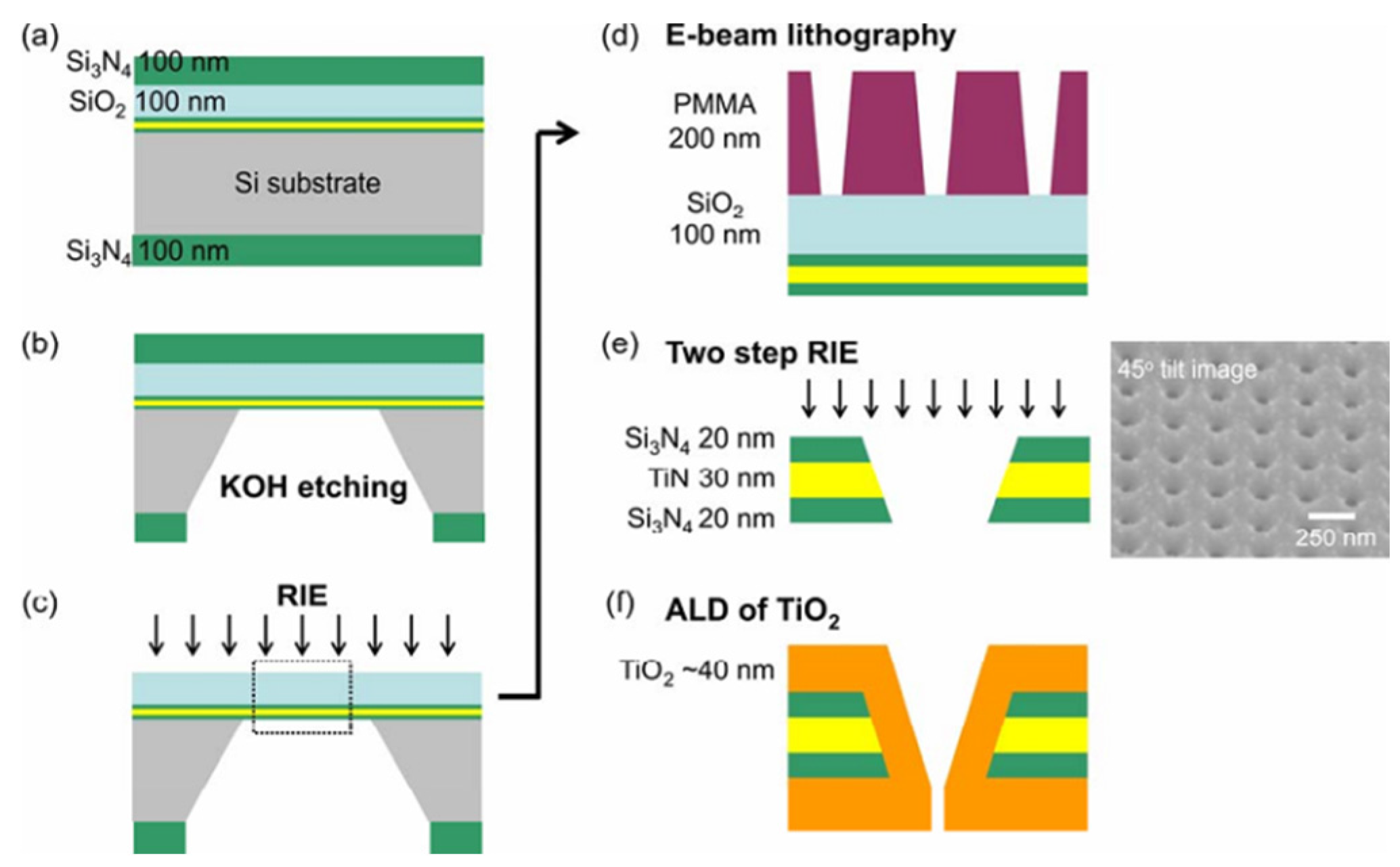
| Focused ion beam direct writing method | Si3N4 | FIB milling has great practical relevance for the fabrication of prototypes and their subsequent experimental evaluation prior to using more prolonged approaches to fabricate the engineered devices. The milling method creates a truncated cone-shaped pore, rather than a cylinder. Thus a model for diffusion-controlled current at a disk electrode at the base of such a truncated cone was developed. | [59] |
| Masuda’s two step anodization process method | Al2O3 | A two-step oxidation process is enough for preparation of well-ordered pores. The present pore-opening process using short electrical oxidation for detaching the porous anodic alumina (PAA) film was used to improve the fabrication of anodic alumina with an array of nanopores. | [64] |
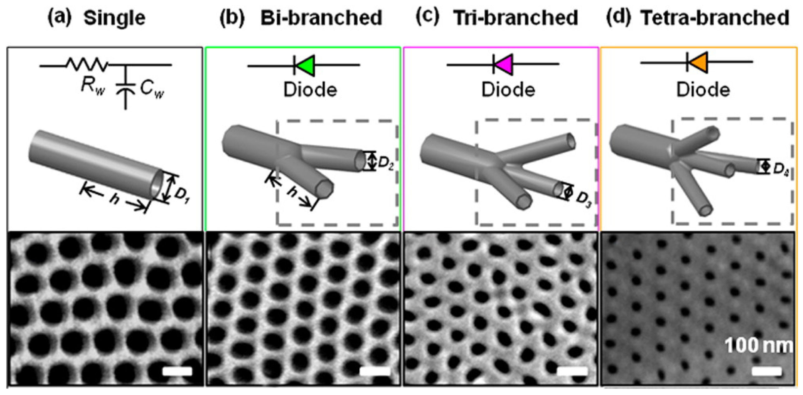
| Electrochemical anodization method | TiO2 | Compared with previous artificial nanochannels, the new type of artificial nanochannel is more facile to fabricate and behaves as a diode that rectifies the ion transport, which also shows some other potential applications such as sensor and separation materials. | [67] |
| Electrochemical etched method | Glass | Electrodes with pore orifice radii less than 100 nm are relatively straightforward to fabricate using equipment and materials commonly found in the laboratory. This will be the topic of a forthcoming publication. | [71] |
| Mechanical loading method | Mica | The fabricated nanopores are geometrically asymmetric, which is like an inverted quadrangular frustum pyramid. The nanopore geometry can be engineered by finely tuning the mechanical load on the AFM tip and the scanning area. It may find potential usage as functional components in nanofluidic devices. | [52] |


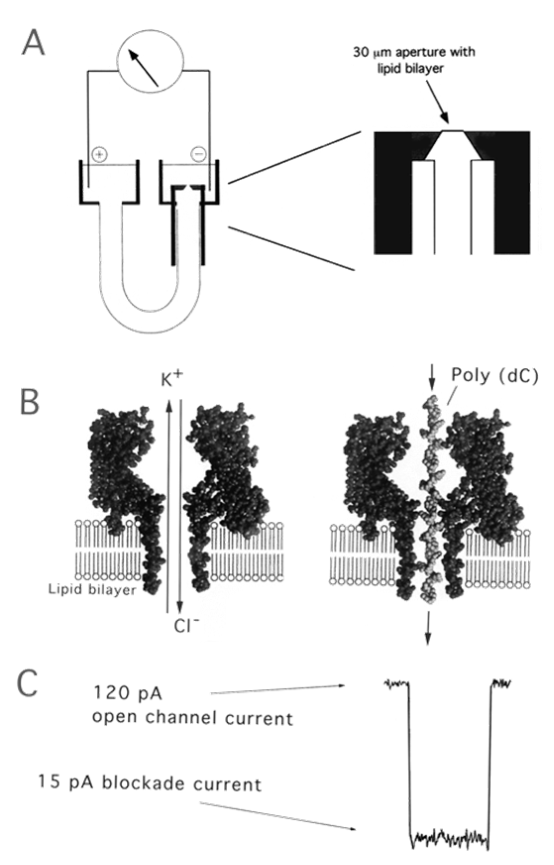
2.3. Biotic Materials
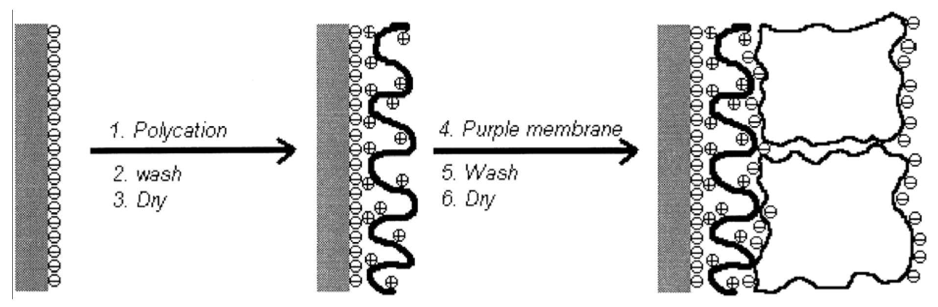
Manual Assembly Method
2.4. Composite Materials
2.4.1. Deposition Etching Method

2.4.2. Reactive Ion Etching (RIE) Method
3. Conclusions and Outlook
Acknowledgments
Author Contributions
Conflicts of Interest
References
- Appenzeller, T. The man who dared to think small. Science 1991, 254, 1300–1301. [Google Scholar] [CrossRef] [PubMed]
- Autumn, K.; Liang, Y.A.; Hsieh, S.T.; Zesch, W.; Chan, W.P.; Kenny, T.W.; Fearing, R.; Full, R.J. Adhesive force of a single gecko foot-hair. Nature 2000, 405, 681–685. [Google Scholar] [PubMed]
- Binnig, G.; Rohrer, H.; Gerber, C.; Weibel, E. Tunneling through a controllable vacuum gap. Appl. Phys. Lett. 1982, 40, 178–180. [Google Scholar] [CrossRef]
- Douglas, T. A bright bio-inspired future. Science 2003, 299, 1192–1192. [Google Scholar] [CrossRef] [PubMed]
- Eigler, D.M.; Schweizer, E.K. Positioning single atoms with a scanning tunnelling microscope. Nature 1990, 344, 524–526. [Google Scholar] [CrossRef]
- Henry, C.R. Catalytic activity of supported nanometer-sized metal clusters. Appl. Surf. Sci. 2000, 164, 252–259. [Google Scholar] [CrossRef]
- Maira, A.J.; Yeung, K.L.; Lee, C.Y.; Yue, P.L.; Chan, C.K. Size effects in gas-phase photo-oxidation of trichloroethylene using nanometer-sized TiO2 catalysts. J. Catal. 2000, 192, 185–196. [Google Scholar] [CrossRef]
- Zhdanov, V.P.; Kasemo, B. Simulations of the reaction kinetics on nanometer supported catalyst particles. Surf. Sci. Rep. 2000, 39, 25–104. [Google Scholar] [CrossRef]
- Hu, L.; Chen, G. Analysis of optical absorption in silicon nanowire arrays for photovoltaic applications. Nano Lett. 2007, 7, 3249–3252. [Google Scholar] [CrossRef] [PubMed]
- Tennakone, K.; Kumara, G.R.R.A.; Kumarasinghe, A.R.; Wijayantha, K.G.U.; Sirimanne, P.M. A dye-sensitized nano-porous solid-state photovoltaic cell. Semicond. Sci. Technol. 1995, 10. [Google Scholar] [CrossRef]
- Yu, J.; Fan, J.; Lv, K. Anatase TiO2 nanosheets with exposed (001) facets: Improved photoelectric conversion efficiency in dye-sensitized solar cells. Nanoscale 2010, 2, 2144–2149. [Google Scholar] [CrossRef] [PubMed]
- Kuil, M.E.; Bodenstaff, E.R.; Hoedemaeker, F.J.; Abrahams, J.P. Protein nano-crystallogenesis. Enzyme Microb. Technol. 2002, 30, 262–265. [Google Scholar] [CrossRef]
- Ruiz, A.; Valsesia, A.; Bretagnol, F.; Colpo, P.; Rossi, F. Large-area protein nano-arrays patterned by soft lithography. Nanotechnology 2007, 18. [Google Scholar] [CrossRef]
- Woo, K.M.; Chen, V.J.; Ma, P.X. Nano-fibrous scaffolding architecture selectively enhances protein adsorption contributing to cell attachment. J. Biomed. Mater. Res. Part A 2003, 67, 531–537. [Google Scholar] [CrossRef] [PubMed]
- Oster, C.G.; Wittmar, M.; Bakowsky, U.; Kissel, T. DNA nano-carriers from biodegradable cationic branched polyesters are formed by a modified solvent displacement method. J. Control. Release 2006, 111, 371–381. [Google Scholar] [CrossRef] [PubMed]
- Reif, J. The design of autonomous DNA nano-mechanical devices: Walking and rolling DNA. Nat. Comput. 2003, 2, 439–461. [Google Scholar] [CrossRef]
- Wang, C.; Huang, Z.; Lin, Y.; Ren, J.; Qu, X. Artificial DNA nano-spring powered by protons. Adv. Mater. 2010, 22, 2792–2798. [Google Scholar] [CrossRef] [PubMed]
- Knez, M.; Sumser, M.; Bittner, A.M.; Wege, C.; Jeske, H.; Kooi, S.; Burghard, M.; Kern, K. Electrochemical modification of individual nano-objects. J. Electroanal. Chem. 2002, 522, 70–74. [Google Scholar] [CrossRef]
- Mertens, P.P.C.; Diprose, J. The bluetongue virus core: A nano-scale transcription machine. Virus Res. 2004, 101, 29–43. [Google Scholar] [CrossRef] [PubMed]
- Feng, L.; Li, S.; Li, Y.; Li, H.; Zhang, L.; Zhai, J.; Song, Y.; Liu, B.; Jiang, L.; Zhu, D. Super-hydrophobic surfaces: From natural to artificial. Adv. Mater. 2002, 14, 1857–1860. [Google Scholar]
- Gao, X.; Jiang, L. Biophysics: Water-repellent legs of water striders. Nature 2004, 432, 36–36. [Google Scholar] [CrossRef] [PubMed]
- Gao, X.; Yan, X.; Yao, X.; Xu, L.; Zhang, K.; Zhang, J.; Yang, B.; Jiang, L. The dry-style antifogging properties of mosquito compound eyes and artificial analogues prepared by soft lithography. Adv. Mater. 2007, 19, 2213–2217. [Google Scholar] [CrossRef]
- Grojean, R.; Sousa, J.; Henry, M. Utilization of solar radiation by polar animals: An optical model for pelts. Appl. Opt. 1980, 19, 339–346. [Google Scholar] [CrossRef] [PubMed]
- Liu, M.; Wang, S.; Wei, Z.; Song, Y.; Jiang, L. Bioinspired design of a superoleophobic and low adhesive water/solid interface. Adv. Mater. 2009, 21, 665–669. [Google Scholar] [CrossRef]
- Mayer, G. Rigid biological systems as models for synthetic composites. Science 2005, 310, 1144–1147. [Google Scholar] [CrossRef] [PubMed]
- Parker, A.R.; Lawrence, C.R. Water capture by a desert beetle. Nature 2001, 414, 33–34. [Google Scholar] [CrossRef] [PubMed]
- Sun, T.; Feng, L.; Gao, X.; Jiang, L. Bioinspired surfaces with special wettability. Acc. Chem. Res. 2005, 38, 644–652. [Google Scholar] [CrossRef] [PubMed]
- Wang, S.; Feng, L.; Jiang, L. One-step solution-immersion process for the fabrication of stable bionic superhydrophobic surfaces. Adv. Mater. 2006, 18, 767–770. [Google Scholar] [CrossRef]
- Zhu, Y.; Hu, D.; Wan, M.; Jiang, L.; Wei, Y. Conducting and superhydrophobic rambutan-like hollow spheres of polyaniline. Adv. Mater. 2007, 19, 2092–2096. [Google Scholar] [CrossRef]
- Ali, M.; Nguyen, Q.H.; Neumann, R.; Ensinger, W. ATP-modulated ionic transport through synthetic nanochannels. Chem. Commun. 2010, 46, 6690–6692. [Google Scholar] [CrossRef] [PubMed]
- Baker, L.A.; Bird, S.P. Nanopores: A makeover for membranes. Nat. Nanotechnol. 2008, 3, 73–74. [Google Scholar] [CrossRef] [PubMed]
- Baughman, R.H.; Zakhidov, A.A.; de Heer, W.A. Carbon nanotubes-the route toward applications. Science 2002, 297, 787–792. [Google Scholar] [CrossRef] [PubMed]
- Heins, E.A.; Siwy, Z.S.; Baker, L.A.; Martin, C.R. Detecting single porphyrin molecules in a conically shaped synthetic nanopore. Nano Lett. 2005, 5, 1824–1829. [Google Scholar] [CrossRef] [PubMed]
- Kawano, R.; Osaki, T.; Sasaki, H.; Takinoue, M.; Yoshizawa, S.; Takeuchi, S. Rapid detection of a cocaine-binding aptamer using biological nanopores on a chip. J. Am. Chem. Soc. 2011, 133, 8474–8477. [Google Scholar] [CrossRef] [PubMed]
- Liu, H.; He, J.; Tang, J.; Liu, H.; Pang, P.; Cao, D.; Krstic, P.; Joseph, S.; Lindsay, S.; Nuckolls, C. Translocation of single-stranded DNA through single-walled carbon nanotubes. Science 2010, 327, 64–67. [Google Scholar] [CrossRef] [PubMed]
- Maglia, G.; Restrepo, M.R.; Mikhailova, E.; Bayley, H. Enhanced translocation of single DNA molecules through α-hemolysin nanopores by manipulation of internal charge. Proc. Nat. Acad. Sci. USA 2008, 105, 19720–19725. [Google Scholar] [CrossRef] [PubMed]
- Majd, S.; Yusko, E.C.; Billeh, Y.N.; Macrae, M.X.; Yang, J.; Mayer, M. Applications of biological pores in nanomedicine, sensing, and nanoelectronics. Curr. Opin. Biotechnol. 2010, 21, 439–476. [Google Scholar] [CrossRef] [PubMed]
- Mara, A.; Siwy, Z.; Trautmann, C.; Wan, J.; Kamme, F. An asymmetric polymer nanopore for single molecule detection. Nano Lett. 2004, 4, 497–501. [Google Scholar] [CrossRef]
- Osaki, T.; Suzuki, H.; Le Pioufle, B.; Takeuchi, S. Multichannel simultaneous measurements of single-molecule translocation in α-hemolysin nanopore array. Anal. Chem. 2009, 81, 9866–9870. [Google Scholar] [CrossRef] [PubMed]
- Savariar, E.N.; Krishnamoorthy, K.; Thayumanavan, S. Molecular discrimination inside polymer nanotubules. Nat. Nanotechnol. 2008, 3, 112–117. [Google Scholar] [CrossRef] [PubMed]
- Strano, M.S.; Dyke, C.A.; Usrey, M.L.; Barone, P.W.; Allen, M.J.; Shan, H.; Kittrell, C.; Hauge, R.H.; Tour, J.M.; Smalley, R.E. Electronic structure control of single-walled carbon nanotube functionalization. Science 2003, 301, 1519–1522. [Google Scholar] [CrossRef] [PubMed]
- Wang, G.; Bohaty, A.K.; Zharov, I.; White, H.S. Photon gated transport at the glass nanopore electrode. J. Am. Chem. Soc. 2006, 128, 13553–13558. [Google Scholar] [CrossRef] [PubMed]
- Wang, G.; Zhang, B.; Wayment, J.R.; Harris, J.M.; White, H.S. Electrostatic-gated transport in chemically modified glass nanopore electrodes. J. Am. Chem. Soc. 2006, 128, 7679–7686. [Google Scholar] [CrossRef] [PubMed]
- Wen, L.; Jiang, L. Bio-inspired smart gating nanochannels based on polymer films. Sci. China Chem. 2011, 54, 1537–1546. [Google Scholar] [CrossRef]
- Zeng, L.; Yang, Z.; Zhang, H.; Hou, X.; Tian, Y.; Yang, F.; Zhou, J.; Li, L.; Jiang, L. Tunable ionic transport control inside a bio-inspired constructive bi-channel nanofluidic device. Small 2014, 10, 793–801. [Google Scholar] [CrossRef] [PubMed]
- Wen, L.; Jiang, L. Construction of biomimetic smart nanochannels for confined water. Natl. Sci. Rev. 2014, 1, 144–156. [Google Scholar] [CrossRef]
- Guo, W.; Xia, H.; Cao, L.; Xia, F.; Wang, S.; Zhang, G.; Song, Y.; Wang, Y.; Jiang, L.; Zhu, D. Integrating ionic gate and rectifier within one solid-state nanopore via modification with dual-responsive copolymer brushes. Adv. Funct. Mater. 2010, 20, 3561–3567. [Google Scholar] [CrossRef]
- Hou, G.; Peng, Z.; Tian, Y.; Zhang, H.; Jiang, L. Applications of polymer single nanochannels in biosensors. Chin. Sci. Bull. 2013, 58, 1473–1482. [Google Scholar] [CrossRef]
- Hou, X.; Dong, H.; Zhu, D.; Jiang, L. Fabrication of stable single nanochannels with controllable ionic rectification. Small 2010, 6, 361–365. [Google Scholar] [CrossRef] [PubMed]
- Hou, X.; Guo, W.; Xia, F.; Nie, F.Q.; Dong, H.; Tian, Y.; Wen, L.; Wang, L.; Cao, L.; Yang, Y.; et al. A biomimetic potassium responsive nanochannel: G-quadruplex DNA conformational switching in a synthetic nanopore. J. Am. Chem. Soc. 2009, 131, 7800–7805. [Google Scholar] [CrossRef] [PubMed]
- Hou, X.; Jiang, L. Learning from nature: Building bio-inspired smart nanochannels. ACS Nano 2009, 3, 3339–3342. [Google Scholar] [CrossRef] [PubMed]
- Hou, X.; Yang, F.; Li, L.; Song, Y.; Jiang, L.; Zhu, D. A biomimetic asymmetric responsive single nanochannel. J. Am. Chem. Soc. 2010, 132, 11736–11742. [Google Scholar] [CrossRef] [PubMed]
- Tian, Y.; Hou, X.; Jiang, L. Biomimetic ionic rectifier systems: Asymmetric modification of single nanochannels by ion sputtering technology. J. Electroanal. Chem. 2011, 656, 231–236. [Google Scholar] [CrossRef]
- Tian, Y.; Hou, X.; Wen, L.; Guo, W.; Song, Y.; Sun, H.; Wang, Y.; Jiang, L.; Zhu, D. A biomimetic zinc activated ion channel. Chem. Commun. 2010, 46, 1682. [Google Scholar] [CrossRef] [PubMed]
- Wen, L.; Hou, X.; Tian, Y.; Zhai, J.; Jiang, L. Bio-inspired photoelectric conversion based on smart-gating nanochannels. Adv.Funct. Mater. 2010, 20, 2636–2642. [Google Scholar] [CrossRef]
- Wen, L.; Liu, Q.; Ma, J.; Tian, Y.; Li, C.; Bo, Z.; Jiang, L. Malachite green derivative-functionalized single nanochannel: Light-and-pH dual-driven ionic gating. Adv. Mater. 2012, 24, 6193–6198. [Google Scholar] [CrossRef] [PubMed]
- Wen, L.; Ma, J.; Tian, Y.; Zhai, J.; Jiang, L. A photo-induced, and chemical-driven, smart-gating nanochannel. Small 2012, 8, 838–842. [Google Scholar] [CrossRef] [PubMed]
- Xia, F.; Guo, W.; Mao, Y.; Hou, X.; Xue, J.; Xia, H.; Wang, L.; Song, Y.; Ji, H.; Ouyang, Q.; et al. Gating of single synthetic nanopores by proton-driven DNA molecular motors. J. Am. Chem. Soc. 2008, 130, 8345–8350. [Google Scholar] [CrossRef] [PubMed]
- Spohr, R. Real-time control of track etching and recent experiments relevant to micro and nano fabrication. Radiat. Meas. 2008, 43, 560–570. [Google Scholar] [CrossRef]
- Apel, P.Y.; Korchev, Y.E.; Siwy, Z.; Spohr, R.; Yoshida, M. Diode-like single-ion track membrane prepared by electro-stopping. Nucl. Instrum. Methods Phys. Res. Sect. B 2001, 184, 337–346. [Google Scholar] [CrossRef]
- Wen, L.; Tian, Y.; Ma, J.; Zhai, J.; Jiang, L. Construction of biomimetic smart nanochannels with polymer membranes and application in energy conversion systems. Phys. Chem. Chem. Phys. 2012, 14, 4027–4042. [Google Scholar] [CrossRef] [PubMed]
- Trautmann, C.; Brüchle, W.; Spohr, R.; Vetter, J.; Angert, N. Pore geometry of etched ion tracks in polyimide. Nucl. Instrum. Methods Phys. Res. Sect. B 1996, 111, 70–74. [Google Scholar] [CrossRef]
- Siwy, Z.; Dobrev, D.; Neumann, R.; Trautmann, C.; Voss, K. Electro-responsive asymmetric nanopores in polyimide with stable ion-current signal. Appl. Phys. A 2003, 76, 781–785. [Google Scholar] [CrossRef]
- Apel’, P.Y.; Blonskaya, I.V.; Orelovich, O.L.; Akimenko, S.N.; Sartowska, B.; Dmitriev, S.N. Factors determining pore shape in polycarbonate track membranes. Colloid J. 2004, 66, 649–656. [Google Scholar] [CrossRef]
- Tian, Y.; Zhang, Z.; Wen, L.; Ma, J.; Zhang, Y.; Liu, W.; Zhai, J.; Jiang, L. A biomimetic mercury(II)-gated single nanochannel. Chem. Commun. 2013, 49, 10679–10681. [Google Scholar] [CrossRef] [PubMed]
- Harrell, C.C.; Siwy, Z.S.; Martin, C.R. Conical nanopore membranes: Controlling the nanopore shape. Small 2006, 2, 194–198. [Google Scholar] [CrossRef] [PubMed]
- Hou, X.; Zhang, H.; Jiang, L. Building bio-inspired artificial functional nanochannels: From symmetric to asymmetric modification. Angew. Chem. Int. Ed. 2012, 51, 5296–5307. [Google Scholar] [CrossRef] [PubMed]
- Ali, M.; Ramirez, P.; Tahir, M.N.; Mafe, S.; Siwy, Z.; Neumann, R.; Tremel, W.; Ensinger, W. Biomolecular conjugation inside synthetic polymer nanopores via glycoprotein-lectin interactions. Nanoscale 2011, 3, 1894–1903. [Google Scholar] [CrossRef] [PubMed]
- Kovalev, Y.S.; Levkovich, N.V.; Kuklin, A.I.; Apel’, P.Y. Surfactant aggregation in solutions applied for track etching and its possible effect on the pore shape in track membranes. Colloid J. 2009, 71, 634–639. [Google Scholar] [CrossRef]
- Pevarnik, M.; Healy, K.; Toimil-Molares, M.E.; Morrison, A.; Létant, S.E.; Siwy, Z.S. Polystyrene particles reveal pore substructure as they translocate. ACS Nano 2012, 6, 7295–7302. [Google Scholar] [CrossRef] [PubMed]
- Gillespie, D.; Boda, D.; He, Y.; Apel, P.; Siwy, Z.S. Synthetic nanopores as a test case for ion channel theories: The anomalous mole fraction effect without single filing. Biophys. J. 2008, 95, 609–619. [Google Scholar] [CrossRef] [PubMed]
- Kalman, E.B.; Vlassiouk, I.; Siwy, Z.S. Nanofluidic bipolar transistors. Adv. Mater. 2008, 20, 293–297. [Google Scholar] [CrossRef]
- Hou, X.; Liu, Y.; Dong, H.; Yang, F.; Li, L.; Jiang, L. A pH-gating ionic transport nanodevice: Asymmetric chemical modification of single nanochannels. Adv. Mater. 2010, 22, 2440–2443. [Google Scholar] [CrossRef] [PubMed]
- Ali, M.; Ramirez, P.; Nguyen, H.Q.; Nasir, S.; Cervera, J.; Mafe, S.; Ensinger, W. Single cigar-shaped nanopores functionalized with amphoteric amino acid chains: Experimental and theoretical characterization. ACS Nano 2012, 6, 3631–3640. [Google Scholar] [CrossRef] [PubMed]
- Apel, P.Y.; Blonskaya, I.V.; Didyk, A.Y.; Dmitriev, S.N.; Orelovitch, O.L.; Root, D.; Samoilova, L.I.; Vutsadakis, V.A. Surfactant-enhanced control of track-etch pore morphology. Nucl. Instrum. Methods Phys. Res. Sect. B Beam Int. Mater. At. 2001, 179, 55–62. [Google Scholar] [CrossRef]
- Apel, P.Y.; Blonskaya, I.V.; Dmitriev, S.N.; Mamonova, T.I.; Orelovitch, O.L.; Sartowska, B.; Yamauchi, Y. Surfactant-controlled etching of ion track nanopores and its practical applications in membrane technology. Radiat. Meas. 2008, 43, S552–S559. [Google Scholar] [CrossRef]
- Pavel Yu, A.; Blonskaya, I.V.; Orelovitch, O.L.; Ramirez, P.; Sartowska, B.A. Effect of nanopore geometry on ion current rectification. Nanotechnology 2011, 22, 175302–175314. [Google Scholar]
- Pavel Yu, A.; Irina, V.B.; Sergei, N.D.; Oleg, L.O.; Adam, P.; Bozena, A.S. Fabrication of nanopores in polymer foils with surfactant-controlled longitudinal profiles. Nanotechnology 2007, 18. [Google Scholar] [CrossRef]
- Apel, P.Y.; Blonskaya, I.V.; Orelovitch, O.L.; Dmitriev, S.N. Diode-like ion-track asymmetric nanopores: Some alternative methods of fabrication. Nucl. Instrum. Methods Phys. Res. Sect. B Beam Int. Mater. At. 2009, 267, 1023–1027. [Google Scholar] [CrossRef]
- Siwy, Z.; Apel, P.; Dobrev, D.; Neumann, R.; Spohr, R.; Trautmann, C.; Voss, K. Ion transport through asymmetric nanopores prepared by ion track etching. Nucl. Instrum. Methods Phys. Res. Sect. B Beam Int. Mater. At. 2003, 208, 143–148. [Google Scholar] [CrossRef]
- Siwy, Z.; Fuliński, A. Fabrication of a synthetic nanopore ion pump. Phys. Rev. Lett. 2002, 89. [Google Scholar] [CrossRef]
- van de Witte, P.; Dijkstra, P.J.; van den Berg, J.W.A.; Feijen, J. Phase separation processes in polymer solutions in relation to membrane formation. J. Membr. Sci. 1996, 117, 1–31. [Google Scholar] [CrossRef]
- Xu, H.; Goedel, W.A. Polymer-silica hybrid monolayers as precursors for ultrathin free-standing porous membranes. Langmuir 2002, 18, 2363–2367. [Google Scholar] [CrossRef]
- Tang, Z.; Kotov, N.A.; Magonov, S.; Ozturk, B. Nanostructured artificial nacre. Nat. Mater. 2003, 2, 413–418. [Google Scholar] [CrossRef] [PubMed]
- Nardin, C.; Winterhalter, M.; Meier, W. Giant free-standing ABA triblock copolymer membranes. Langmuir 2000, 16, 7708–7712. [Google Scholar] [CrossRef]
- Markutsya, S.; Jiang, C.; Pikus, Y.; Tsukruk, V.V. Freely suspended layer-by-layer nanomembranes: Testing micromechanical properties. Adv. Funct. Mater. 2005, 15, 771–780. [Google Scholar] [CrossRef]
- Mamedov, A.A.; Kotov, N.A.; Prato, M.; Guldi, D.M.; Wicksted, J.P.; Hirsch, A. Molecular design of strong single-wall carbon nanotube/polyelectrolyte multilayer composites. Nat. Mater. 2002, 1, 190–194. [Google Scholar] [CrossRef] [PubMed]
- Yamamoto, T.; Kimura, T.; Komura, M.; Suzuki, Y.; Iyoda, T.; Asaoka, S.; Nakanishi, H. Block copolymer permeable membrane with visualized high-density straight channels of poly(ethylene oxide). Adv. Funct. Mater. 2011, 21, 918–926. [Google Scholar] [CrossRef]
- Mansky, P.; Liu, Y.; Huang, E.; Russell, T.P.; Hawker, C. Controlling polymer-surface interactions with random copolymer brushes. Science 1997, 275, 1458–1460. [Google Scholar] [CrossRef]
- Lewis, F.D.; Bedell, A.M.; Dykstra, R.E.; Elbert, J.E.; Gould, I.R.; Farid, S. Photochemical generation, isomerization, and oxygenation of stilbene cation radicals. J. Am. Chem. Soc. 1990, 112, 8055–8064. [Google Scholar] [CrossRef]
- Shichi, T.; Takagi, K.; Sawaki, Y. Stereoselectivity control of [2 + 2] photocycloaddition by changing site distances of hydrotalcite interlayers. Chem. Commun. 1996. [Google Scholar] [CrossRef]
- Krins, N.; Faustini, M.; Louis, B.; Grosso, D. Thick and crack-free nanocrystalline mesoporous TiO2 films obtained by capillary coating from aqueous solutions. Chem. Mater. 2010, 22, 6218–6220. [Google Scholar] [CrossRef]
- Roland, S.; Prud’homme, R.E.; Bazuin, C.G. Morphology, thickness, and composition evolution in supramolecular block copolymer films over a wide range of dip-coating rates. ACS Macro Lett. 2012, 1, 973–976. [Google Scholar] [CrossRef]
- Grosso, D. How to exploit the full potential of the dip-coating process to better control film formation. J. Mater. Chem. 2011, 21, 17033–17038. [Google Scholar] [CrossRef]
- Böker, A.; Müller, A.H.E.; Krausch, G. Nanoscopic surface patterns from functional ABC triblock copolymers. Macromolecules 2001, 34, 7477–7488. [Google Scholar] [CrossRef]
- Mamedov, A.A.; Kotov, N.A. Free-standing layer-by-layer assembled films of magnetite nanoparticles. Langmuir 2000, 16, 5530–5533. [Google Scholar] [CrossRef]
- Mallwitz, F.; Laschewsky, A. Direct access to stable, freestanding polymer membranes by layer-by-layer assembly of polyelectrolytes. Adv. Mater. 2005, 17, 1296–1299. [Google Scholar] [CrossRef]
- Jiang, C.; Markutsya, S.; Tsukruk, V.V. Compliant, robust, and truly nanoscale free-standing multilayer films fabricated using spin-assisted layer-by-layer assembly. Adv. Mater. 2004, 16, 157–161. [Google Scholar] [CrossRef]
- Huck, W.T.S.; Stroock, A.D.; Whitesides, G.M. Synthesis of geometrically well defined, molecularly thin polymer films. Angew. Chem. Int. Ed. 2000, 39, 1058–1061. [Google Scholar] [CrossRef]
- Eck, W.; Küller, A.; Grunze, M.; Völkel, B.; Gölzhäuser, A. Freestanding nanosheets from crosslinked biphenyl self-assembled monolayers. Adv. Mater. 2005, 17, 2583–2587. [Google Scholar] [CrossRef]
- Roland, S.; Pellerin, C.; Bazuin, C.G.; Prud’homme, R.E. Evolution of small molecule content and morphology with dip-coating rate in supramolecular PS-P4VP thin films. Macromolecules 2012, 45, 7964–7972. [Google Scholar] [CrossRef]
- Li, J.; Stein, D.; McMullan, C.; Branton, D.; Aziz, M.J.; Golovchenko, J.A. Ion-beam sculpting at nanometre length scales. Nature 2001, 412, 166–169. [Google Scholar] [CrossRef] [PubMed]
- Ziegler, J.F.; Biersack, J.P. The Stopping and Range of Ions in Matter. 1985. Available online: http://www.srim.org/SRIM/SRIMINTRO.htm (accessed on 15 September 2015).
- Wang, D.; Harrer, S.; Luan, B.; Stolovitzky, G.; Peng, H.; Afzali-Ardakani, A. Regulating the transport of DNA through biofriendly nanochannels in a thin solid membrane. Sci. Rep. 2014, 4. [Google Scholar] [CrossRef] [PubMed]
- Storm, A.J.; Chen, J.H.; Ling, X.S.; Zandbergen, H.W.; Dekker, C. Fabrication of solid-state nanopores with single-nanometre precision. Nat. Mater. 2003, 2, 537–540. [Google Scholar] [CrossRef] [PubMed]
- Gribov, N.; Theeuwen, S.; Caro, J.; Radelaar, S. A new fabrication process for metallic point contacts. Microelectron. Eng. 1997, 35, 317–320. [Google Scholar] [CrossRef]
- Chen, G.S.; Boothroyd, C.B.; Humphreys, C.J. Novel fabrication method for nanometer-scale silicon dots and wires. Appl. Phys. Lett. 1993, 62, 1949–1951. [Google Scholar] [CrossRef]
- Chen, G.S.; Boothroyd, C.B.; Humphreys, C.J. Electron-beam-induced damage in amorphous SiO2 and the direct fabrication of silicon nanostructures. Philos. Mag. A 1998, 78, 491–506. [Google Scholar] [CrossRef]
- Kasianowicz, J.J.; Brandin, E.; Branton, D.; Deamer, D.W. Characterization of individual polynucleotide molecules using a membrane channel. Proc. Natl. Acad. Sci. USA 1996, 93, 13770–13773. [Google Scholar] [CrossRef] [PubMed]
- Taylor, G.; Michael, D. On making holes in a sheet of fluid. J. Fluid Mech. 1973, 58, 625–639. [Google Scholar] [CrossRef]
- Garaj, S.; Hubbard, W.; Reina, A.; Kong, J.; Branton, D.; Golovchenko, J.A. Graphene as a subnanometre trans-electrode membrane. Nature 2010, 467, 190–193. [Google Scholar] [CrossRef] [PubMed]
- Reina, A.; Jia, X.; Ho, J.; Nezich, D.; Son, H.; Bulovic, V.; Dresselhaus, M.S.; Kong, J. Large area, few-layer graphene films on arbitrary substrates by chemical vapor deposition. Nano Lett. 2008, 9, 30–35. [Google Scholar] [CrossRef] [PubMed]
- Reina, A.; Thiele, S.; Jia, X.; Bhaviripudi, S.; Dresselhaus, M.; Schaefer, J.; Kong, J. Growth of large-area single- and Bi-layer graphene by controlled carbon precipitation on polycrystalline Ni surfaces. Nano Res. 2009, 2, 509–516. [Google Scholar] [CrossRef]
- Fischbein, M.D.; Drndić, M. Electron beam nanosculpting of suspended graphene sheets. Appl. Phys. Lett. 2008, 93. [Google Scholar] [CrossRef]
- Garaj, S.; Liu, S.; Golovchenko, J.A.; Branton, D. Molecule-hugging graphene nanopores. Proc. Natl. Acad. Sci. USA 2013, 110, 12192–12196. [Google Scholar] [CrossRef] [PubMed]
- Liu, Y.; Dong, X.; Chen, P. Biological and chemical sensors based on graphene materials. Chem. Soc. Rev. 2012, 41, 2283–2307. [Google Scholar] [CrossRef] [PubMed]
- Schneider, G.G.F.; Kowalczyk, S.W.; Calado, V.E.; Pandraud, G.G.; Zandbergen, H.W.; Vandersypen, L.M.K.; Dekker, C. DNA translocation through graphene nanopores. NANO Lett. 2010, 10, 3163–3167. [Google Scholar] [CrossRef] [PubMed]
- Venkatesan, B.M.; Bashir, R. Nanopore sensors for nucleic acid analysis. Nat. Nanotechnol. 2011, 6, 615–624. [Google Scholar] [CrossRef] [PubMed]
- Liu, K.; Feng, J.; Kis, A.; Radenovic, A. Atomically thin molybdenum disulfide nanopores with high sensitivity for DNA translocation. ACS Nano 2014, 8, 2504–2511. [Google Scholar] [CrossRef] [PubMed]
- Liu, S.; Lu, B.; Zhao, Q.; Li, J.; Gao, T.; Chen, Y.; Zhang, Y.; Liu, Z.; Fan, Z.; Yang, F.; et al. Boron nitride nanopores: Highly sensitive DNA single-molecule detectors. Adv. Mater. 2013, 25, 4549–4554. [Google Scholar] [CrossRef] [PubMed]
- Zhou, Z.; Hu, Y.; Wang, H.; Xu, Z.; Wang, W.; Bai, X.; Shan, X.; Lu, X. DNA translocation through hydrophilic nanopore in hexagonal boron nitride. Sci. Rep. 2013, 3. [Google Scholar] [CrossRef] [PubMed]
- Tseng, A.A. Recent developments in nanofabrication using focused ion beams. Small 2005, 1, 924–939. [Google Scholar] [CrossRef] [PubMed]
- Lanyon, Y.H.; De Marzi, G.; Watson, Y.E.; Quinn, A.J.; Gleeson, J.P.; Redmond, G.; Arrigan, D.W. Fabrication of nanopore array electrodes by focused ion beam milling. Anal. Chem. 2007, 79, 3048–3055. [Google Scholar] [CrossRef] [PubMed]
- Kim, M.J.; Wanunu, M.; Bell, D.C.; Meller, A. Rapid fabrication of uniformly sized nanopores and nanopore arrays for parallel DNA analysis. Adv. Mater. 2006, 18, 3149–3153. [Google Scholar] [CrossRef]
- Dela Torre, R.; Larkin, J.; Singer, A.; Meller, A. Fabrication and characterization of solid-state nanopore arrays for high-throughput DNA sequencing. Nanotechnology 2012, 23. [Google Scholar] [CrossRef] [PubMed]
- Eftekhari, F.; Escobedo, C.; Ferreira, J.; Duan, X.; Girotto, E.M.; Brolo, A.G.; Gordon, R.; Sinton, D. Nanoholes as nanochannels: Flow-through plasmonic sensing. Anal. Chem. 2009, 81, 4308–4311. [Google Scholar] [CrossRef] [PubMed]
- Yuan, J.H.; He, F.Y.; Sun, D.C.; Xia, X.H. A simple method for preparation of through-hole porous anodic alumina membrane. Chem. Mater. 2004, 16, 1841–1844. [Google Scholar] [CrossRef]
- Masuda, H.; Fukuda, K. Ordered metal nanohole arrays made by a two-step replication of honeycomb structures of anodic alumina. Science 1995, 268, 1466–1468. [Google Scholar] [CrossRef] [PubMed]
- Li, C.Y.; Ma, F.X.; Wu, Z.Q.; Gao, H.L.; Shao, W.T.; Wang, K.; Xia, X.H. Solution-pH-modulated rectification of ionic current in highly ordered nanochannel arrays patterned with chemical functional groups at designed positions. Adv. Funct. Mater. 2013, 23, 3836–3844. [Google Scholar] [CrossRef]
- Vlassiouk, I.; Takmakov, P.; Smirnov, S. Sensing DNA hybridization via ionic conductance through a nanoporous electrode. Langmuir 2005, 21, 4776–4778. [Google Scholar] [CrossRef] [PubMed]
- Yan, R.; Liang, W.; Fan, R.; Yang, P. Nanofluidic diodes based on nanotube heterojunctions. Nano Lett. 2009, 9, 3820–3825. [Google Scholar] [CrossRef] [PubMed]
- Kong, Y.; Fan, X.; Zhang, M.; Hou, X.; Liu, Z.; Zhai, J.; Jiang, L. Nanofluidic diode based on branched alumina nanochannels with tunable ionic rectification. ACS Appl. Mater. Interfaces 2013, 5, 7931–7936. [Google Scholar] [CrossRef] [PubMed]
- Chen, B.; Xu, Q.; Zhao, X.; Zhu, X.; Kong, M.; Meng, G. Branched silicon nanotubes and metal nanowires via AAO-template-assistant approach. Adv. Funct. Mater. 2010, 20, 3791–3796. [Google Scholar] [CrossRef]
- Hu, Z.; Zhang, Q.; Gao, J.; Liu, Z.; Zhai, J.; Jiang, L. Photocatalysis-triggered ion rectification in artificial nanochannels based on chemically modified asymmetric TiO2 Nanotubes. Langmuir 2013, 29, 4806–4812. [Google Scholar] [CrossRef] [PubMed]
- Chen, Q.; Xu, D. Large-scale, noncurling, and free-standing crystallized TiO2 nanotube arrays for dye-sensitized solar cells. J. Phys. Chem. C 2009, 113, 6310–6314. [Google Scholar] [CrossRef]
- Mor, G.K.; Shankar, K.; Paulose, M.; Varghese, O.K.; Grimes, C.A. Enhanced photocleavage of water using titania nanotube arrays. Nano Lett. 2004, 5, 191–195. [Google Scholar] [CrossRef] [PubMed]
- Zhang, Q.; Liu, Z.; Hou, X.; Fan, X.; Zhai, J.; Jiang, L. Light-regulated ion transport through artificial ion channels based on TiO2 nanotubular arrays. Chem. Commun. 2012, 48, 5901–5903. [Google Scholar] [CrossRef] [PubMed]
- Yanagi, I.; Akahori, R.; Hatano, T.; Takeda, K.I. Fabricating nanopores with diameters of sub-1 nm to 3 nm using multilevel pulse-voltage injection. Sci. Rep. 2014, 4. [Google Scholar] [CrossRef] [PubMed]
- Briggs, K.; Kwok, H.; Tabard-Cossa, V. Automated fabrication of 2-nm solid-state nanopores for nucleic acid analysis. Small 2014, 10, 2077–2086. [Google Scholar] [CrossRef] [PubMed]
- Kuan, A.T.; Lu, B.; Xie, P.; Szalay, T.; Golovchenko, J.A. Electrical pulse fabrication of graphene nanopores in electrolyte solution. Appl. Phys. Lett. 2015, 106. [Google Scholar] [CrossRef] [PubMed]
- Zhang, B.; Zhang, Y.; White, H.S. The Nanopore Electrode. Anal. Chem. 2004, 76, 6229–6238. [Google Scholar] [CrossRef] [PubMed]
- Melmed, A.J. The art and science and other aspects of making sharp tips. J. Vac. Sci. Technol. B 1991, 9, 601–608. [Google Scholar] [CrossRef]
- Melmed, A.J.; Carroll, J.J. An approach to realism in field ion microscopy via zone electropolishing. J. Vac. Sci. Technol. A 1984, 2, 1388–1389. [Google Scholar] [CrossRef]
- Gao, J.; Guo, W.; Geng, H.; Hou, X.; Shuai, Z.; Jiang, L. Layer-by-layer removal of insulating few-layer mica flakes for asymmetric ultra-thin nanopore fabrication. Nano Res. 2012, 5, 99–108. [Google Scholar] [CrossRef]
- Miyake, S. 1 nm deep mechanical processing of muscovite mica by atomic force microscopy. Appl. Phys. Lett. 1995, 67, 2925–2927. [Google Scholar] [CrossRef]
- Song, L.; Hobaugh, M.R.; Shustak, C.; Cheley, S.; Bayley, H.; Gouaux, J.E. Structure of staphylococcal α-hemolysin, a heptameric transmembrane pore. Science 1996, 274, 1859–1865. [Google Scholar] [CrossRef] [PubMed]
- Deamer, D.W.; Branton, D. Characterization of nucleic acids by nanopore analysis. Acc. Chem. Res. 2002, 35, 817–825. [Google Scholar] [CrossRef] [PubMed]
- Haque, F.; Geng, J.; Montemagno, C.; Guo, P. Incorporation of a viral DNA-packaging motor channel in lipid bilayers for real-time, single-molecule sensing of chemicals and double-stranded DNA. Nat. Protoc. 2013, 8, 373–392. [Google Scholar] [CrossRef] [PubMed]
- Wendell, D.; Jing, P.; Geng, J.; Subramaniam, V.; Lee, T.J.; Montemagno, C.; Guo, P. Translocation of double-stranded DNA through membrane-adapted phi29 motor protein nanopores. Nat. Nanotechnol. 2009, 4, 765–772. [Google Scholar] [CrossRef] [PubMed]
- Liu, L.; Yang, C.; Zhao, K.; Li, J.; Wu, H.C. Ultrashort single-walled carbon nanotubes in a lipid bilayer as a new nanopore sensor. Nat. Commun. 2013, 4. [Google Scholar] [CrossRef] [PubMed]
- He, J.A.; Samuelson, L.; Li, L.; Kumar, J.; Tripathy, S.K. Oriented bacteriorhodopsin/polycation multilayers by electrostatic layer-by-layer assembly. Langmuir 1998, 14, 1674–1679. [Google Scholar] [CrossRef]
- He, J.A.; Samuelson, L.; Li, L.; Kumar, J.; Tripathy, S.K. Photoelectric properties of oriented bacteriorhodopsin/polycation multilayers by electrostatic layer-by-layer assembly. J. Phys. Chem. B 1998, 102, 7067–7072. [Google Scholar] [CrossRef]
- Shibata, A.; Yorimitsu, A.; Ikema, H.; Minami, K.; Ueno, S.; Muneyuki, E.; Higuti, T. Photocurrent of purple membrane adsorbed onto a thin polymer film: Action characteristics of the local anesthetics. Colloids Surf. B 2002, 23, 375–382. [Google Scholar] [CrossRef]
- Keyser, U.F.; Krapf, D.; Koeleman, B.N.; Smeets, R.M.M.; Dekker, N.H.; Dekker, C. Nanopore tomography of a laser focus. Nano Lett. 2005, 5, 2253–2256. [Google Scholar] [CrossRef] [PubMed]
- Krapf, D.; Wu, M.Y.; Smeets, R.M.; Zandbergen, H.W.; Dekker, C.; Lemay, S.G. Fabrication and characterization of nanopore-based electrodes with radii down to 2 nm. Nano Lett. 2006, 6, 105–109. [Google Scholar] [CrossRef] [PubMed]
- Nam, S.W.; Rooks, M.J.; Kim, K.B.; Rossnagel, S.M. Ionic field effect transistors with sub-10 nm multiple nanopores. Nano Lett. 2009, 9, 2044–2048. [Google Scholar] [CrossRef] [PubMed]
- Rossnagel, S.M.; Sherman, A.; Turner, F. Plasma-enhanced atomic layer deposition of Ta and Ti for interconnect diffusion barriers. J. Vac. Sci. Technol. B 2000, 18, 2016–2020. [Google Scholar] [CrossRef]
- Venkatesan, B.M.; Estrada, D.; Banerjee, S.; Jin, X.; Dorgan, V.E.; Bae, M.H.; Aluru, N.R.; Pop, E.; Bashir, R. Stacked graphene-Al2O3 nanopore sensors for sensitive detection of DNA and DNA–protein complexes. ACS Nano 2011, 6, 441–450. [Google Scholar] [CrossRef] [PubMed]
- Broers, A.N. Resolution limits of PMMA resist for exposure with 50 kV electrons. J. Electrochem. Soc. 1981, 128, 166–170. [Google Scholar] [CrossRef]
- Rooks, M.J.; Kratschmer, E.; Viswanathan, R.; Katine, J.; Fontana, R.E.; MacDonald, S.A. Low stress development of poly(methylmethacrylate) for high aspect ratio structures. J. Vac. Sci. Technol. B 2002, 20, 2937–2941. [Google Scholar] [CrossRef]
- Wi, J.S.; Lee, H.S.; Lim, K.; Nam, S.W.; Kim, H.M.; Park, S.Y.; Lee, J.J.; Hong, C.D.; Jin, S.; Kim, K.B. Fabrication of silicon nanopillar teradot arrays by electron-beam patterning for nanoimprint molds. Small 2008, 4, 2118–2122. [Google Scholar] [CrossRef] [PubMed]
- Chen, P.; Mitsui, T.; Farmer, D.B.; Golovchenko, J.; Gordon, R.G.; Branton, D. Atomic layer deposition to fine-tune the surface properties and diameters of fabricated nanopores. Nano Lett. 2004, 4, 1333–1337. [Google Scholar] [CrossRef] [PubMed]
© 2015 by the authors; licensee MDPI, Basel, Switzerland. This article is an open access article distributed under the terms and conditions of the Creative Commons Attribution license (http://creativecommons.org/licenses/by/4.0/).
Share and Cite
Zhang, Y.; Kong, X.-Y.; Gao, L.; Tian, Y.; Wen, L.; Jiang, L. Fabrication of Nanochannels. Materials 2015, 8, 6277-6308. https://doi.org/10.3390/ma8095304
Zhang Y, Kong X-Y, Gao L, Tian Y, Wen L, Jiang L. Fabrication of Nanochannels. Materials. 2015; 8(9):6277-6308. https://doi.org/10.3390/ma8095304
Chicago/Turabian StyleZhang, Yuqi, Xiang-Yu Kong, Loujun Gao, Ye Tian, Liping Wen, and Lei Jiang. 2015. "Fabrication of Nanochannels" Materials 8, no. 9: 6277-6308. https://doi.org/10.3390/ma8095304
APA StyleZhang, Y., Kong, X.-Y., Gao, L., Tian, Y., Wen, L., & Jiang, L. (2015). Fabrication of Nanochannels. Materials, 8(9), 6277-6308. https://doi.org/10.3390/ma8095304