
Work Function Adjustment by Using Dipole Engineering for TaN-Al2O3-Si3N4-HfSiOx-Silicon Nonvolatile Memory

Abstract
:1. Introduction
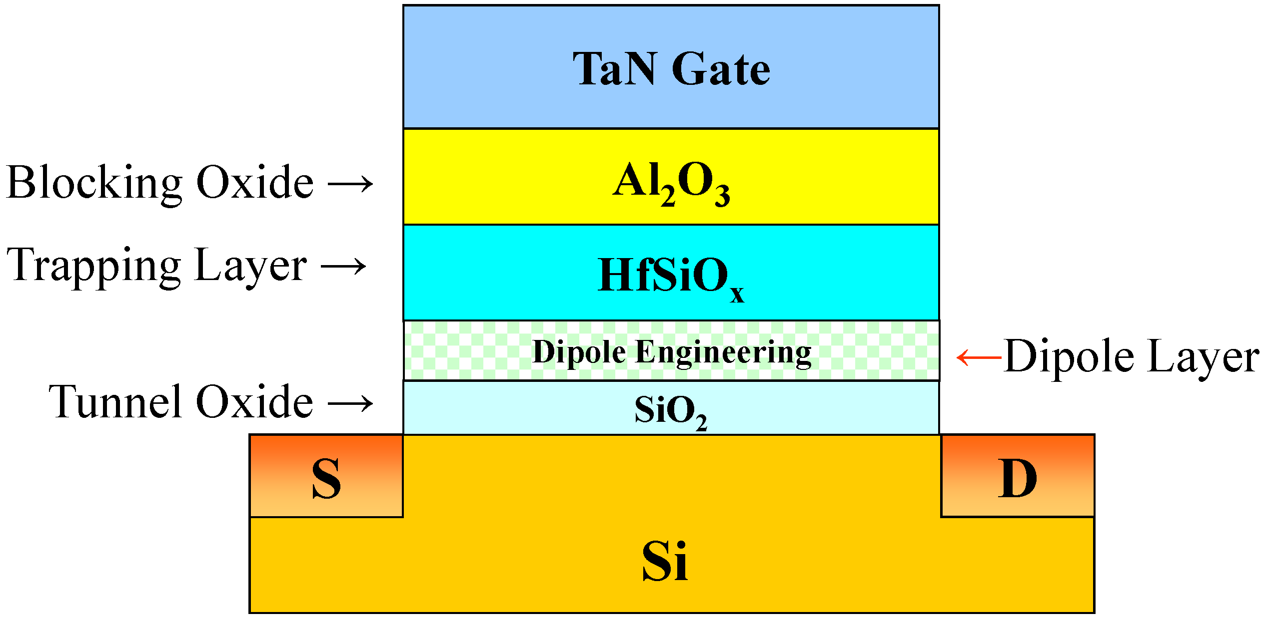
2. Experimental Section

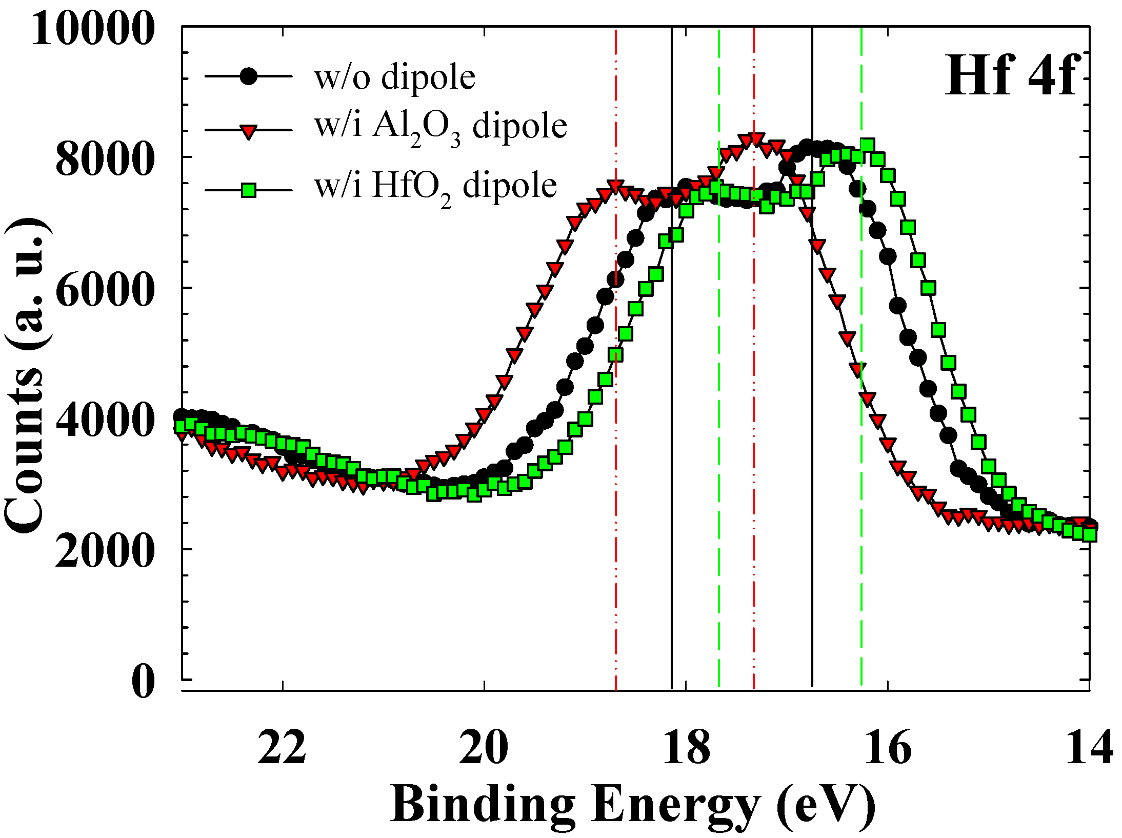
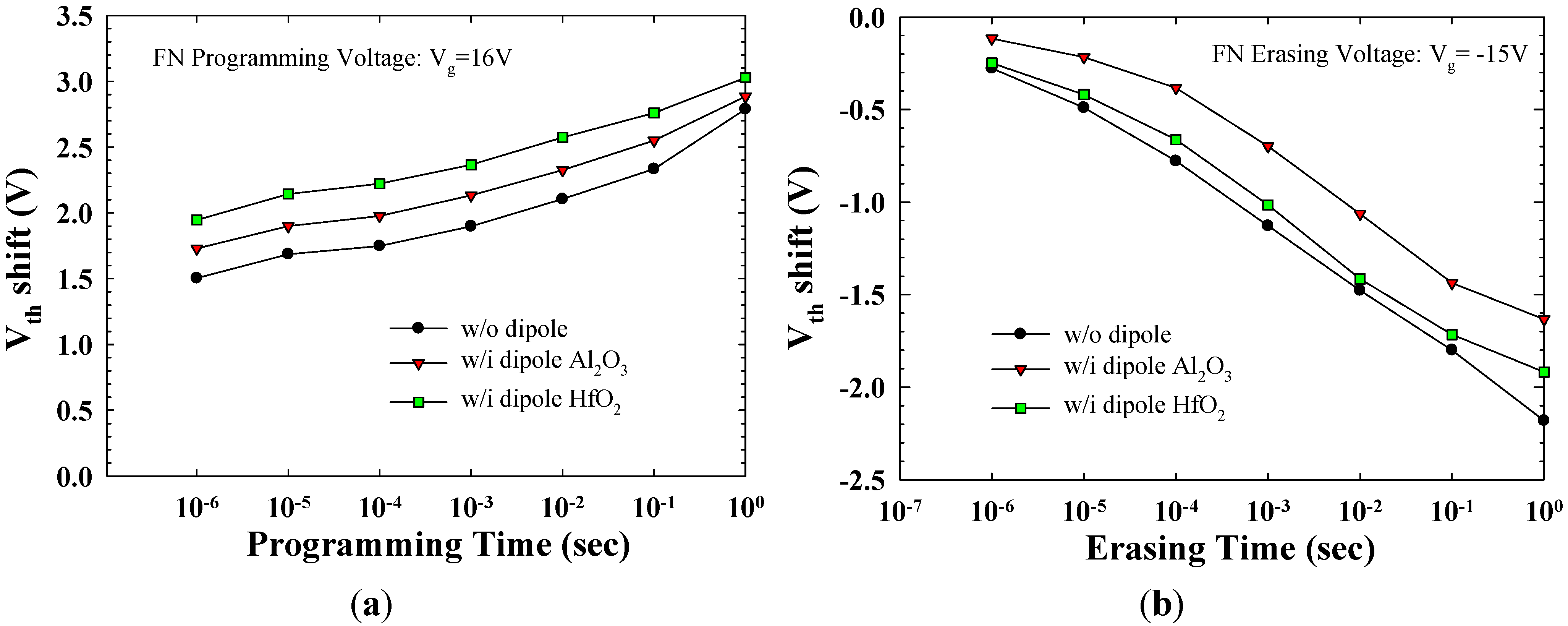
| Dipole engineering | w/o Dipole | w/i Dipole Al2O3 | w/i Dipole HfO2 |
|---|---|---|---|
| Tunneling oxide | SiO2 40 Å | SiO2 40 Å | SiO2 40 Å |
| Dipole layer | – | Al2O3 10 Å | HfO2 10 Å |
| Trapping layer | HfSiOx 100 Å | HfSiOx 100 Å | HfSiOx 100 Å |
| Blocking oxide | Al2O3 100 Å | Al2O3 100 Å | Al2O3 100 Å |
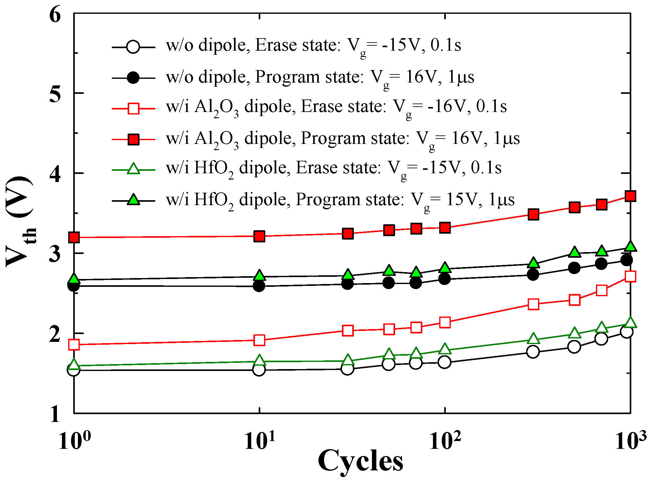
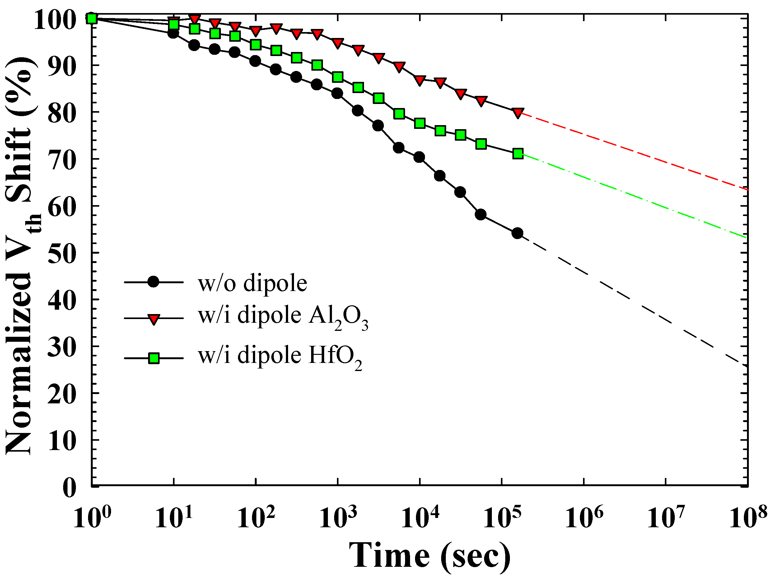
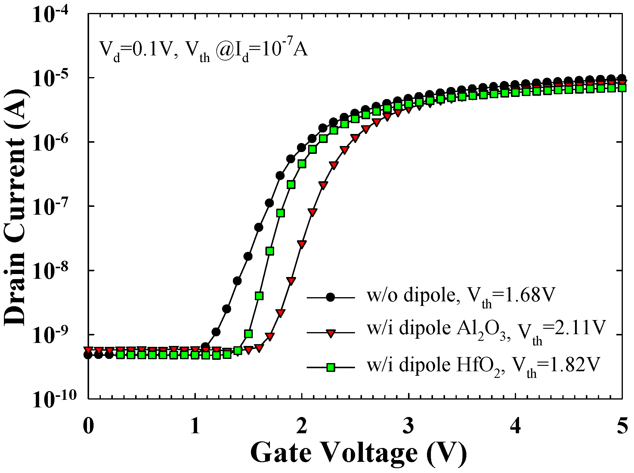
3. Results and Discussion


4. Conclusions
Acknowledgments
Author Contributions
Conflicts of Interest
References
- Li, Y.; Quader, K.N. NAND Flash Memory: Challenges and Opportunities. Computer 2013, 46, 23–29. [Google Scholar] [CrossRef]
- Lin, Y.H.; Chien, C.H. Nanoscale 2-bit/cell HfO2 Nanocrystal Flash Memory. IEEE Trans. Nanotechnol. 2012, 11, 412–417. [Google Scholar] [CrossRef]
- Wu, C.C.; Yang, W.L.; Chang, Y.M.; Liu, S.H.; Hsiao, Y.P. Plasma-Enhanced Storage Capability of SONOS Flash Memory. Int. J. Electrochem. Sci. 2013, 8, 6678–6685. [Google Scholar]
- Hung, M.F.; Wu, Y.C.; Tang, Z.Y. High Performance Gate-All-Around Poly-Si Nanowire with Si Nanocrystals Nonvolatile Memory. Appl. Phys. Lett. 2011, 98, 162108. [Google Scholar] [CrossRef]
- Chen, L.C.; Wu, Y.C.; Lin, T.C.; Huang, J.Y.; Hung, M.F.; Chen, J.H.; Chang, C.Y. Poly-Si Nanowire Nonvolatile Memory with Nanocrystal Indium-Gallium-Zinc-Oxide Charge-Trapping Layer. IEEE Electron. Device Lett. 2010, 31, 1407–1409. [Google Scholar] [CrossRef]
- Lin, Y.H.; Chien, C.H. HfO2 Nanocrystal Memory on SiGe Channel. Solid State Electron. 2013, 80, 5–9. [Google Scholar] [CrossRef]
- Zhao, C.; Zhao, C.Z.; Taylor, S.; Chalker, P.R. Review on Non-Volatile Memory with High-k Dielectrics: Flash for Generation Beyond 32 nm. Materials 2014, 7, 5117–5145. [Google Scholar] [CrossRef]
- Lin, Y.H.; Wu, Y.C.; Hung, M.F.; Chen, J.H. Charge Storage Characteristics of Pi-Gate Poly-Si Nanowires TaN-Al2O3-Si3N4-SiO2-Si Flash Memory. Int. J. Electrochem. Sci. 2012, 7, 8648. [Google Scholar]
- Beug, M.F.; Melde, T.; Czernohorsky, M.; Hoffmann, R.; Paul, J.; Knoefler, R.; Tilke, A.T. Analysis of TANOS memory cells with sealing Oxide Containing Blocking Dielectric. IEEE Trans. Electron Devices 2010, 57, 1590–1596. [Google Scholar] [CrossRef]
- Lee, C.H.; Choi, K.I.; Cho, M.K.; Song, Y.H.; Park, K.C.; Kim, K. A Novel SONOS Structure of SiO2/SiN/Al2O3 with TaN Metal Gate for Multi-Giga Bit Flash Memories. In Proceedings of the IEEE International Electron Devices Meeting, Washington, DC, USA, 8–10 December 2003; pp. 26.5.1–26.5.4.
- Kittl, J.A.; Opsomer, K.; Popovici, M.; Menou, N.; Kaczer, B.; Wang, X.P.; Adelmann, C.; Pawlak, M.A.; Tomida, K.; Rothschild, A.; et al. High-k dielectrics for future generation memory devices. Microelectron. Eng. 2009, 86, 1789–1795. [Google Scholar]
- Chen, F.H.; Pan, T.M.; Chiu, F.C. Metal-Oxide-High-k-Oxide-Silicon Memory Device Using a Ti-Doped Dy2O3 Charge-Trapping Layer and Al2O3 Blocking Layer. IEEE Trans. Electron Devices 2011, 58, 3847–3851. [Google Scholar] [CrossRef]
- Liu, S.H.; Wu, C.C.; Yang, W.L.; Lin, Y.H.; Chao, T.S. Ion-Bombarded and Plasma-Passivated Charge Storage Layer for SONOS-Type Nonvolatile Memory. IEEE Trans. Electron Devices 2014, 61, 3179–3185. [Google Scholar] [CrossRef]
- Breuil, L.; Lisoni, J.G.; Blomme, P.; van den bosch, G.; van Houdt, J. HfO2 Based High-k Inter-Gate Dielectrics for Planar NAND Flash Memory. IEEE Electron Device Lett. 2013, 35, 45–47. [Google Scholar] [CrossRef]
- Pavunny, S.P.; Scott, J.F.; Katiyar, R.S. Lanthanum Gadolinium Oxide: A New Electronic Device Material for CMOS Logic and Memory Devices. Materials 2014, 7, 2669–2696. [Google Scholar] [CrossRef]
- Chiang, T.Y.; Wu, Y.H.; Ma, W.C.Y.; Kuo, P.Y.; Wang, K.T.; Liao, C.C.; Yeh, C.R.; Yang, W.L.; Chao, T.S. Characteristics of SONOS-Type Flash Memory with in Situ Embedded Silicon Nanocrystals. IEEE Trans. Electron Devices 2010, 57, 1895–1902. [Google Scholar] [CrossRef]
- Clark, R.D. Emerging Applications for High K Materials in VLSI Technology. Materials 2014, 7, 2913–2944. [Google Scholar] [CrossRef]
- The International Technology Roadmap for Semiconductors (ITRS). Available online: http://www.itrs.net/ (accessed on 8 April 2014).
- Collaert, N.; Demand, M.; Ferain, I.; Lisoni, J.; Singanamallan, R.; Zimmerman, P.; Yim, Y.S.; Schram, T.; Mannaert, G.; Goodwin, M.; et al. Tall Triple-Gate Devices with TiN/HfO2 Gate Stack. In Proceedings of the Symposia on VLSI Technology and Circuits, Kyoto, Japan, 14–16 June 2005; pp. 108–109.
- Singanamalla, R.; Yu, H.Y.; Daele, B.V.; Kubicek, S.; Meyer, K.D. Effective Work-Function Modulation by Aluminum-Ion Implantation for Metal-Gate Technology (Poly-Si/TiN/SiO2). IEEE Electron Device Lett. 2007, 28, 1089–1091. [Google Scholar] [CrossRef]
- Weber, O.; Andrieu, F.; Mazurier, J.; Casse, M.; Garros, X.; Leroux, C.; Martin, F.; Perreau, P.; Fenouillet-Beranger, C.; Barnola, S.; et al. Work-Function Engineering in Gate First Technology for Multi-VT Dual-Gate FDSOI CMOS on UTBOX. In Proceedings of the IEEE International Electron Devices Meeting, San Francisco, CA, USA, 6–8 December 2010; pp. 3.4.1–3.4.4.
- Chau, R. Advanced Metal Gate/High-k Dielectric Stacks for High Performance CMOS Transistors. In Proceedings of the AVS 5th International Microelectronics Interfaces Conference, Santa Clara, CA, USA, 1–4 February 2004; pp. 3–5.
- Chau, R. Application of High-k Gate Dielectrics and Metal Gate Electrodes to Enable Silicon and Non-Silicon Logic Nanotechnology. Microelectron. Eng. 2005, 80, 1–6. [Google Scholar] [CrossRef]
- Huang, A.P.; Zheng, X.H.; Xiao, Z.S.; Wang, M.; Di, Z.F.; Chu, P.K. Interface Dipole Engineering in Metal Gate/High-k Stacks. Chin. Sci. Bull. 2012, 57, 2872–2878. [Google Scholar] [CrossRef]
- Sivasubramani, P.; Kim, J.; Kim, M.J.; Gnade, B.E.; Wallace, R.M. Effect of Composition on the Thermal Stability of Sputter Deposited Hafnium Aluminate and NitridedHafnium Aluminate Dielectrics on Si (100). Jpn. J. Appl. Phys. 2007, 101, 114108. [Google Scholar] [CrossRef]
- Lerouxa, C.; Baudota, S.; Charbonniera, M.; van der Geesta, A.; Caubetb, P.; Toffolia, A.; Blaisea, P.; Ghibaudoc, G.; Martina, F.; Reimbolda, G. Investigating Doping Effects on High-k Metal Gate Stack for Effective Work Function Engineering. Solid State Electron 2013, 88, 21–26. [Google Scholar] [CrossRef]
- Kita, K.; Toriumi, A. Intrinsic Origin of Electric Dipoles Formed at High-k/SiO2 Interface. Appl. Phys. Lett. 2009, 94, 132902. [Google Scholar] [CrossRef]
- Sivasubramani, P.; Böscke, T.S.; Huang, J.; Young, C.D.; Kirsch, P.D.; Krishnan, S.A.; Quevedo-Lopez, M.A.; Govindarajan, S.; Ju, B.S.; Harris, H.R.; et al. Dipole Moment Model Explaining nFETVt Tuning Utilizing La, Sc, Er, and Sr Doped HfSiON Dielectrics. In Proceedings of the Symposia on VLSI Technology and Circuits, Kyoto, Japan, 12–16 June 2007; pp. 68–69.
- He, G.; Liu, M.; Zhu, L.Q.; Chang, M.; Fang, Q.; Zhang, L.D. Effect of Postdeposition Annealing on the Thermal Stability and Structural Characteristics of Sputtered HfO2 Films on Si (1 0 0). Surf. Sci. 2005, 576, 67–75. [Google Scholar] [CrossRef]
- Yu, H.Y.; Li, M.F.; Cho, B.J.; Yeo, C.C.; Joo, M.S.; Kwong, D.L.; Pan, J.S.; Ang, C.H.; Zheng, J.Z.; Ramanathan, S. Energy Gap and Band Alignment for (HfO2)x (Al2O3)1−x on (100) Si. Appl. Phys. Lett. 2002, 81, 376–378. [Google Scholar] [CrossRef]
- Xu, K.; Sio, H.; Kirillov, O.A.; Dong, L.; Xu, M.; Ye, P.D.; Gundlach, D.; Nguyen, N.V. Band Offset Determination of Atomic-Layer-Deposited Al2O3 and HfO2 on InP by Internal Photoemission and Spectroscopic Ellipsometry. Jpn. J. Appl. Phys. 2007, 113, 024504. [Google Scholar] [CrossRef]
© 2015 by the authors; licensee MDPI, Basel, Switzerland. This article is an open access article distributed under the terms and conditions of the Creative Commons Attribution license (http://creativecommons.org/licenses/by/4.0/).
Share and Cite
Lin, Y.-H.; Yang, Y.-Y. Work Function Adjustment by Using Dipole Engineering for TaN-Al2O3-Si3N4-HfSiOx-Silicon Nonvolatile Memory. Materials 2015, 8, 5112-5120. https://doi.org/10.3390/ma8085112
Lin Y-H, Yang Y-Y. Work Function Adjustment by Using Dipole Engineering for TaN-Al2O3-Si3N4-HfSiOx-Silicon Nonvolatile Memory. Materials. 2015; 8(8):5112-5120. https://doi.org/10.3390/ma8085112
Chicago/Turabian StyleLin, Yu-Hsien, and Yi-Yun Yang. 2015. "Work Function Adjustment by Using Dipole Engineering for TaN-Al2O3-Si3N4-HfSiOx-Silicon Nonvolatile Memory" Materials 8, no. 8: 5112-5120. https://doi.org/10.3390/ma8085112
APA StyleLin, Y.-H., & Yang, Y.-Y. (2015). Work Function Adjustment by Using Dipole Engineering for TaN-Al2O3-Si3N4-HfSiOx-Silicon Nonvolatile Memory. Materials, 8(8), 5112-5120. https://doi.org/10.3390/ma8085112