Article

Preparation and Characterization of Surface Photocatalytic Activity with NiO/TiO2 Nanocomposite Structure

1
Institute of Electro-Optical and Materials Science, National Formosa University, Huwei, Yunlin 63201, Taiwan
2
Industrial Technology Research Institute South, Liujia Shiang, Tainan 734, Taiwan
*
Author to whom correspondence should be addressed.
Materials 2015, 8(7), 4273-4286; https://doi.org/10.3390/ma8074273
Submission received: 24 May 2015 / Revised: 26 June 2015 / Accepted: 3 July 2015 / Published: 13 July 2015
(This article belongs to the Special Issue Selected Papers from ICETI2014)

Abstract

:
This study achieved a nanocomposite structure of nickel oxide (NiO)/titanium dioxide (TiO2) heterojunction on a TiO2 film surface. The photocatalytic activity of this structure evaluated by decomposing methylene blue (MB) solution was strongly correlated to the conductive behavior of the NiO film. A p-type NiO film of high concentration in contact with the native n-type TiO2 film, which resulted in a strong inner electrical field to effectively separate the photogenerated electron-hole pairs, exhibited a much better photocatalytic activity than the controlled TiO2 film. In addition, the photocatalytic activity of the NiO/TiO2 nanocomposite structure was enhanced as the thickness of the p-NiO film decreased, which was beneficial for the migration of the photogenerated carriers to the structural surface.

1. Introduction

In recent decades, the photocatalytic degradation of organic and inorganic pollutants using oxide semiconductor-based materials had been extensively studied [1,2,3,4,5]. Among these materials, titanium dioxide (TiO2) has been the most popular candidate due to its chemical stability, optical transparency at visible wavelength, high refractive index, non-toxic nature, and low cost [6,7,8]. Engineers have demonstrated that the TiO2 material with the anatase structure has the best photocatalytic activity [9,10]. However, as the photocatalytic activity of the crystalline TiO2 with anatase structure is constrained by the absorption edge at the UV wavelength, the recombination of the photo-generated electron-hole pairs, and the specific surface area, researchers have sought to modify the surface property of the TiO2 material by introducing metallic or non-metallic elements as well as enriching its reaction area. For instance, incorporating nitrogen and carbon elements into TiO2 films produces efficient ions, resulting in the light absorption shift of the film to the visible-light region [11,12], whereas the elements Fe, Ag, Pt, and F are commonly used as doping atoms in the TiO2 film to inhibit the recombination of the carriers under light irradiation [13,14,15,16]. In addition, the photocatalytic activity of TiO2 film was effectively improved with the achievement of a nano-texture on the film’s surface, which was beneficial for increasing the adsorption of all reactants [16,17]. Currently, constructing a heterojunction between TiO2 and semiconductors or oxide materials with appropriate band gap and band position, such as CdS, Cu2O, ZnO, Bi2O3, SrIn2O4, RuO2, and NiO, has offered a promising alternative to effectively enhance the photocatalytic activity of TiO2 [18,19,20,21,22,23,24,25]. For instance, Uddin et al. [23,25] used an impregnation method to introduce a transition-metal oxide of ruthenium oxide (RuO2) which possessed a high work function of about 6.1 eV on the sol-gel processed TiO2 nanopowders. The resulting RuO2/TiO2 mesoporous heterojunction exhibited a significant enhancement in the photocatalytic activity due to the improved separation of photogenetrated electron-hole pairs resulting from the internal electric field. Furthermore, since the TiO2 material is a well-known n-type material, nickel oxide (NiO) which shows a p-type semiconducting nature with a high band gap of about 3.86 eV [26], it is also expected to be a promising candidate on contact to TiO2 since an additive pathway associated with the formation of an inner electrical field between the heterojunction which is favorable for the separation of the photo-generated electrons and holes to different semiconductors in the p-NiO/n-TiO2 heterojunction structure, can be achieved. Although a few groups have had success in preparing a NiO/TiO2 heterojunction and the improvements in the resulting photocatalytic activity as a mechanism of the p-n junction have been discussed briefly [20,27], the photocatalytic activity of the NiO/TiO2 heterojunction structure influenced by the conduction behavior and thickness of the NiO film has been rarely investigated.
In this work, we developed a simple method to achieve the NiO/TiO2 nanocomposite structure on a TiO2 film surface via a rapid thermal annealing (RTA) process. The photocatalytic activities of the annealed NiO/TiO2 nanocomposite structures correlating with the electrical properties and crystalline structures of the NiO films, were evaluated and discussed. Evidence of the separation of the photo-generated electron-hole pairs achieved from these NiO/TiO2 nanocomposite structures was determined from the on-off process of the photocurrent response. In addition, the thickness of the NiO film in the NiO/TiO2 nanocomposite structure was varied in order to understand the resulting photocatalytic activity influenced by the diffusion of the photogenerated carriers in the NiO film to the structural surface.

2. Material Preparation and Experimental Procedure

Hydro-oxygenated amorphous titanium dioxide (TiO2) films with a thickness of 200 nm were deposited onto silicon and quartz substrates after a 20 nm-thick nickel seed layered evaporation and a sequential oxidation at 550 °C for 1 min under oxygen ambient, using plasma enhanced chemical vapor deposition (PECVD) at a temperature of 200 °C. A titanium tetra-isopropoxide [Ti(OC3H7)4, TTIP] liquid source was utilized as the titanium precursor through a heated bubbling cylinder at 70 °C, with nitrogen as the carrier gas and intermixed with pure oxygen gas in a mix box. All the gas pipelines were heated to 100 °C to prevent condensation of the precursor and gas mixture. The deposition pressure, rf power, and gas flow rate of the TTIP/O2 gas mixture were controlled at 40 Pa, 100 W, and 120/20 sccm, respectively. To optimize the film’s photocatalytic activity, these amorphous TiO2 films deposited onto the seed layer were then annealed at 600 °C for 30 min under ambient oxygen to result in the film crystallization with the anatase phase (denoted as the controlled TiO2 film hereafter). The reason for the TiO2 film deposited onto the seed layer and the mechanism responsible for the controlled TiO2 film exhibiting a better photocatalytic activity than that of the TiO2 film directly deposited onto the substrate, has been discussed elsewhere [28]. A metallic Ni film with a thickness of 20 nm was then evaporated onto the controlled TiO2 film surface, and sequentially annealed at 450 °C, 550 °C and 650 °C, respectively, under oxygen ambient for 1 min to realize the surface with the NiO/TiO2 nanocomposite structure. Another set of 200 nm-thick Ni films directly deposited onto the silicon substrate were also prepared and treated using the same RTA process to investigate the evolution of the film’s electrical and crystalline properties. In addition, the thickness of the Ni film deposited on the controlled TiO2 film was varied from 10 to 50 nm to further optimize the photocatalytic activity achieved by the NiO/TiO2 nanocomposite structure.
The film thickness of the controlled TiO2 film, the pure NiO films, and the samples with the NiO/TiO2 nanocomposite structure were measured using a surface profile system (Dektak 6M, Veeco, New York, NY, USA). Surface roughness and morphologies were examined using atomic force microscopy (AFM, DI-3100, Veeco, New York, NY, USA) and a field emission scanning electron microscope (FE-SEM, JSM-6700F, JEOL, Tokyo, Japan) operated at 3 kV. The chemical bond states and optical transmittance of the TiO2 films with and without the surface heterojunction structure were examined by Fourier transform infrared (FTIR) spectrometry (FT/IR-4100, JASCO, Halifax, NS, Canada) and a UV-Vis-NIR spectrophotometer (UVD 3500, Labomed, Inc., Los Angeles, CA, USA), respectively. The crystalline structure of these two samples and the pure NiO films annealed at various temperatures as well as the as-deposited Ni film were examined using a grazing incident X-ray diffractometer (GIXRD) at 30 kV and 30 mA using Cu1 radiation (D-500, Siemens, Munich, Germany). The electrical properties of the controlled TiO2 film and the Ni films treated by the RTA process were measured using the van der Pauw Hall measurements (HMS-5000, Ecopia Anyang, Korea) at room temperature. The photocatalytic activity of these TiO2 films with and without the surface heterojunction structure as well as the pure NiO film was evaluated from the decolorization of an aqueous methylene blue (MB) solution (20 mg·L−1 with a pH value approximately of 7.0 ± 0.1) at ambient temperature using a UV light irradiation (λ = 365 nm) at a constant intensity of 1 mW·cm−2. The photo-excited currents for the TiO2 films both with and without the surface NiO/TiO2 heterojunction, irradiated by a Xe lamp, were also conducted by a semiconductor parameter analyzer (HP4156C, Aglient, Santa Clara, CA, USA), followed by patterning the surface of the films with interdigital transducer (IDT) Al electrodes.

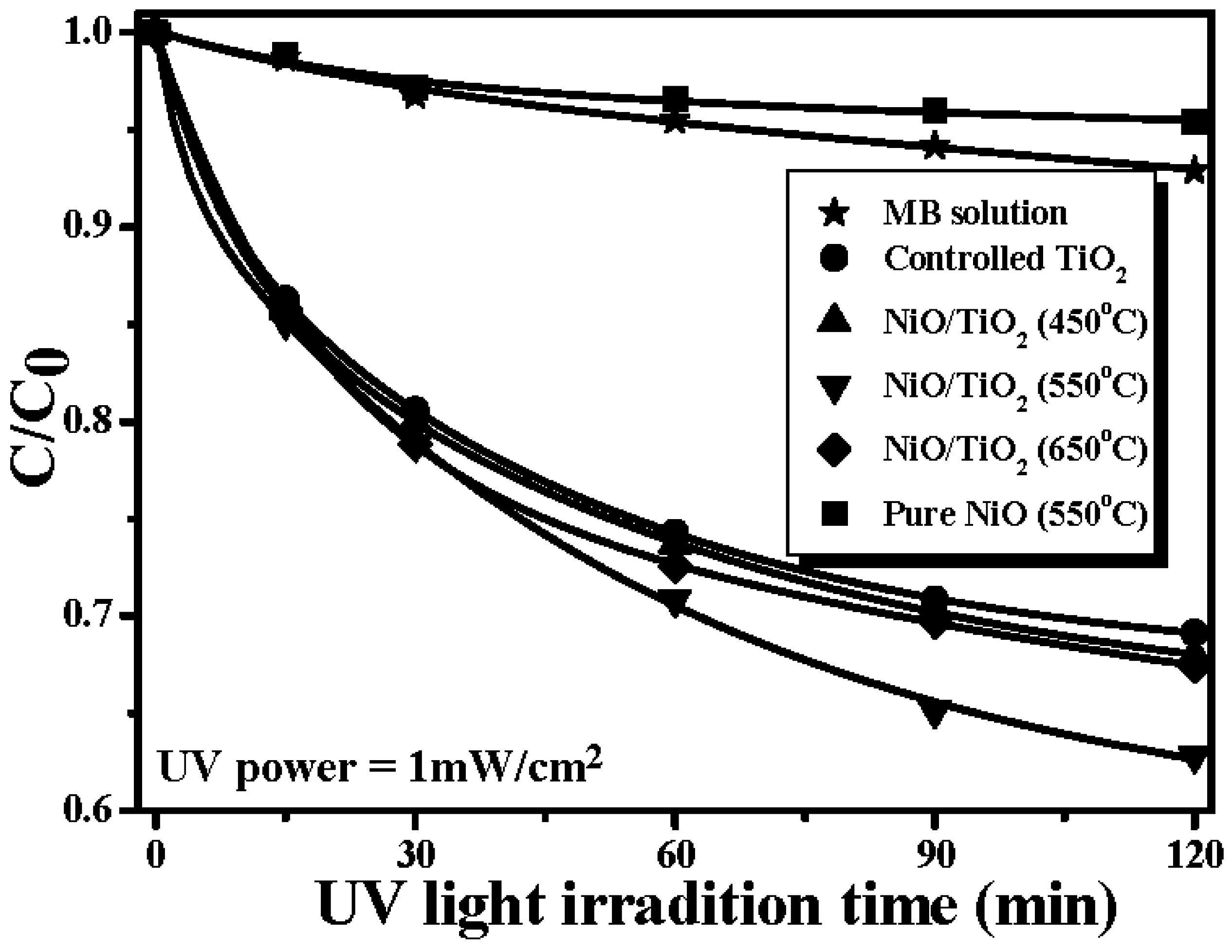
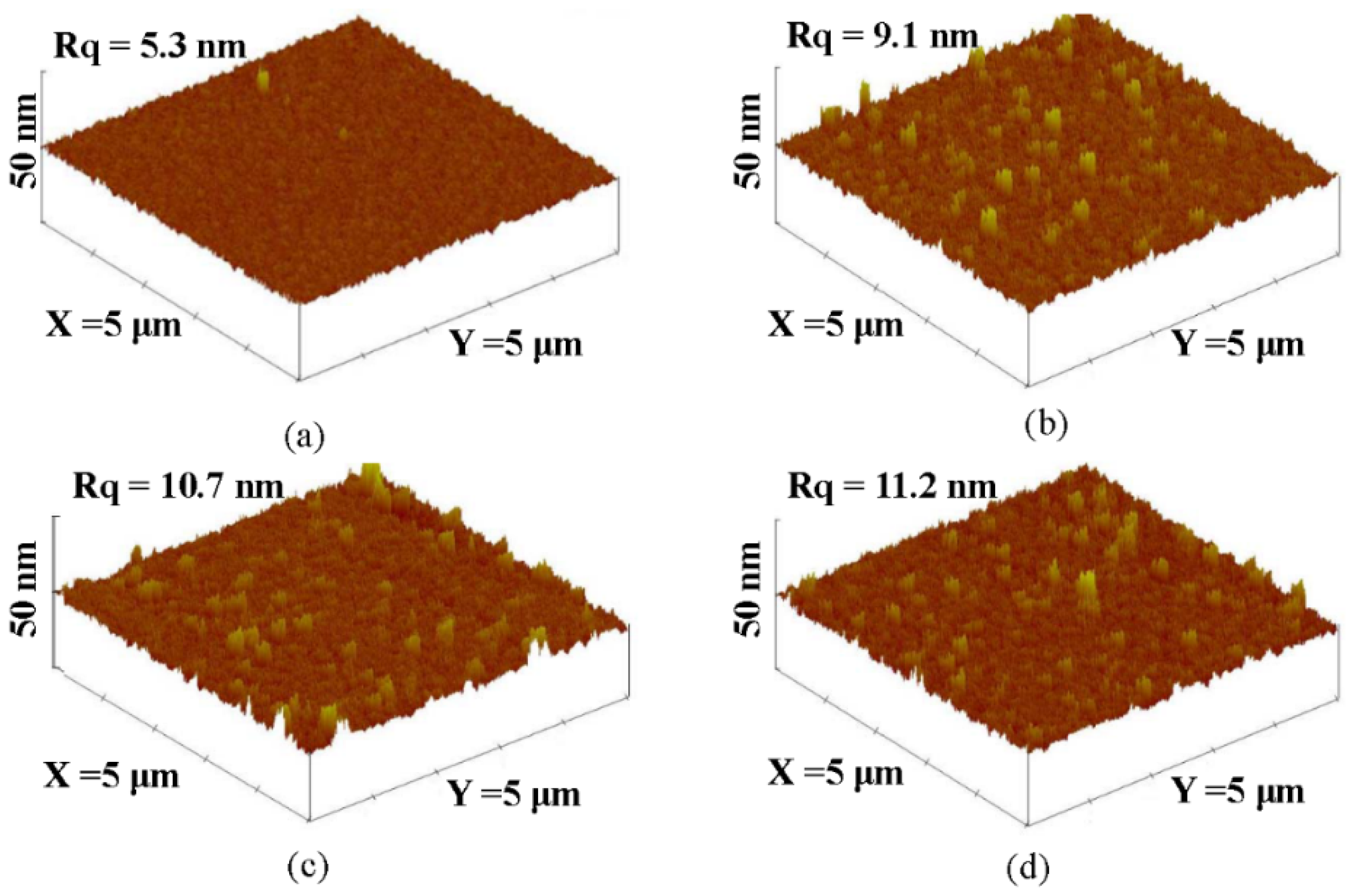
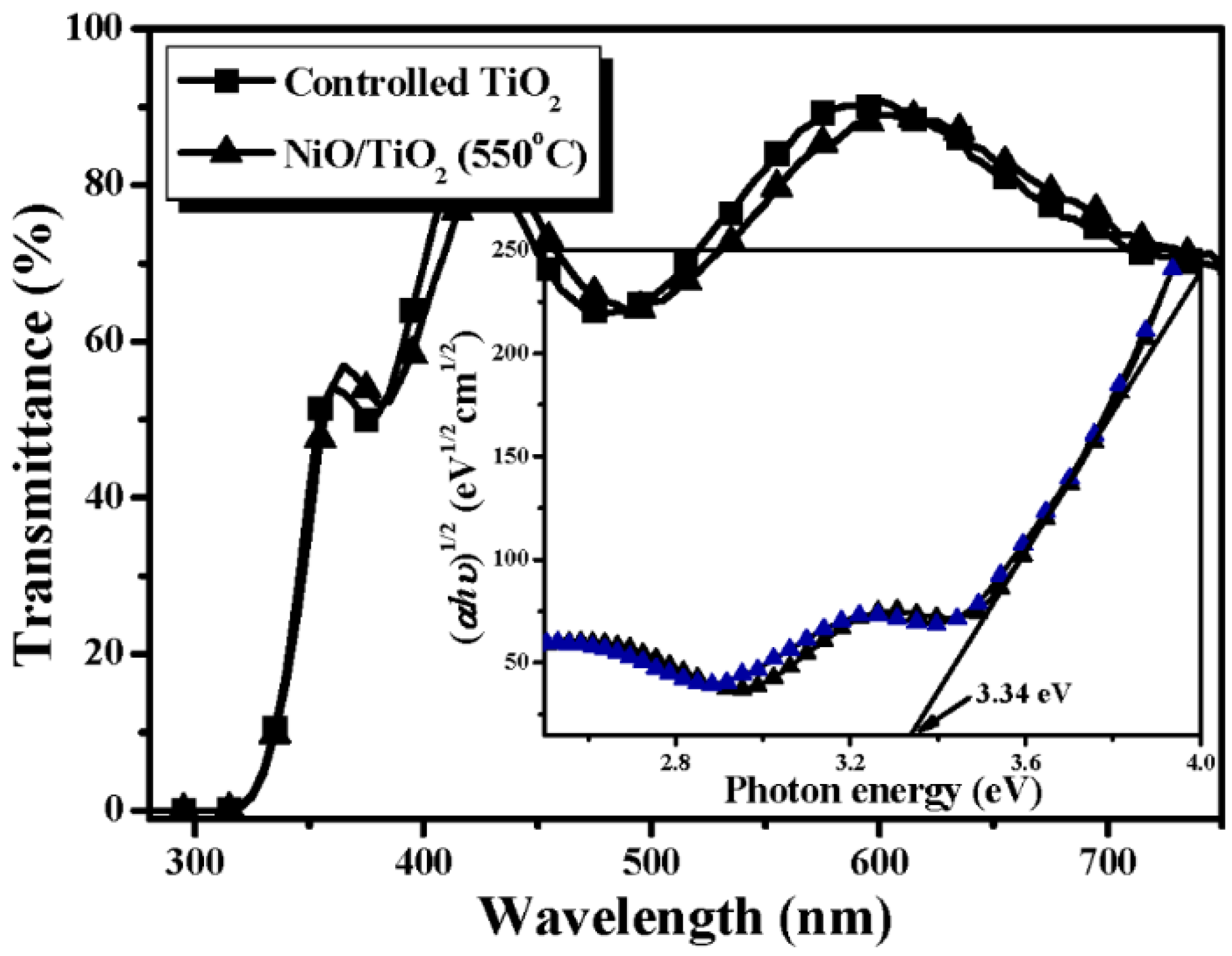
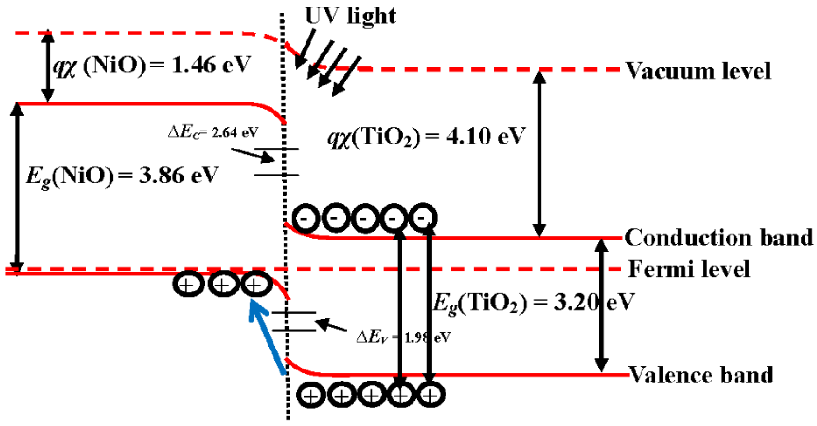
3. Results and Discussion
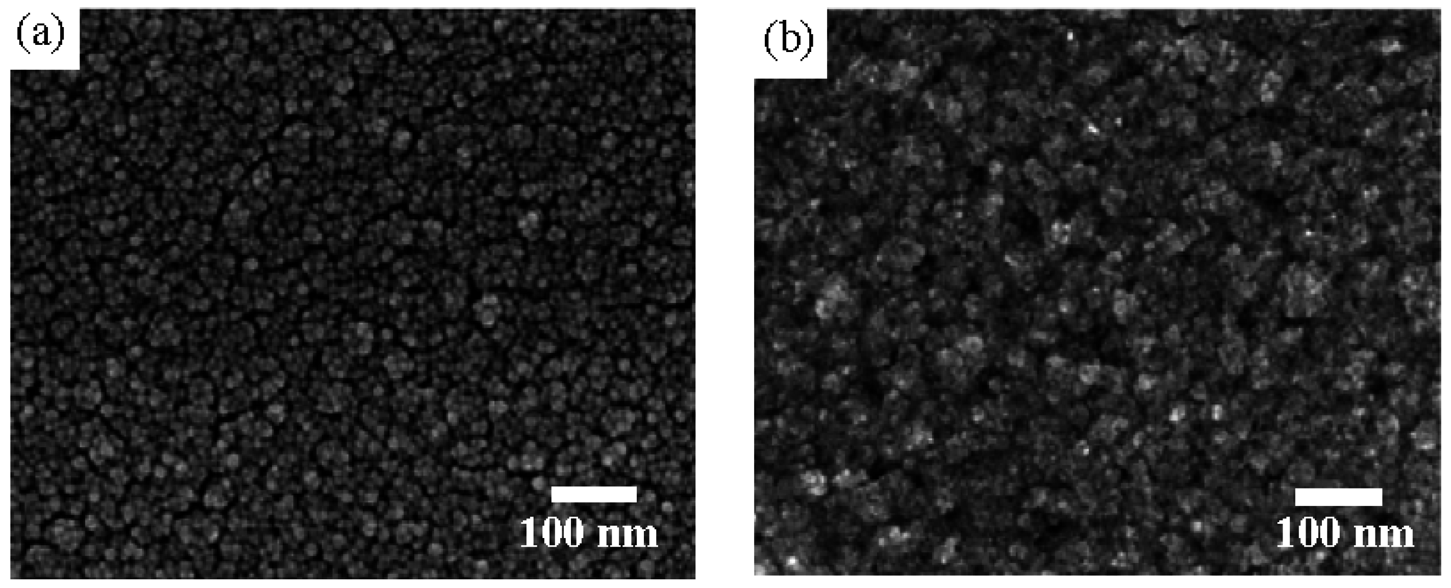
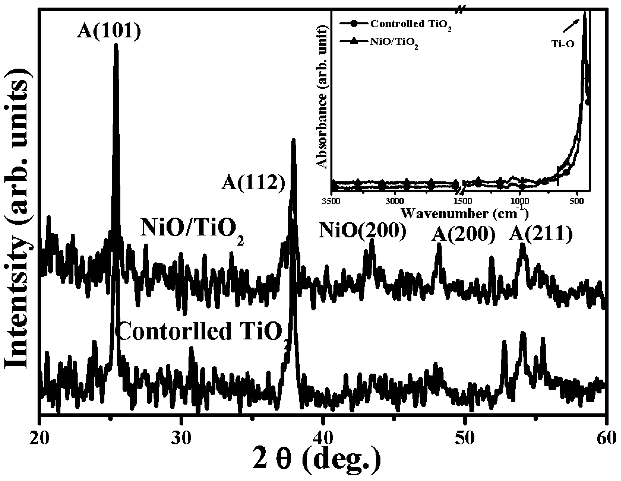
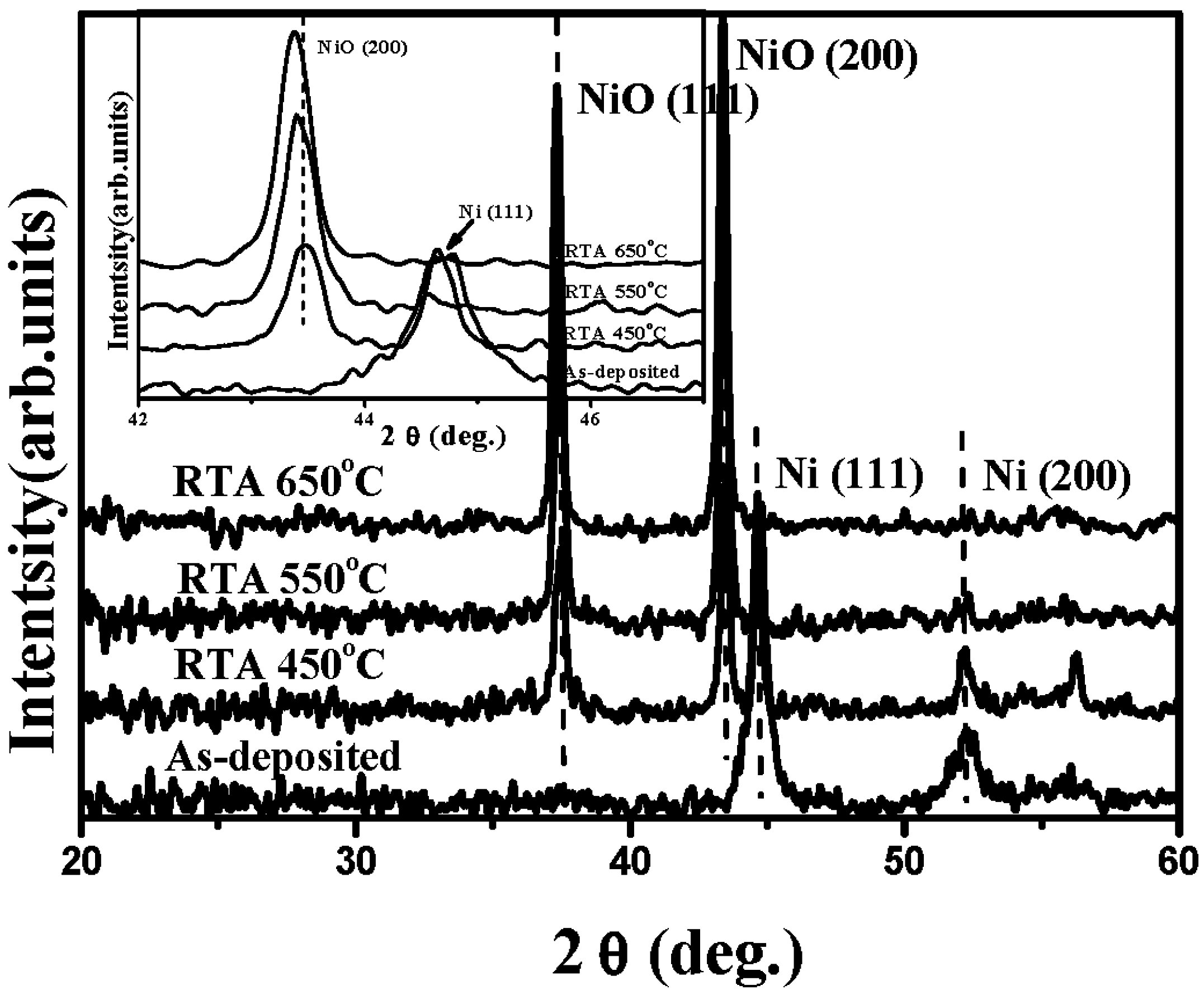
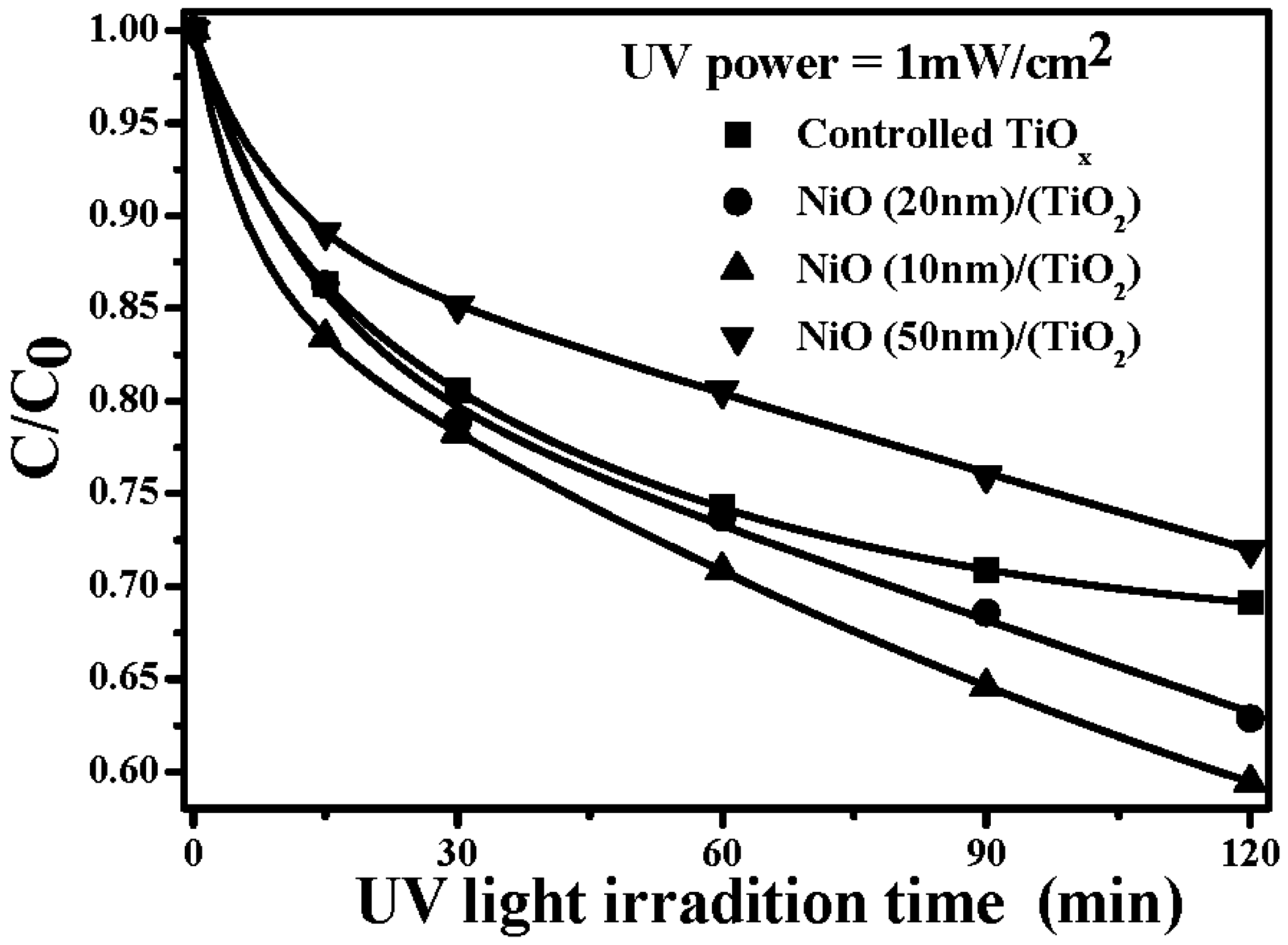
Figure 1 shows the UV light-induced catalyses of the controlled TiO2 film, the NiO/TiO2 nanocomposite structures treated by the RTA process at temperatures of 450 °C, 550 °C, and 650 °C, respectively, and the pure NiO film treated by the RTA process at 550 °C to degrade the MB solution (the degradation of the MB solution directly irradiated by the UV light is provided for comparison). The UV light-induced photodegradation of the MB solution was significantly enhanced by introducing the controlled TiO2 film, while that of the pure NiO film was useless to degrade the MB solution. However, although the pure NiO film surface was inactive to the UV light irradiation, the NiO/TiO2 nanocomposite structure exhibited a faster photodegradation rate to the MB solution compared to that of the controlled TiO2 film. The rate constant, k, which represents the film’s photocatalytic activity, is evaluated from the photodegradation rate of the MB solution using the following equation [29]:
ln ( c c 0 ) = k t
where, C and C0 are the concentration of the MB solution at UV light irradiation time of t = 0 and t, respectively. Table 1 summarizes the rate constant (k) and root-mean-square surface roughness (Rq) of the controlled TiO2 film and the NiO/TiO2 nanocomposite structure treated by the RTA process at temperatures of 450 °C, 550 °C and 650 °C, respectively. Clearly, all these TiO2 films with the surface nanocomposite structure possessed a higher rate constant to photo-degrade the MB solution than that of the controlled TiO2 film (0.0232 min−1). The best photocatalytic activity that corresponded to a rate constant of 0.0304 min−1 was obtainable from the Ni film deposited onto the TiO2 film surface and then rapidly annealed at 550 °C for 1 min under oxygen ambient. The surface roughness of the controlled TiO2 film and the NiO/TiO2 nanocomposite structures annealed at 450 °C, 550 °C and 650 °C, respectively, are illustrated in Figure 2a–d. As shown in Figure 2b–d, many significant protrusions were distributed over the RTA-treated NiO/TiO2 nanocomposite surface, thereby resulting in the obvious increase in the surface roughness. However, despite the fact that the surface roughness of the NiO/TiO2 nanocomposite structure annealed at 450 °C exhibited a high value of 9.1 nm compared to the controlled TiO2 film (~5.3 nm), which might be beneficial for enriching the surface specific area of the TiO2 film, the increase in the rate constant (~0.0236 min−1), as listed in Table 1, was limited compared to the controlled TiO2 film. In contrast to the 450 °C-annealed sample, the NiO/TiO2 nanocomposite structure annealed at 550 °C, which showed a surface roughness of 10.7 nm, possessed the highest rate constant of 0.0304 min−1. Figure 3a,b respectively, show the surface morphologies of the controlled TiO2 film and 550 °C-annealed NiO/TiO2 nanocomposite structures. Many fine grains were distributed over the controlled TiO2 film surface, whereas the grains were not apparent when the TiO2 film surface was coated with the thin NiO layer, and the surface was a feature of significant clusters which could be linked to the protrusions, as observed in Figure 2d. The possible reason for such surface morphology was attributed to the 20 nm-thick Ni layer grown in form of separate islands and then agglomerated by the sequential rapid oxidation process [30,31]. In addition, since the pure NiO film was inactive to the UV light irradiation, the increase in the surface roughness of the NiO/TiO2 nanocomposite structures as evidence of the NiO agglomeration would not have led to the enhancement of the photocatalytic activity. Accordingly, the rough surface measured from these annealed NiO/TiO2 nanocomposite structure was not the dominant mechanism responsible for the improvement in their rate constants, as listed in Table 1. Figure 4 depicts the optical transmittance of the controlled TiO2 film and the NiO/TiO2 nanocomposite structure annealed at 550 °C. It can be seen that both samples showed optical transparency within the visible wavelengths and then sharply decreased at the near UV wavelength. The average transmittance in the visible wavelengths (400–700 nm) of the annealed NiO/TiO2 nanocomposite structure (~77.5%) was only a little lower than that of the controlled TiO2 film (78.2%). In addition, the optical energy bandgap of the annealed NiO/TiO2 nanocomposite structure determined from the (αhν)1/2 versus the photon energy as shown in the inset figure, was identical to that of the controlled TiO2 film (~3.34 eV), indicating that the upper NiO film did not affect the optical absorption of the TiO2 film. The crystalline structures of the controlled TiO2 film and the 550 °C-annealed NiO/TiO2 nanocomposite structure are shown in Figure 5 (the associated FTIR spectra also are given in the inset figure). Though the signal was a little weak due to the total thickness of these films, only about 200 nm, the peaks showed evidence that the crystalline TiO2 still could be identified. The controlled TiO2 film exhibited a polycrystalline structure with only the anatase structure being dominated by the (101) phase determined from JCPDS 21-1272 (the diffraction peaks for the anatase phase are marked as “A”, with the diffraction planes given in parentheses). For the NiO/TiO2 nanocomposite system annealed at a temperature of 550 °C, the diffraction peaks and their positions were identical to those observed from the controlled TiO2 film, except for the appearance of the NiO (200) phase. The crystal size (D) of the two samples derived from the full width at half maximum (FWHM) of the preferred orientation of the A(101) phase adopting the Scherrer formula is expressed below [32]:
D = k λ β cos θ
where k (=0.9) is a constant, λ is the wavelength of the X-ray radiation (~0.154 nm), β is the FWHM in radians, and θ is the Bragg diffraction angle. The anatase crystallite size of the NiO/TiO2 nanocomposite structure estimated from the FWHM of the A(101) was about 27.3 nm, a value slightly smaller than that of the controlled TiO2 film (~28.9 nm). In addition, only one intense and sharp peak located at about 432 cm−1 was observed from both the FTIR spectra of these two samples, which was assigned as the Ti-O chemical bond [33], indicating that the deposition and the sequential RTA process did not result in a change to the crystalline structure or the bond states of the TiO2 film. In order to elucidate the mechanism responsible for the apparent increase in the photocatalytic activity of the NiO/TiO2 nanocomposite structure annealed at 550 °C, a thick Ni film was directly deposited on to the silicon substrate and then treated with the same RTA process. Figure 6 shows the XRD patterns of the as-deposited Ni film and the films annealed at temperatures of 450 °C, 550 °C, and 650 °C, respectively. The XRD pattern of the as-deposited Ni film included a significant peak at approximately 44.8° and a weak peak at 52.2°, which were in turn assigned as the Ni(111) and Ni(200) phase according to JCPDS 45-1027. When the Ni film was treated by the RTA process at a temperature of 450 °C, the diffraction peaks located at about 37.7° and 43.3°, which were classified as NiO(111) and NiO(200) according to JCPDS 47-1049, became the dominant signals in the XRD pattern, indicating crystalline evolution from the metallic Ni to the oxidized NiO structure. For the RTA temperatures of 550 °C and 650 °C, only two intense and sharp diffraction peaks identified as the NiO(111) and NiO(200) phases were obtained in their XRD patterns as evidence of the complete oxidation of the Ni film and the growth of the NiO crystallite structure. In addition, the shift of the NiO(200) diffraction peak toward a lower 2θ angle for the samples annealed at 550 °C and 650 °C shown in the inset figure was demonstrated as lattice expansion induced by interstitial oxygen atoms, which is consistent with previous research [34]. The electrical properties of the as-deposited Ni film, the films annealed at temperatures of 450 °C, 550 °C and 650 °C, respectively, and the controlled TiO2 film are listed in Table 2. The as-deposited Ni film performed its metallic nature with very high electron carriers of 8.23 × 1023 cm−3 and an ultra low resistivity (1.64 × 10⁻⁶ Ω·cm). However, as the metallic Ni and oxidized NiO structure coexisted in the sample annealed at a temperature of 450 °C, as shown in Figure 6, such phase separation resulted in the film’s resistivity being too large (higher than 105 Ω·cm) to be measured. Notably, a high hole carrier of 2.60 × 1018 cm−3 was obtained from the metallic Ni completely transformed to the NiO structure as the film annealed at a temperature of 550 °C. The activation of the interstitial oxygen atoms that were classified as acceptors in the annealed NiO film, was one possible reason for the conversion of the conduction from n-type to p-type behavior. Moreover, as an elevated annealing temperature on the film was also prone to cause outdiffusion of the atoms from the film surface, especially for the oxygen atoms, which acted as donor defects (i.e., oxygen vacancies) [35], the hole concentration of the NiO film annealed at 650 °C was thus apparently decreased to 1.29 × 1014 cm−3 as a consequence of the compensation of the hole carriers. These NiO films, which showed p-type conduction in contact with the controlled TiO2 film, that performed n-type with a concentration of 3.55 × 1013 cm−3, as listed in Table 2, thus achieved the surface p-n heterojunction structure.
Figure 1. UV light-induced catalyses of the controlled TiO2 film, the NiO/TiO2 nanocomposite structures treated by the RTA (rapid thermal annealing) process at temperatures of 450 °C, 550 °C, and 650 °C, respectively, and the pure NiO film treated by the RTA process at 550 °C to degrade the MB (methylene blue) solution (the degradation of the MB solution directly irradiated by the UV light is provided for comparison).
Materials 08 04273 g001
Table 1. Rate constant (k) and root-mean-square surface roughness (Rq) of the controlled TiO2 film and the NiO/TiO2 nanocomposite structure treated by the RTA process at temperatures of 450 °C, 550 °C, and 650 °C, respectively.
ValuesControlled TiO2NiO/TiO2 (450 °C)NiO/TiO2 (550 °C)NiO/TiO2 (650 °C)
k (min−1)0.02320.02360.03040.0251
Rq (nm)5.39.110.711.2
Table 2. Electrical properties of the as-deposited Ni film, the controlled TiO2 film, and the films annealed at temperatures of 450 °C, 550 °C and 650 °C, respectively.
SamplesConcentration (cm−3)Mobility (cm2·V−1·s−1)Resistivity (Ω·cm)
As-deposited Ni-8.23 × 10234.741.64 × 10−6
NiO (450 °C)N/AN/AN/A
NiO (550 °C)2.60 × 101821.61.11 × 10−1
NiO (650 °C)1.29 × 10144.301.13 × 104
Controlled TiO2-3.55 × 101340.84.32 × 103
Figure 2. Surface roughness of the (a) controlled TiO2 film; and the NiO/TiO2 nanocomposite structures with an additive RTA process at temperature of (b) 450 °C; (c) 550 °C; (d) 650 °C, respectively.
Materials 08 04273 g002
Figure 3. Surface morphologies of the (a) controlled TiO2 film and (b) the NiO/TiO2 nanocomposite structures annealed at 550 °C.
Materials 08 04273 g003
Figure 4. Optical transmittance of the controlled TiO2 film and the NiO/TiO2 nanocomposite structure annealed at 550 °C (the associated optical energy bandgaps also are derived from the inset figure).
Materials 08 04273 g004
Figure 5. XRD patterns of the controlled TiO2 film and the 550 °C-annealed NiO/TiO2 nanocomposite structure (the associated FTIR spectra also are given in the inset figure).
Materials 08 04273 g005
A schematic energy band diagram of the 550 °C annealed p-NiO/n-TiO2 heterojunction structure adopting Anderson’s rule is plotted in Figure 7. The bandgaps, Eg, of NiO and TiO2, which have been taken from the reported works, are 3.86 and 3.20 eV, respectively, while the electron affinities, , for these two materials are 1.46 and 4.10 eV, respectively [36,37,38,39]. As can be seen in this figure, the band offset for holes (1.98 eV) is a little smaller than that for electrons (2.64 eV). In addition, a space charge region originating from the p-n junction led to an inner electrical field in the NiO/TiO2 interface. Thus, the photo-generated electron-hole pairs in the TiO2 film surface under UV light irradiation would be effectively separated with the effect of the built-in voltage formed by the p-NiO/n-TiO2 heterojunction. The photon-generated holes in the TiO2 film surface could easily flow into the NiO film, whereas the photo-generated electrons were blocked by the significant barrier and restrained in the TiO2 film surface. The life time of these photo-generated carriers in the p-NiO/n-TiO2 nanocomposite structure was thus expected to be prolonged as a consequence of the inhibition of their recombination. Accordingly, an apparent increase in the rate constant evaluated from the decomposition to the MB solution, as listed in Table 1, was obtainable from the NiO/TiO2 nanocomposite structure with an RTA treatment at a temperature of 550 °C. The UV light-induced catalysts for the MB solution using the 550 °C-annealed p-NiO/n-TiO2 nanocomposite structures, with the thickness of the NiO film being 10, 20 and 50 nm, respectively, are illustrated in Figure 8. It is worth noting that, although the p-NiO/n-TiO2 heterojunction structure was demonstrated to be beneficial for separating the photo-generated electron-hole pairs, the thickness of the NiO film also strongly affected the resulting photocatalytic activity of the MB solution. The photodegradation rate of the MB solution was further increased for the NiO/TiO2 nanocomposite structure with a NiO film thickness of 10 nm (k ~ 0.0327 min−1), whereas the 50 nm-thick NiO film in contact with the TiO2 film surface, resulted in an apparent reduction in the rate constant (0.0144 min−1), as evaluated from the photo-induced decomposition to the MB solution. This revealed that a thin NiO film that corresponded to a short diffusion path for the photo-induced holes which migrated to the structural surface to react with the MB molecules was also crucial for affecting the resulting photocatalytic activity. Figure 9 shows the transient photo-excited current responses of the controlled TiO2 film and the 550 °C-annealed NiO/TiO2 nanocomposite structure. The photo-induced catalysts of both samples were reliable as evidence of the repeatable photocurrent responses. The dark current of the NiO/TiO2 nanocomposite structure (~2.2 × 10⁻⁸ A) was only a little higher than that of the controlled TiO2 film (~1.9 × 10⁻⁸ A) under the same irradiation power, whereas its photo-induced current (~2.3 × 10⁻⁵ A) was an order of magnitude higher than that of the controlled TiO2 film (~2.2 × 10⁻⁶ A), revealing the increase in the quantum efficiency accomplished by this p-n heterojunction structure. The recombination time of the photo-generated electro-hole pairs evaluated from the on-off process was also prolonged from 4 min to 7 min as the 10 nm-thick Ni film was deposited onto the controlled TiO2 film and rapidly oxidized at 550 °C for 1 min under oxygen ambient.
Figure 6. XRD patterns of the as-deposited Ni film and the films annealed at temperatures of 450 °C, 550 °C, and 650 °C, respectively (the inset figure shows a high resolution of the NiO(200) and Ni(111) planes).
Materials 08 04273 g006
Figure 7. A schematic energy band diagram of the 550 °C annealed p-NiO/n-TiO2 heterojunction structure.
Materials 08 04273 g007
Figure 8. UV light-induced catalysts of the MB solution using the 550 °C-annealed p-NiO/n-TiO2 nanocomposite structures, with the thickness of the NiO film being 10, 20 and 50 nm, respectively.
Materials 08 04273 g008
Figure 9. Transient photo-excited current responses of the controlled TiO2 film (curve A) and the 550 °C-annealed NiO/TiO2 nanocomposite structure (curve B).
Materials 08 04273 g009

4. Conclusions

Thin Ni metal was deposited onto TiO2 film and rapidly oxidized at 450 °C, 550 °C and 650 °C, respectively, for 1 min under oxygen ambient to result in a surface with the NiO/TiO2 nanocomposite structure. Although the RTA process on the NiO/TiO2 nanocomposite structure did not result in a change to the crystalline structure and optical absorption of the TiO2 film and the surface NiO film were also inactive in response to UV light irradiation, these samples possessed a higher rate constant than that of the controlled TiO2 film, as evaluated from the films decomposing the MB solution. According to the investigations of the crystalline structure and the electrical properties of the single NiO films, the evolution of the photocatalytic activities of these annealed NiO/TiO2 nanocomposite structures were strongly correlated to the conduction type and carrier concentration of the NiO films. The 450 °C-annealed NiO/TiO2 nanocomposite structure, of which the NiO film showed insulated behavior due to the phase separations of Ni and NiO, possessed a rate constant (0.0236 min−1) only slightly higher than that of the controlled TiO2 film (0.0232 min−1). By contrast, the rate constant of the 550 °C-annealed NiO/TiO2 nanocomposite structure, in which the NiO film behaved as p-type conduction with a high carrier concentration of 2.60 × 1018 cm−3, was apparently increased to 0.0304 min−1. In addition, the rate constant was again decreased to 0.0251 min−1 for the sample annealed at 650 °C while the NiO film had a low hole concentration of 1.29 × 1014 cm−3. The reason responsible for the improvement in the photocatalytic activity was the formation of the surface p-n heterojunction achieved from the annealed NiO/TiO2 nanocomposite structure. The inner electrical field that appeared at the p-NiO/n-TiO2 interface was favorable for the separation of the photo-generated electron-hole pairs in the TiO2 film surface, thereby improving the quantum efficiency as demonstrated from the increase in the photocurrent. The recombination of the photo-generated carriers determined from the on-off time of the photocurrent was also apparently prolonged to 7 min compared to that of the controlled TiO2 film. In addition, by reducing the thickness of the NiO film to 10 nm, the photocatalytic activity of the resulting NiO/TiO2 nanocomposite structure was further enhanced with a rate constant of 0.0327 min−1 as a consequence of the photo-induced carriers, which could migrate to the structural surface more efficiently.

Acknowledgments

This work was supported by Ministry of Science and Technology under MOST 103-2221-E-150-067 and ITRI South under FY 104-AE2.

Author Contributions

Day-Shan Liu organized and designed the experiment procedures; Tai-Hong Chen and Li-Wen Lai wrote the paper; Pei-Yu Li and Hua-Wen Liu executed the film deposition; Jian-Zhi Chen and Yi-You Hong performed the thin film measurements and analysis. All authors read and approved the final version of the manuscript to be submitted.

Conflicts of Interest

The authors declare that there is no conflict of interests regarding the publication of this paper.

References

  1. Lee, K.M.; Abd Hamid, S.B. Simple response surface methodology: Investigation on advance photocatalytic oxidation of 4-chlorophenoxyacetic acid using UV-active ZnO photocatalyst. Materials 2015, 8, 339–354. [Google Scholar] [CrossRef]
  2. Kumar, R.G.; Umar, A. Zinc oxide nanomaterials for photocatalytic degradation of methyl orange: A review. Nanosci. Nanotechnol. Lett. 2014, 6, 631–650. [Google Scholar] [CrossRef]
  3. Kmetyko, A.; Mogyorosi, K.; Gerse, V.; Konya, Z.; Pusztai, P.; Dombi, A.; Hernadi, K. Photocatalytic H2 production using Pt-TiO2 in the presence of oxalic acid: Influence of the noble metal size and the carrier gas flow rate. Materials 2014, 7, 7022–7038. [Google Scholar] [CrossRef]
  4. Bayal, N.; Jeevanandam, P. Sol-gel synthesis of SnO2-MgO nanoparticles and their photocatalytic activity towards methylene blue degradation. Mater. Res. Bull. 2013, 48, 3790–3799. [Google Scholar] [CrossRef]
  5. Uddin, M.T.; Nicolas, Y.; Olvier, C.; Servant, L.; Toupance, T.; Li, S.; Klein, A.; Jaegermann, W. Improved photocatalytic activity in RuO2-ZnO nanoparticulate heterostructures due to inhomogeneous space charge effects. Phys. Chem. Chem. Phys. 2015, 17, 5090–5102. [Google Scholar] [CrossRef] [PubMed]
  6. Liu, D.S.; Lin, T.W.; Huang, B.W.; Juang, F.S.; Lei, P.H.; Hu, C.Z. Light-extraction enhancement in GaN-based light-emitting diodes using grade-refractive-index amorphous titanium oxide films with porous structures. Appl. Phys. Lett. 2009, 94, 143502. [Google Scholar] [CrossRef]
  7. Necula, B.S.; Fratila-Apachitei, L.E.; Zaat, S.A.J.; Apachitei, I.; Duszczyk, J. In vitro antibacterial activity of porous TiO2-Ag composite layers against methicillin-resistant Staphylococcus aureus. Acta Biomater. 2009, 5, 3573–3580. [Google Scholar] [CrossRef] [PubMed]
  8. Fang, Y.L.; Wang, X.M.; Ai, X.L.; Huang, J.G.; Wang, Q.; Wu, T. Sputtered TiOx thin film as compact layer for solid-state dye sensitized solar cells. Ceram. Int. 2014, 40, 15941–15949. [Google Scholar] [CrossRef]
  9. Wang, Y.; Zhang, L.; Deng, K.; Chen, X.; Zou, Z. Low Temperature Synthesis and Photocatalytic Activity of Rutile TiO2 Nanorod Superstructures. J. Phys. Chem. C 2007, 111, 2709–2714. [Google Scholar] [CrossRef]
  10. Wu, C.Y.; Chiang, B.S.; Chang, S.; Liu, D.S. Determination of photocatalytic activity in amorphous and crystalline titanium oxide films prepared using plasma-enhanced chemical vapor deposition. Appl. Surf. Sci. 2011, 257, 1893–1897. [Google Scholar] [CrossRef]
  11. Wu, Z.B.; Dong, F.; Zhao, W.R.; Wang, H.Q.; Liu, Y.; Guan, B.H. The fabrication and characterization of novel carbon doped TiO2 nanotubes, nanowires and nanorods with high visible light photocatalytic activity. Nanotechnology 2009, 20, 235701. [Google Scholar] [CrossRef] [PubMed]
  12. Wang, Y.; Feng, C.X.; Zhang, M.; Yang, J.J.; Zhang, Z.J. Enhanced visible light photocatalytic activity of N-doped TiO2 in relation to single-electron-trapped oxygen vacancy and doped-nitrogen. Appl. Catal. B Environ. 2010, 100, 84–90. [Google Scholar] [CrossRef]
  13. Lin, X.X.; Rong, F.; Ji, X.; Fu, D.G. Visible light photocatalytic activity and Photoelectrochemical property of Fe-doped TiO2 hollow spheres by sol-gel method. J. Sol-Gel Sci. Technol. 2011, 59, 283–289. [Google Scholar] [CrossRef]
  14. Ma, C.; Dong, W.; Fang, L.; Zheng, F.G.; Shen, M.R.; Wang, Z.L. Synthesis of TiO2/Pt/TiO2 multilayer films via radio frequency magnetron sputtering and their enhanced photocatalytic activity. Thin Solid Films 2012, 520, 5727–5732. [Google Scholar] [CrossRef]
  15. Sun, T.; Liu, E.Z.; Fan, J.; Hu, X.Y.; Wu, F.; Hou, W.Q.; Yang, Y.H.; Kang, L.M. High photocatalytic activity of hydrogen production from water over Fe doped and Ag deposited anatase TiO2 catalyst synthesized by solvothermal method. Chem. Engineer. J. 2013, 228, 896–906. [Google Scholar] [CrossRef]
  16. Shih, P.C.; Huang, C.H.; Chen, T.H.; Lai, L.W.; Lu, Y.S.; Liu, D.S. Enhancement on photocatalytic activity of an amorphous titanium oxide film with nano-textured surface by selective-fluorination etching process. Mater. Res. Bull. 2014, 52, 177–182. [Google Scholar] [CrossRef]
  17. Van Overschelde, O.; Guisbiers, G.; Hamadi, F.; Hemberg, A.; Snyders, R.; Wautelet, M. Alternative to classic annealing treatments for fractally patterned TiO2 thin films. J. Appl. Phys. 2008, 104, 103106. [Google Scholar] [CrossRef]
  18. Yang, S.G.; Quan, X.; Li, X.Y.; Liu, Y.Z.; Chen, S.; Chen, G.H. Preparation, characterization and photoelectrocatalytic properties of nanocrystalline Fe2O3/TiO2, ZnO/TiO2, and Fe2O3/ZnO/TiO2 composite film electrodes towards pentachlorophenol degradation. Phys. Chem. Chem. Phys. 2004, 6, 659–664. [Google Scholar]
  19. Zhang, J.; Zhu, H.; Zheng, S.; Pan, F.; Wang, T. TiO2 film/Cu2O microgrid heterojunction with photocatalytic activity under solar light irradiation. Appl. Mater. Inter. 2009, 1, 2111–2114. [Google Scholar] [CrossRef] [PubMed]
  20. Ren, L.; Zeng, Y.P.; Jiang, D. The improved photocatalytic properties of p-type NiO loaded porous TiO2 sheets prepared via freeze tape-casting. Solid State Sci. 2010, 12, 138–143. [Google Scholar] [CrossRef]
  21. Wang, L.; Zhang, J.; Li, C.; Wang, W.; Wang, T. Synthesis, characterization and photocatalytic activity of TiO2 film/Bi2O3 microgrid heterojunction. J. Mater. Sci. Technol. 2011, 27, 59–63. [Google Scholar] [CrossRef]
  22. Yang, G.; Yang, B.; Xiao, T.; Yan, Z. One-step solvothermal synthesis of hierarchically porous nanostructured CdS/TiO2 heterojunction with higher visible light photocatalytic activity. Appl. Surf. Sci. 2013, 283, 402–410. [Google Scholar] [CrossRef]
  23. Uddin, Md.T.; Nicolas, Y.; Olivier, C.; Toupance, T.; Müller, M.M.; Kleebe, H.J.; Rachut, K.; Ziegler, J.; Klein, A.; Jaegermann, W. Preparation of RuO2/TiO2 mesoporous heterostructures and rationalization of their enhanced photocatalytic properties by band alignment investigations. J. Phys. Chem. C 2013, 117, 22098–22110. [Google Scholar] [CrossRef]
  24. Kokane, S.B.; Sartale, S.D.; Betty, C.A.; Sasikala, R. Pd-TiO2-SrIn2O4 heterojunction photocatalyst: Enhanced photocatalytic activity for hydrogen. RSC Adv. 2014, 4, 55539–55547. [Google Scholar] [CrossRef]
  25. Uddin, Md.T.; Babot, O.; Thomas, L.; Oliver, C.; Redaelli, M.; D’Arienzo, M.; Morazzoni, F.; Jaegermann, W.; Rockstroh, N.; Junge, H.; Toupance, T. New insights into the photocatalytic properties of RuO2/TiO2 mesoporous heterostructures for hydrogen production and organic pollutant photodecomposition. J. Phys. Chem. C 2015, 119, 7006–7015. [Google Scholar] [CrossRef]
  26. Ai, L.; Fang, G.; Yuan, L.; Liu, N.; Wang, M.; Li, C.; Zhang, Q.; Li, J.; Zhao, X. Influence of substrate temperature on electrical and optical properties of p-type semitransparent conductive nickel oxide thin films deposited by radio frequency sputtering. Appl. Surf. Sci. 2008, 254, 2401–2405. [Google Scholar] [CrossRef]
  27. Chen, C.J.; Liao, C.H.; Hsu, K.C.; Wu, Y.T.; Wu, C.S. P-N junction mechanism on improved NiO/TiO2 photocatalyst. Catal. Commun. 2011, 12, 1307–1310. [Google Scholar] [CrossRef]
  28. Wu, C.Y.; Hong, S.C.; Hwang, F.T.; Lai, L.W.; Lin, T.W.; Liu, D.S. Effect of nickel oxide seed layers on annealed-amorphous titanium oxide thin films prepared using plasma-enhanced chemical vapor deposition. Thin Solid Films 2011, 520, 320–327. [Google Scholar] [CrossRef]
  29. Li, H.; Zhao, G.; Han, G.; Song, B. Hydrophilicity and photocatalysis of Ti1−xVxO2 films prepared by sol-gel method. Surf. Coat. Technol. 2007, 201, 7615–7618. [Google Scholar] [CrossRef]
  30. Vlachos, D.; Kamaratos, M.; Foulias, S.D.; Argirusis, C.; Borchardt, G. Adsorption of oxygen on a nickel covered SrTiO3(100) surface studied by means of Auger electron spectroscopy and work function measurements. J. Phys. Condens. Mater. 2005, 17, 635–642. [Google Scholar] [CrossRef]
  31. Gayán, P.; Dueso, C.; Abad, A.; Adanez, J.; de Diego, L.F.; Garćia-Labiano, F. NiO/Al2O3 oxygen carriers for chemical-looping combustion prepared by impregnation and deposition-precipitation methods. Fuel 2009, 88, 1016–1023. [Google Scholar] [CrossRef] [Green Version]
  32. Chen, X.; Wang, X.; Hou, Y.; Huang, J.; Wu, L.; Fu, X. The effect of postnitridation annealing on the surface property and photocatalytic performance of N-doped TiO2 under visible light irradiation. J. Catal. 2008, 255, 59–67. [Google Scholar] [CrossRef]
  33. Que, W.; Sun, Z.; Zhou, Y.; Lam, Y.L.; Chan, Y.C.; Kam, C.H. Optical and mechanical properties of TiO2/SiO2/organically modified silane composite films prepared by sol-gel processing. Thin Solid Films 2000, 359, 177–183. [Google Scholar] [CrossRef]
  34. Yang, J.L.; Lai, Y.S.; Chen, J.S. Effect of heat treatment on the properties of non-stoichiometric p-type nickel oxide films deposited by reactive sputtering. Thin Solid Films 2005, 488, 242–246. [Google Scholar] [CrossRef]
  35. Sasi, B.; Gopchandran, K.G. Nanostructured mesoporous nickel oxide thin films. Nanotechology 2007, 18, 115613. [Google Scholar] [CrossRef]
  36. Kroeze, J.E.; Savenije, T.J. The application of a low-bandgap conjugated oligomer for the sensitization of SnO2 and TiO2. Thin Solid Films 2004, 451, 54–59. [Google Scholar] [CrossRef]
  37. Lany, S.; Osorio-Guillen, J.; Zunger, A. Origins of the doping asymmetry in oxides: Hole doping in NiO versus electron doping in ZnO. Phys. Rev. B 2007, 75, 241203. [Google Scholar] [CrossRef]
  38. Lin, Y.H.; Wu, Y.C.; Lai, B.Y. Collection Efficiency enhancement of injected electrons in dye-sensitized solar cells with a Ti interfacial layer and TiCl4 treatment. Int. J. Electrochem. Sci. 2012, 7, 9478–9487. [Google Scholar]
  39. Abbasi, M.A.; Ibupoto, Z.H.; Hussain, M.; Nur, O.; Wilander, M. The fabrication of white light-emitting diodes using the n-ZnO/NiO/p-GaN heterojunction with enhanced luminescence. Nanoscale Res. Lett. 2013, 8, 320. [Google Scholar] [CrossRef] [PubMed]

