
Design on Power Factor Correction of a Digital Soft Switching Single-Phase Arc Welding Power Source

Abstract
:1. Introduction
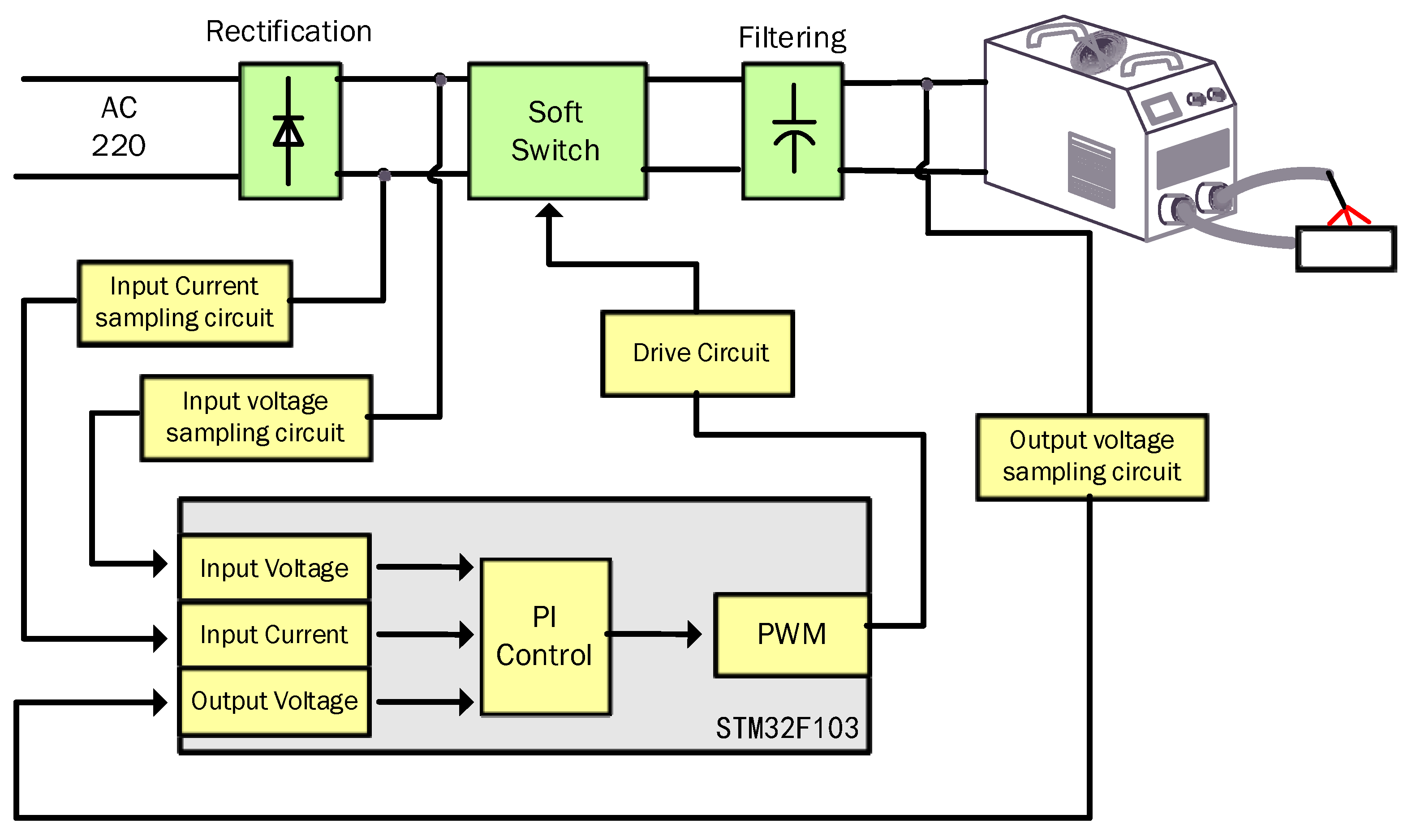
2. Overall Hardware Structure of the System
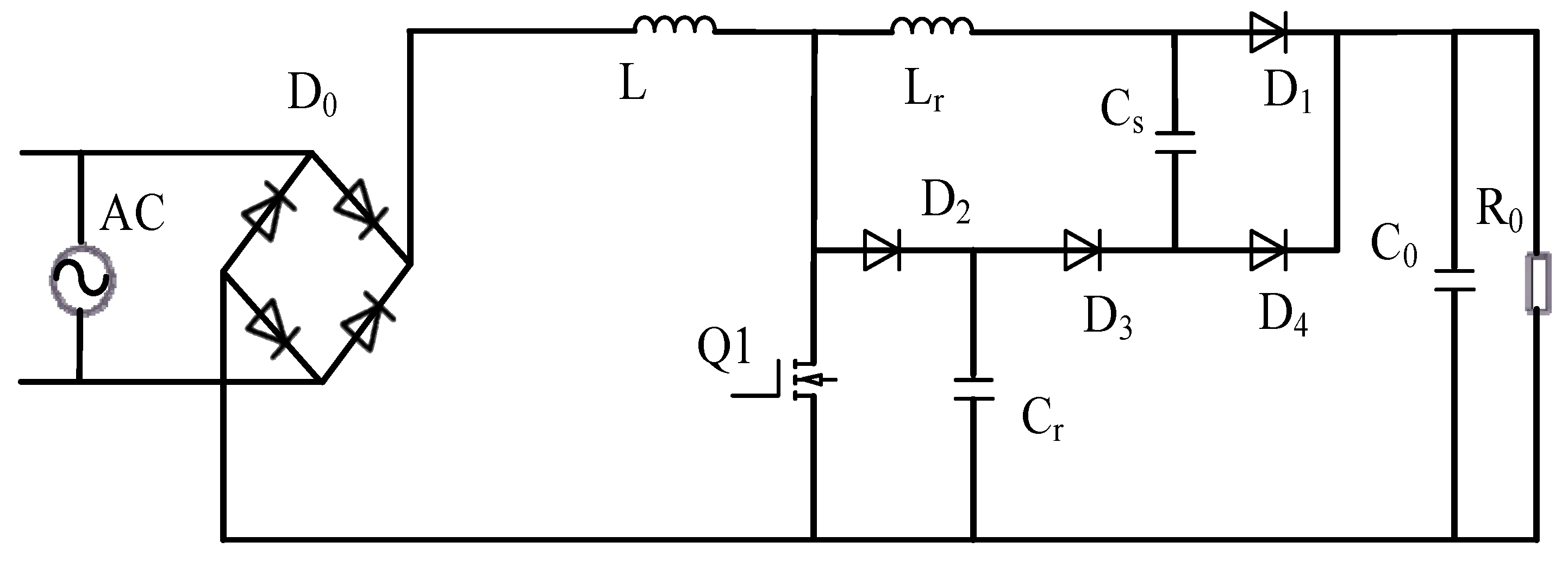
3. Soft Switch Topology and Operating Principle
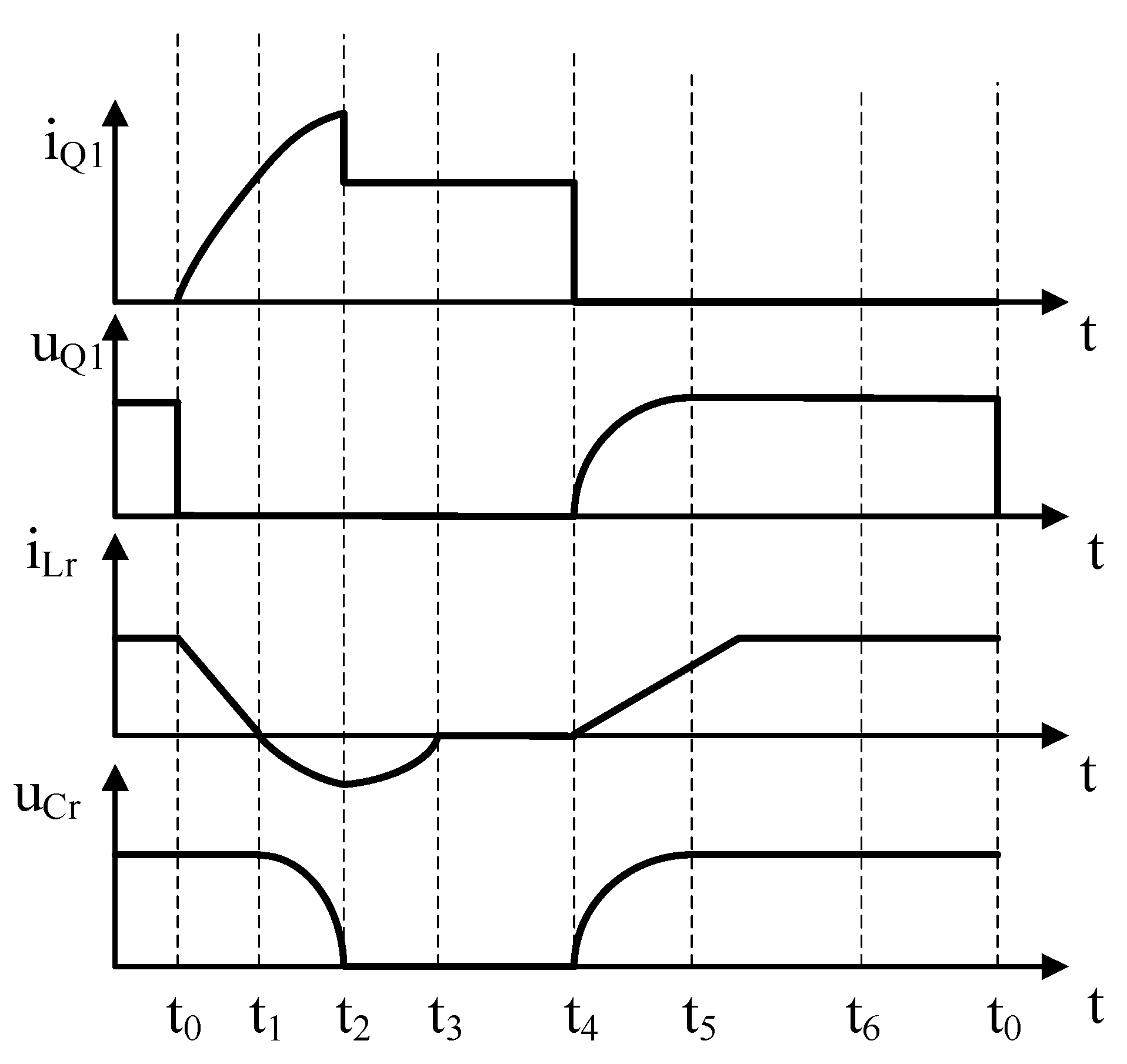
- (1)
- Operating state 1: t < t0
- (2)
- Operating state 2: t0 ≤ t < t1
- (3)
- Operating state 3: t1 ≤ t < t2
- (4)
- Operating state 4: t2 ≤ t < t3
- (5)
- Operating state 5: t3 ≤ t < t4
- (6)
- Operating state 6: t4 ≤ t < t5
- (7)
- Operating state 7: t5 ≤ t < t6
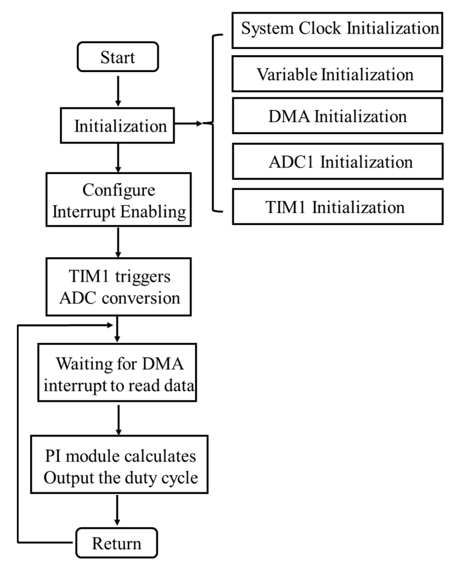
4. Software Design
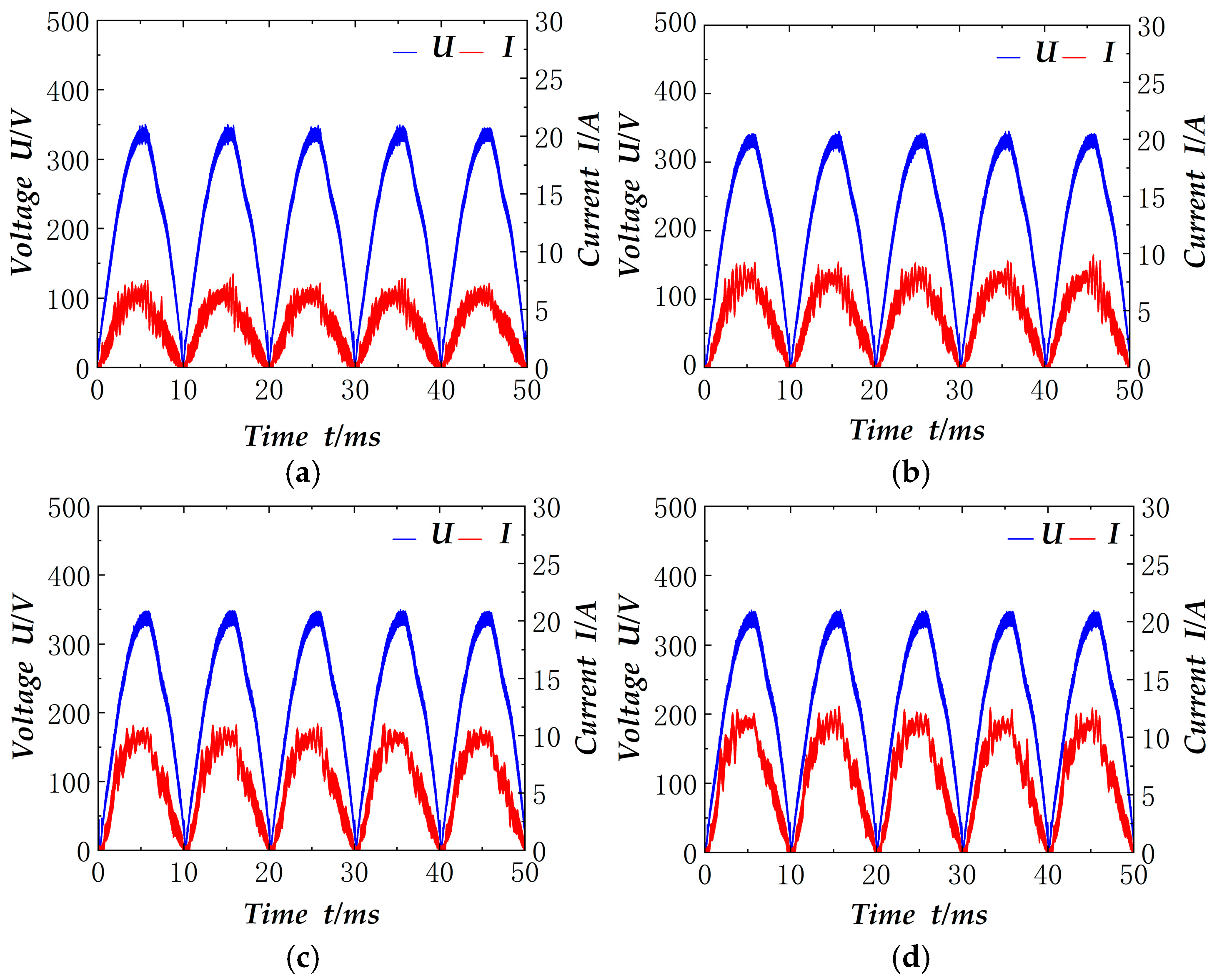
5. Results
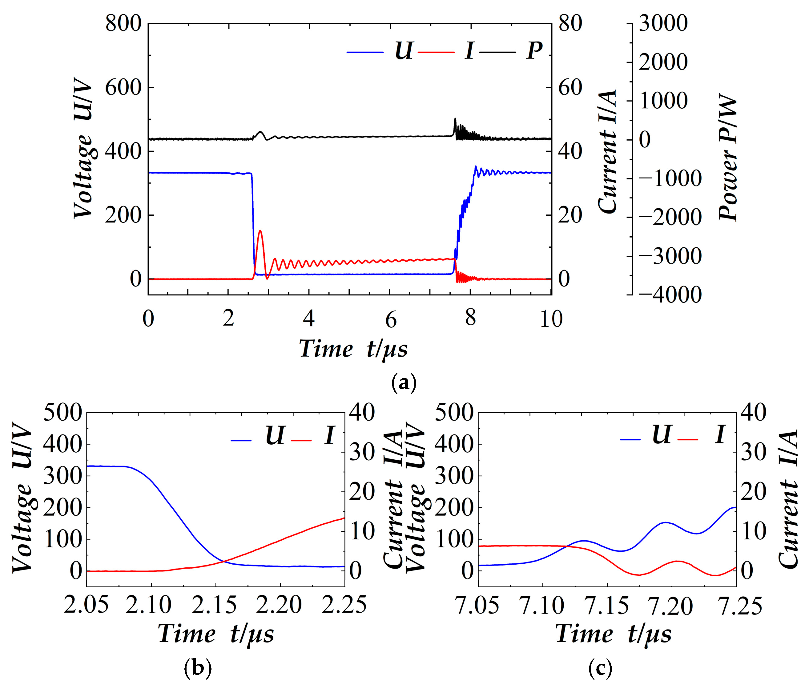
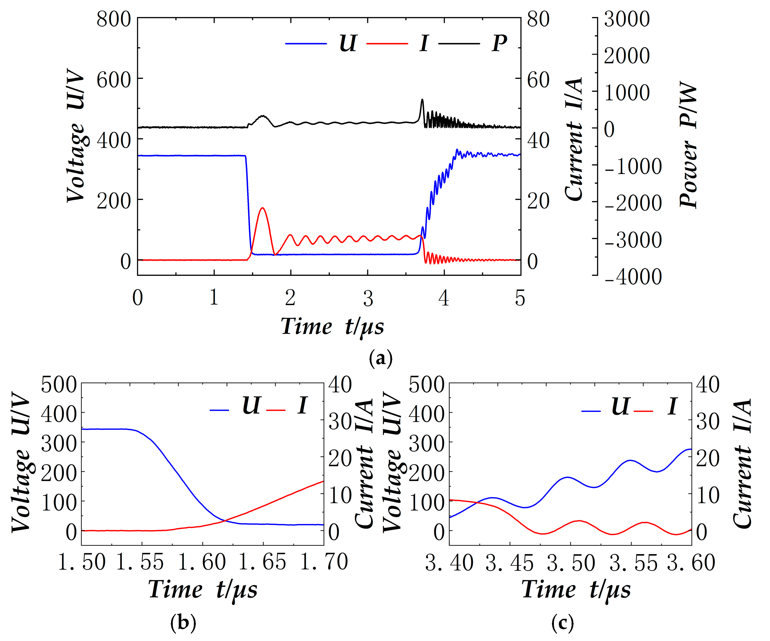
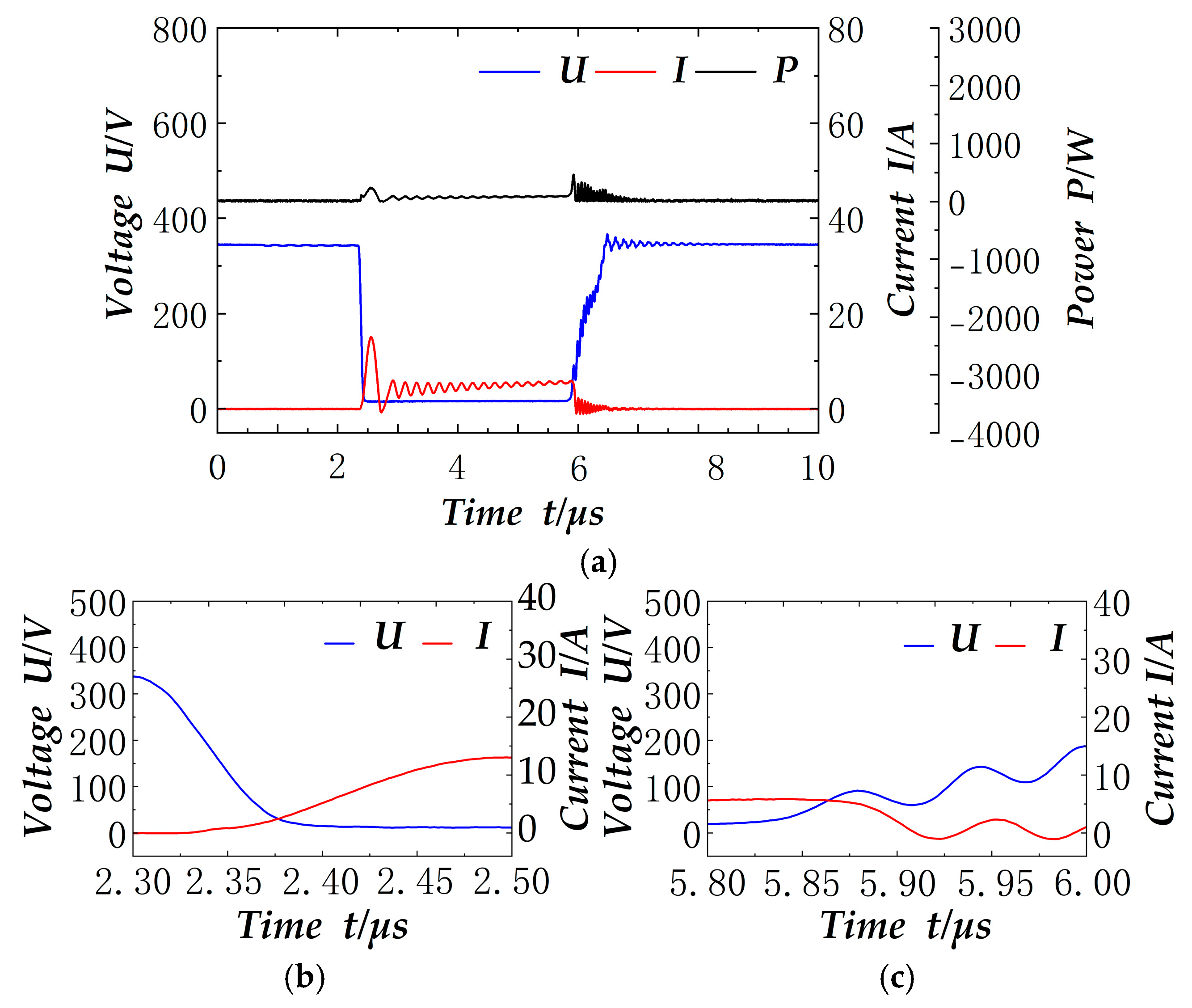
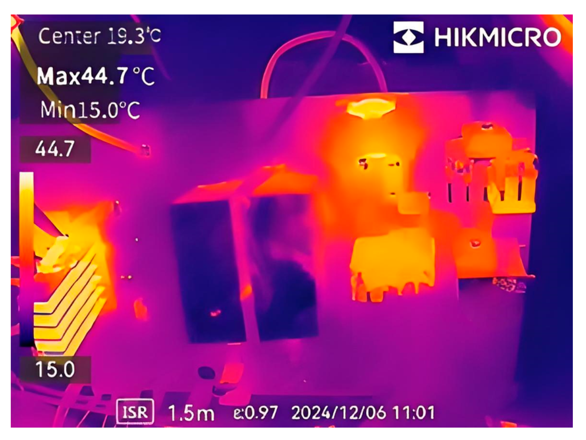
5.1. Soft Switch
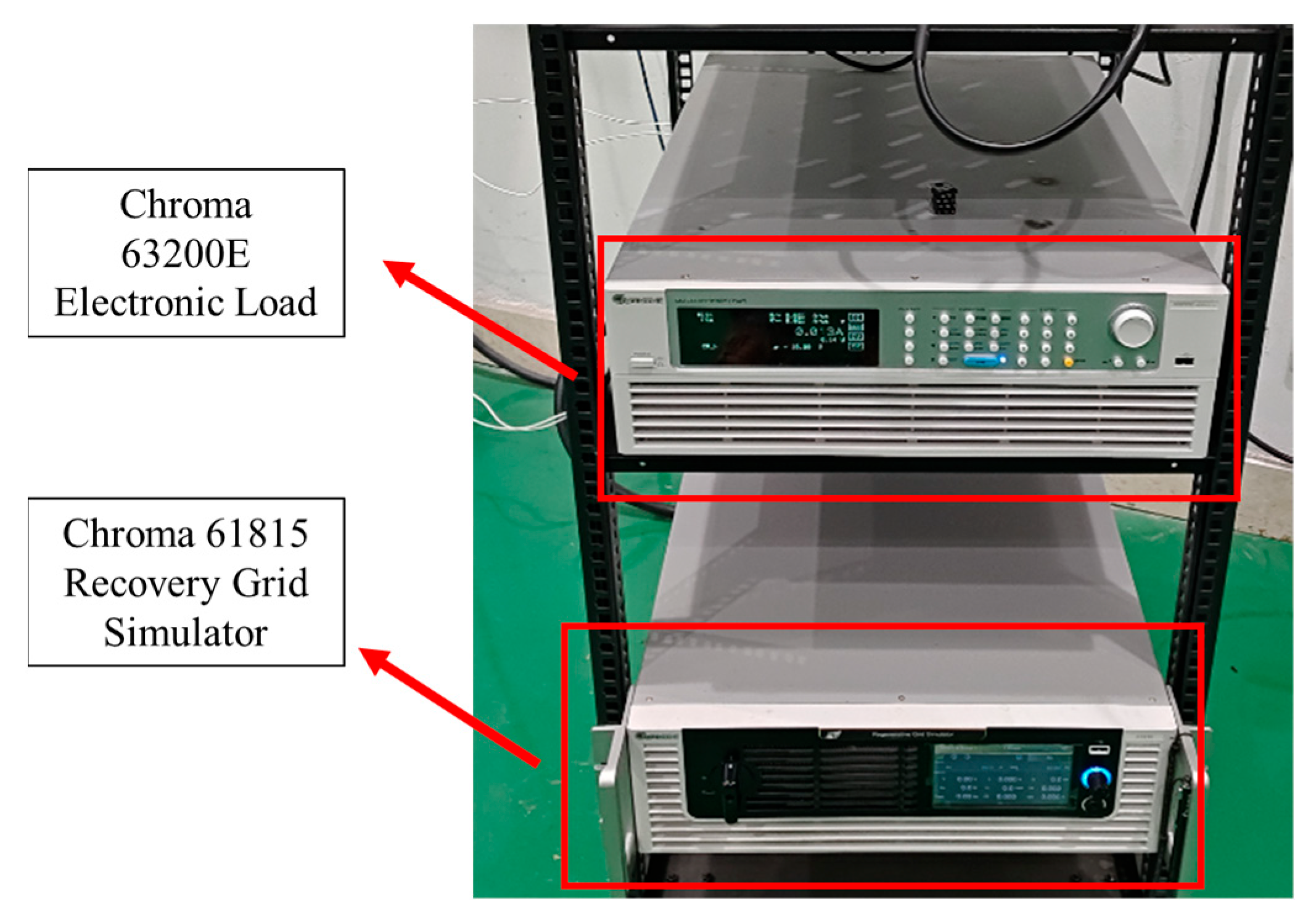
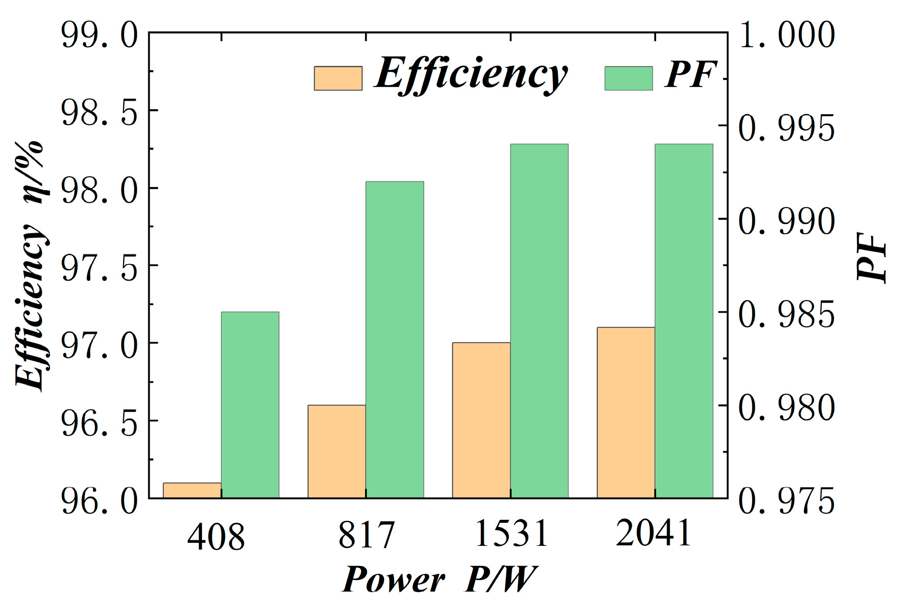
5.2. Electronic Load
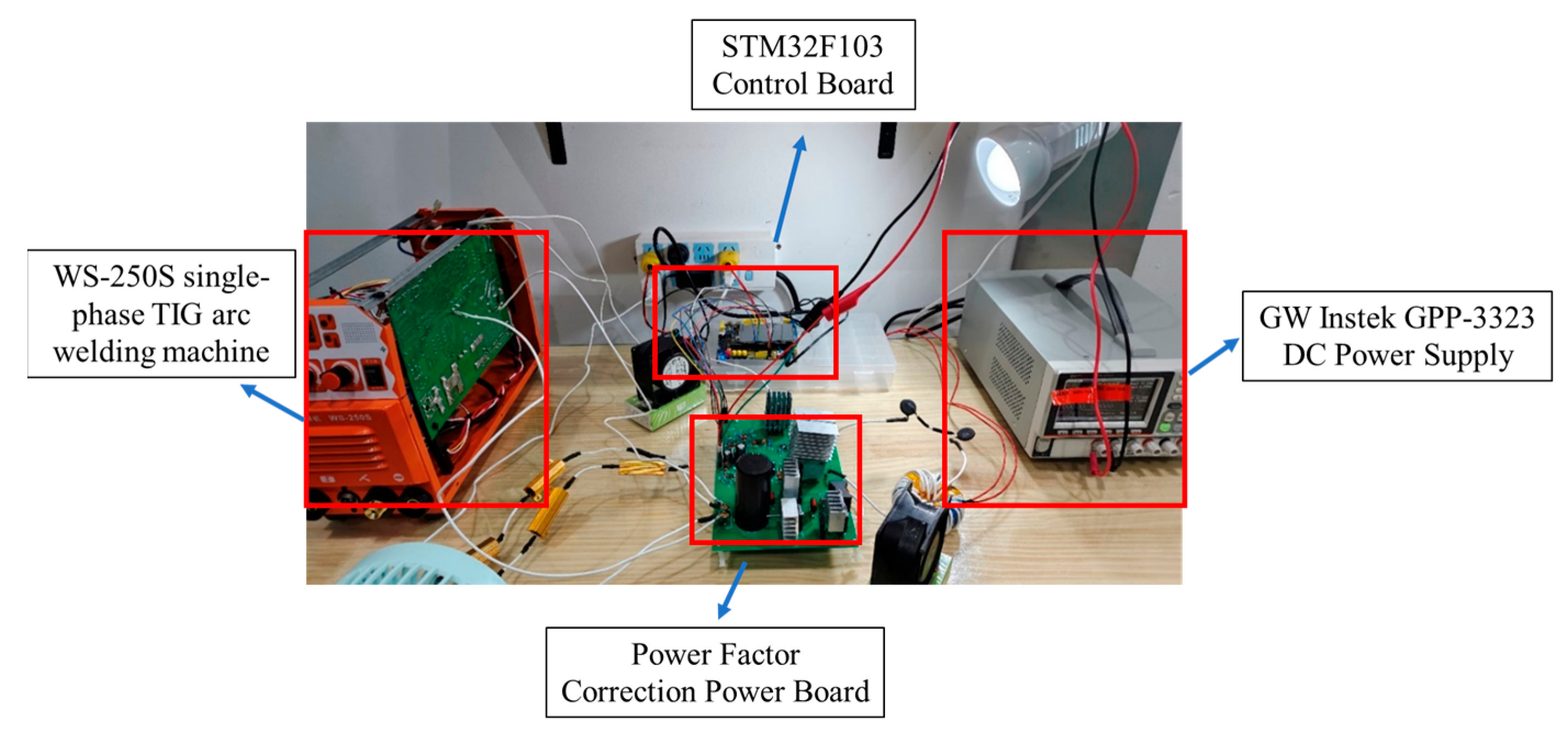
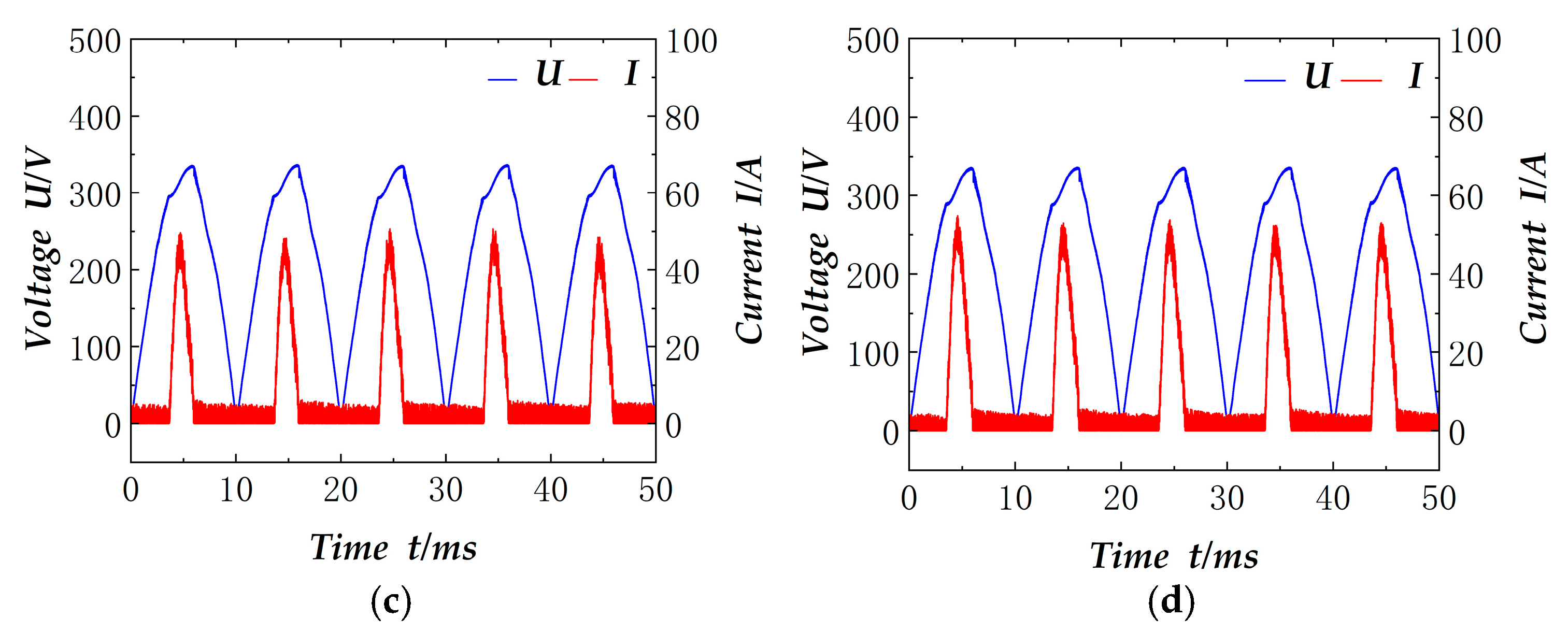
5.3. Welding Test
6. Conclusions
- The soft switching test was selected for three different moments within a single cycle, all of which were verified, and the results showed that the soft switching goal was achieved.
- The electronic load results show that, for the power from 500 W to 2000 W, the power factor correction can be more than 0.985, and the circuit efficiency can be more than 96%.
- For the TIG welding current of 30 A to 110 A, the power factor is up to 0.99, and the inner loop current control fluctuation is slightly larger than the electronic load.
Author Contributions
Funding
Institutional Review Board Statement
Informed Consent Statement
Data Availability Statement
Conflicts of Interest
References
- Huang, S.; Wu, X.; Wang, Z.; Wang, Z. New Development of Modern Welding Power. China Mech. Eng. 2002, 13, 1253–1256. [Google Scholar]
- Choi, S.-W.; Oh, S.-T.; Kim, M.-W.; Lee, I.-O.; Lee, J.-Y. Interleaved Isolated Single-Phase PFC Converter Module for Three-Phase EV Charger. IEEE Trans. Veh. Technol. 2020, 69, 4957–4967. [Google Scholar] [CrossRef]
- GB 28736-2019; Minimum Allowable Values of Energy Efficiency and Energy Efficiency Grades for Welding Machine. China Standard Press: Beijing, China, 2019.
- Ko, W.-H.; Gu, J.-C. Design and application of a thyristor switched capacitor bank for a high harmonic distortion and fast changing single-phase electric welding machine. IET Power Electron. 2016, 9, 2751–2759. [Google Scholar] [CrossRef]
- Xue, S.; Wang, B.; Zhang, L.; Long, W. Development of Green Welding Technology in China During the Past Decade. Mater. Rev. 2019, 33, 2813–2830. [Google Scholar]
- Pipiska, M.; Frivaldsky, M.; Hudak, P. Dual Interleaved Power Factor Correction for Welding Inverter. In Proceedings of the 12th International Conference on Elektro, Mikulov, Czech Republic, 21–23 May 2018. [Google Scholar]
- Zhang, H.; Tang, L.; Sun, S.; Jiang, F.; Yang, K.; Li, D. A Design of Single Phase Converter with Active Power Factor Correction Module. In Proceedings of the 20th IEEE International Conference on Electrical Machines and Systems, Sydney, Australia, 11–17 August 2017. [Google Scholar]
- Xiao, G.L. Application of PFC Technology Based on UC3854 for Invert Welder. Autom. Inf. Eng. 2011, 32, 39–41. [Google Scholar]
- Ando, I.; Abe, K.; Nakamura, T.; Araki, Y.; Ohnishi, K. Soft-Switching Interleaved PFC Converter with Lossless Snubber. Electr. Eng. Jpn. 2017, 198, 106–115. [Google Scholar] [CrossRef]
- Huang, J.; Chen, S.; Yin, S.; Wang, D.; Zeng, H. PFC of Three Phases Arc Welding Inverter Controlled by a Digital Singal Processor. J. Peking Polytech. Univ. 2003, 29, 151–154. [Google Scholar]
- Madhulingam, T.; Subbaiyan, T.; Shanmugam, P.; Kannan, S. Design and development of improved power quality based micro-butt welding power supply. IET Power Electron. 2017, 10, 746–755. [Google Scholar] [CrossRef]
- Bellec, Q.; Le Claire, J.C.; Benkhoris, M.F.; Coulibaly, P. Power factor correction and DC voltage control limits for arc welding application using pulsed current. In Proceedings of the 44th Annual Conference of the IEEE Industrial-Electronics-Society (IECON), Washington, DC, USA, 20–23 October 2018. [Google Scholar]
- Irving, B.T.; Jovanovic, M.M. Analysis, design, and performance evaluation of flying-capacitor passive lossless snubber applied to PFC boost converter. In Proceedings of the 17th Annual IEEE Applied Power Electronics Conference and Exposition, Dallas, TX, USA, 10–14 March 2002. [Google Scholar]
- Kim, H.-S.; Baek, J.-W.; Ryu, M.-H.; Kim, J.-H.; Jung, J.-H. Passive Lossless Snubbers Using the Coupled Inductor Method for the Soft Switching Capability of Boost PFC Rectifiers. J. Power Electron. 2015, 15, 366–377. [Google Scholar] [CrossRef]
- Smith, K.M.; Smedley, K.M. Properties and synthesis of passive lossless soft-switching PWM converters. IEEE Trans. Power Electron. 1999, 14, 890–899. [Google Scholar] [CrossRef]
- Wu, H.Y.; He, X.N. Single phase three-level power factor correction circuit with passive lossless-snubber. IEEE Trans. Power Electron. 2002, 17, 946–953. [Google Scholar]
- Li, R.T.H.; Chung, H.S.H.; Sung, A.K.T. Passive Lossless Snubber with Minimum Voltage and Current Stress for Boost PFC. In Proceedings of the IEEE Energy Conversion Congress and Exposition, San Jose, CA, USA, 20–24 September 2009. [Google Scholar]
- Mamizadeh, A.; Genc, N. Performance Analysis of Meta-Heuristic Algorithms for Optimal PI Tuning of PFC. Electr. Power Compon. Syst. 2024, 52, 1039–1053. [Google Scholar] [CrossRef]
- Janakiraman; Babu, R. Closed Loop Speed Controlled Two Stage PFC Converter Fed PMSM Drive. In Proceedings of the Conference on Innovations in Power and Advanced Computing Technologies, Vellore, India, 21–22 April 2017. [Google Scholar]
- Haber, R.; Rossiter, J.A.; Zabet, K. An Alternative for PID control: Predictive Functional Control—A Tutorial. In Proceedings of the American Control Conference, Boston, MA, USA, 6–8 July 2016. [Google Scholar]
- Wang, B.; Zheng, T.Q.; Zhang, J. Further reduction of switching loss for the lossless snubber based converters. In Proceedings of the 2014 IEEE Energy Conversion Congress and Exposition. Pittsburgh, PA, USA, 14–18 September 2014. [Google Scholar]
- Giaouris, D.; Banerjee, S.; Zahawi, B.; Pickert, V. Control of Fast Scale Bifurcations in Power-Factor Correction Converters. IEEE Trans. Circuits Syst. II Express Briefs 2007, 54, 805–809. [Google Scholar] [CrossRef]
- Choi, Y.; Kim, T.; Kim, R. An Active Partial Switching Method in Tertiary Loop for a High-Efficiency Predictive Current-Mode Control PFC Converter. IEEE Trans. Ind. Electron. 2018, 65, 7818–7828. [Google Scholar] [CrossRef]


Disclaimer/Publisher’s Note: The statements, opinions and data contained in all publications are solely those of the individual author(s) and contributor(s) and not of MDPI and/or the editor(s). MDPI and/or the editor(s) disclaim responsibility for any injury to people or property resulting from any ideas, methods, instructions or products referred to in the content. |
© 2025 by the authors. Licensee MDPI, Basel, Switzerland. This article is an open access article distributed under the terms and conditions of the Creative Commons Attribution (CC BY) license (https://creativecommons.org/licenses/by/4.0/).
Share and Cite
Lv, X.; Jiang, M. Design on Power Factor Correction of a Digital Soft Switching Single-Phase Arc Welding Power Source. Materials 2025, 18, 2138. https://doi.org/10.3390/ma18092138
Lv X, Jiang M. Design on Power Factor Correction of a Digital Soft Switching Single-Phase Arc Welding Power Source. Materials. 2025; 18(9):2138. https://doi.org/10.3390/ma18092138
Chicago/Turabian StyleLv, Xiaoqing, and Minhao Jiang. 2025. "Design on Power Factor Correction of a Digital Soft Switching Single-Phase Arc Welding Power Source" Materials 18, no. 9: 2138. https://doi.org/10.3390/ma18092138
APA StyleLv, X., & Jiang, M. (2025). Design on Power Factor Correction of a Digital Soft Switching Single-Phase Arc Welding Power Source. Materials, 18(9), 2138. https://doi.org/10.3390/ma18092138