

Diamond Wire Wear and Its Effect on Surface Quality in Cutting of Monocrystalline Silicon


 ,
, 
Abstract
1. Introduction
2. Experimental Methods
2.1. Experimental Equipment
2.2. Design of Experiments
2.2.1. Experimental Design for Diamond Wire Machining of Monocrystalline Silicon with Different Areas
2.2.2. Experimental Design for Diamond Wire Wear
3. Results and Discussion
3.1. Diamond Wire Wear Analysis
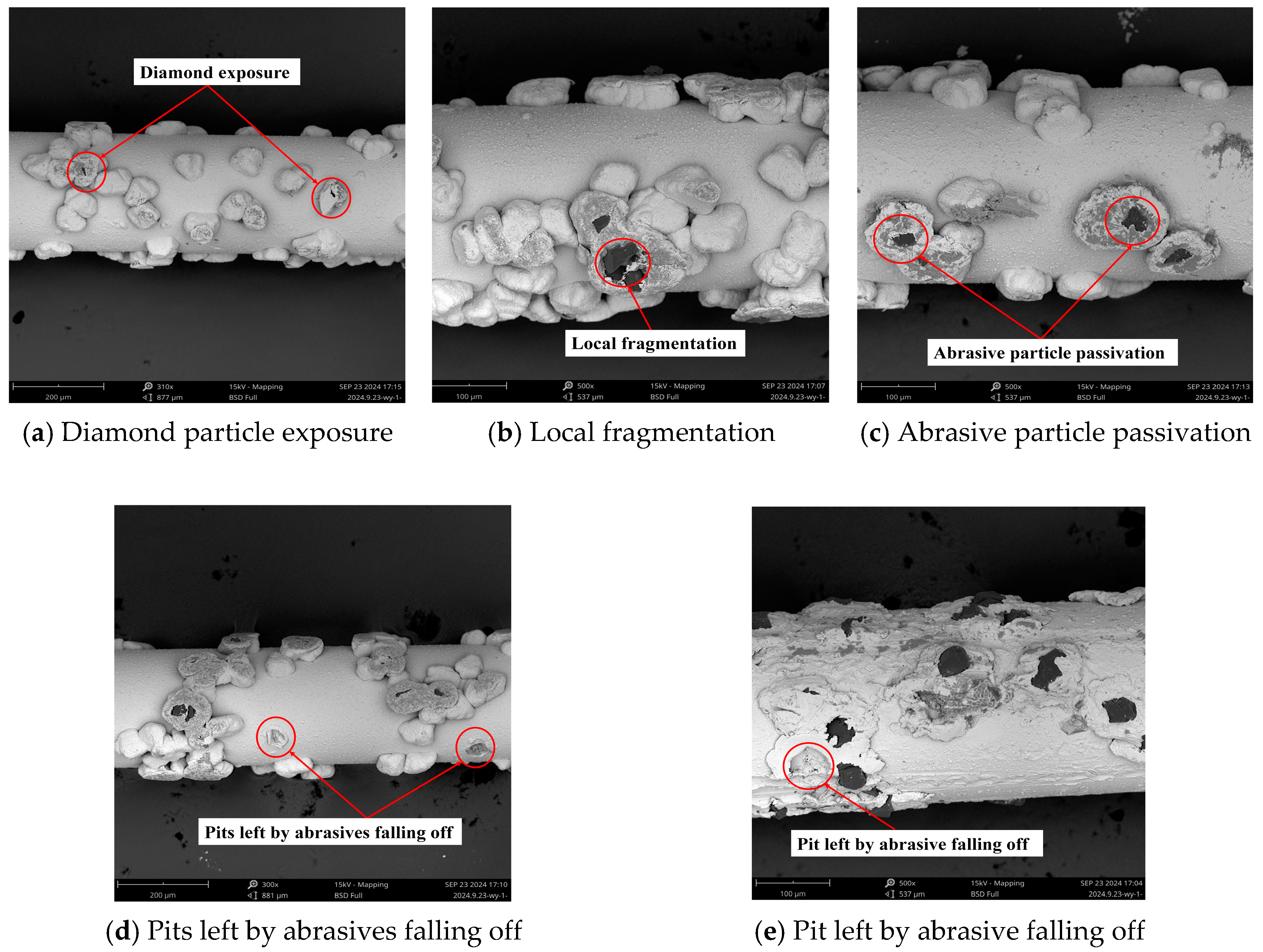
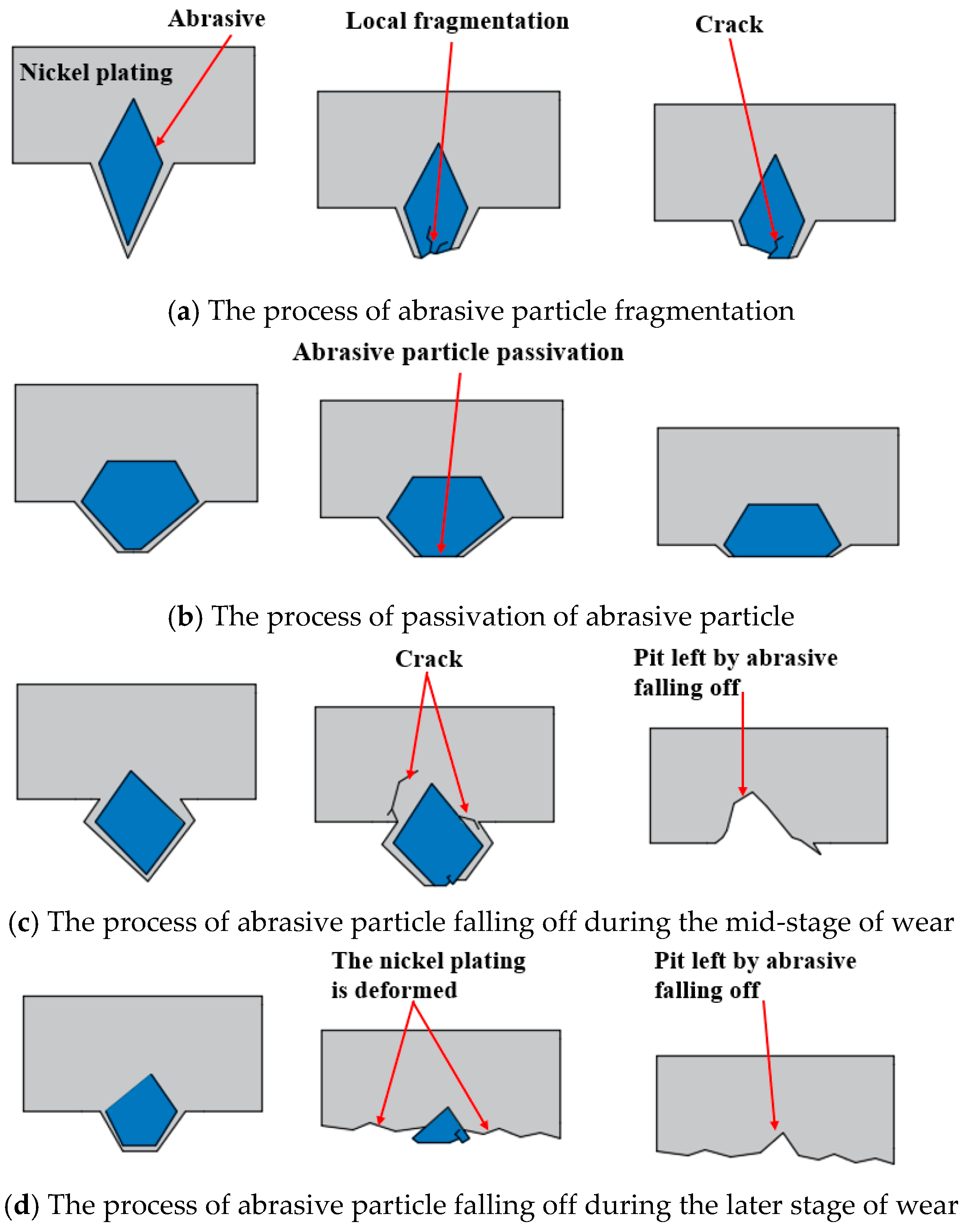
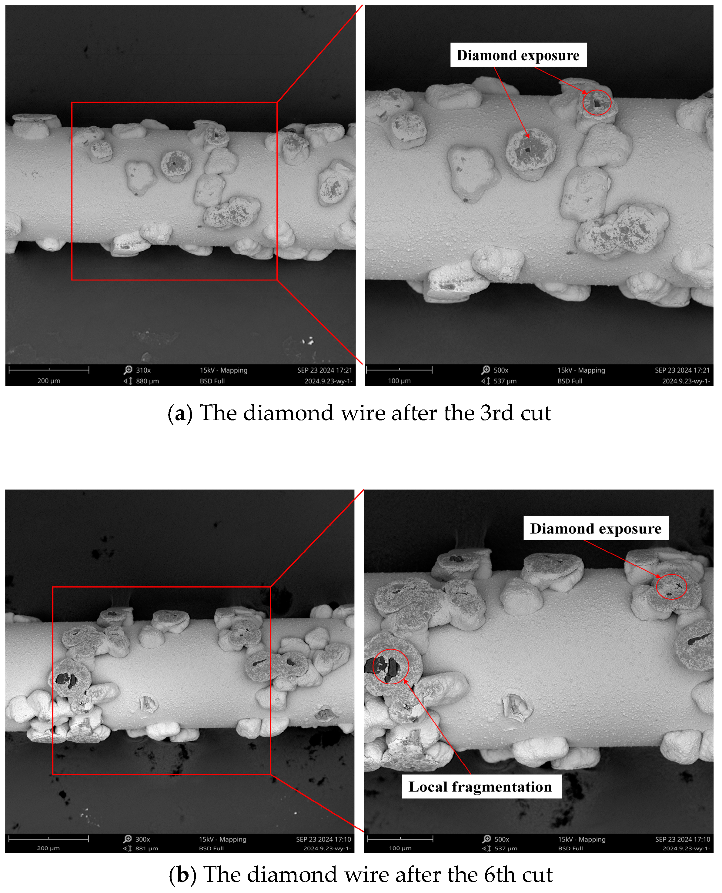
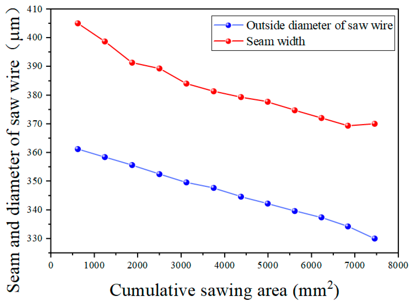
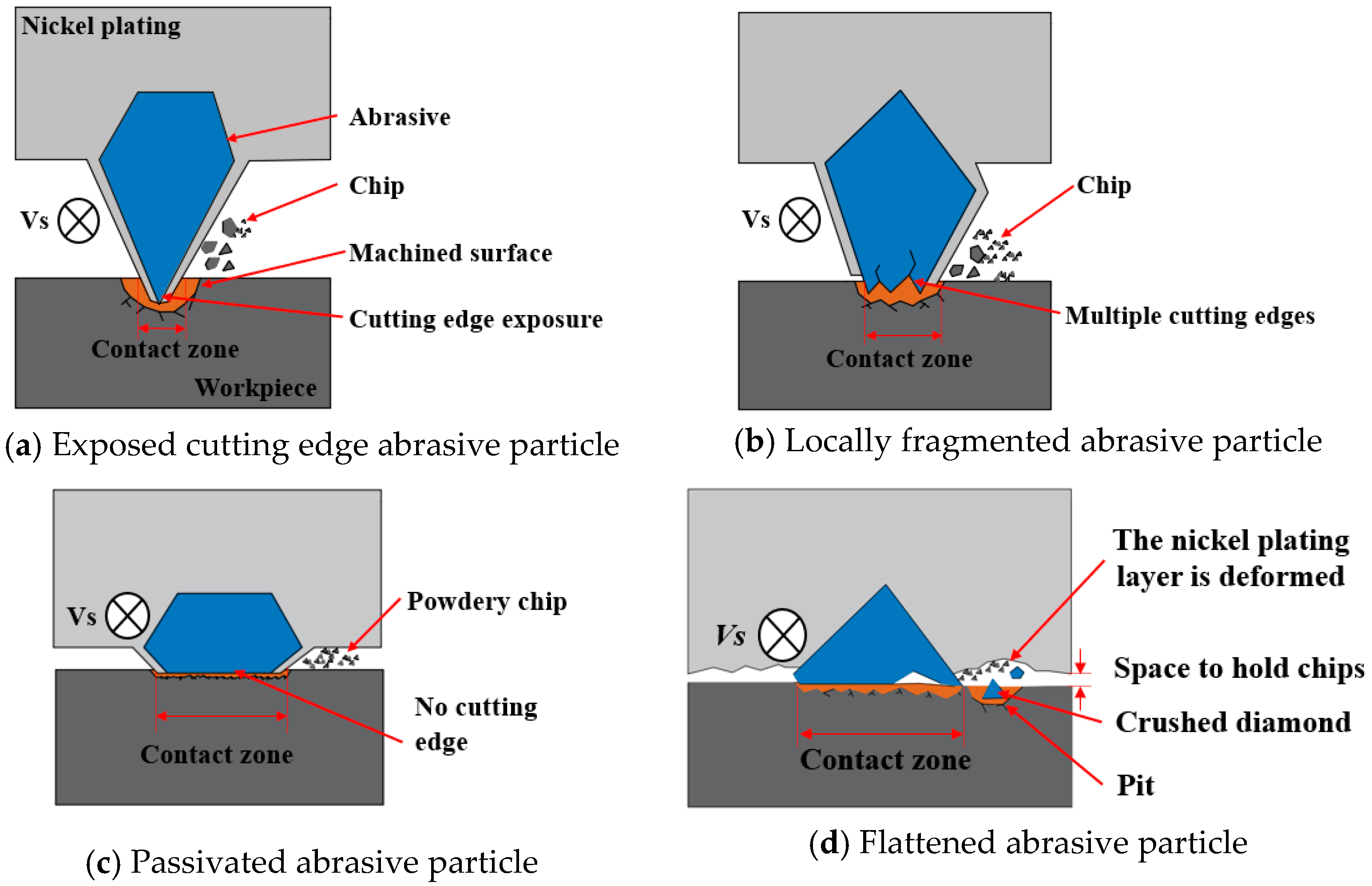
3.1.1. Wear Morphology and Wear Rate of Diamond Wire
- (1)
- Study on the wear of abrasive particles
- (2)
- Wear morphology of diamond wire
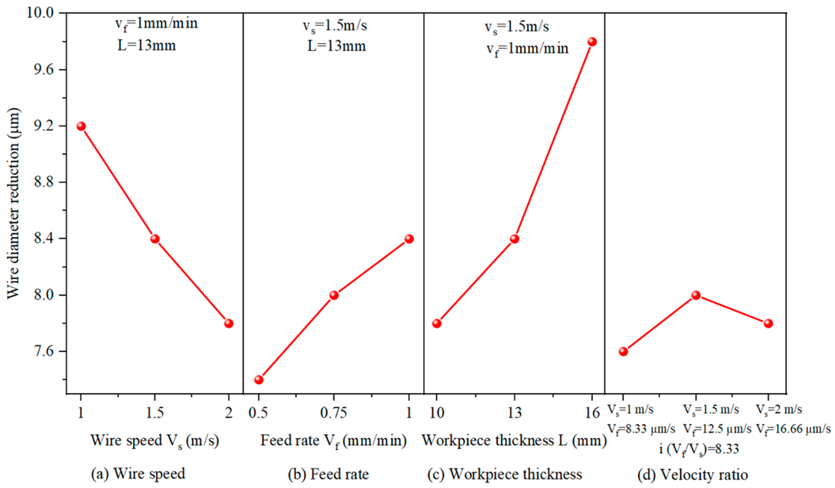
3.1.2. Effect of Machining Parameters on Diamond Wire Wear
3.2. Effect of Diamond Wire Wear on the Machining Quality of Monocrystalline Silicon
3.2.1. Effect of Diamond Wire Wear on the Total Thickness Variation (TTV) of Wafers
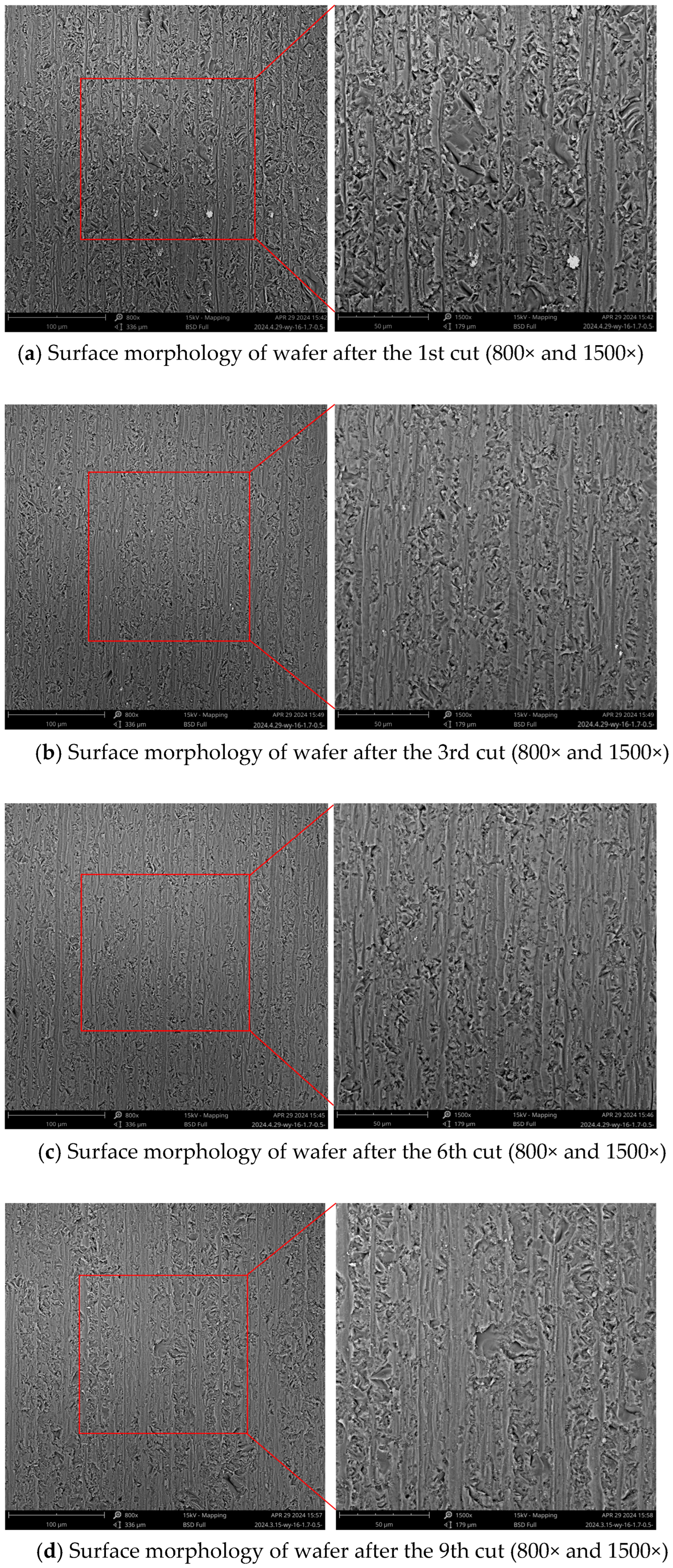
3.2.2. Effect of Diamond Wire Wear on Surface Quality of Wafers
4. Conclusions
- (1)
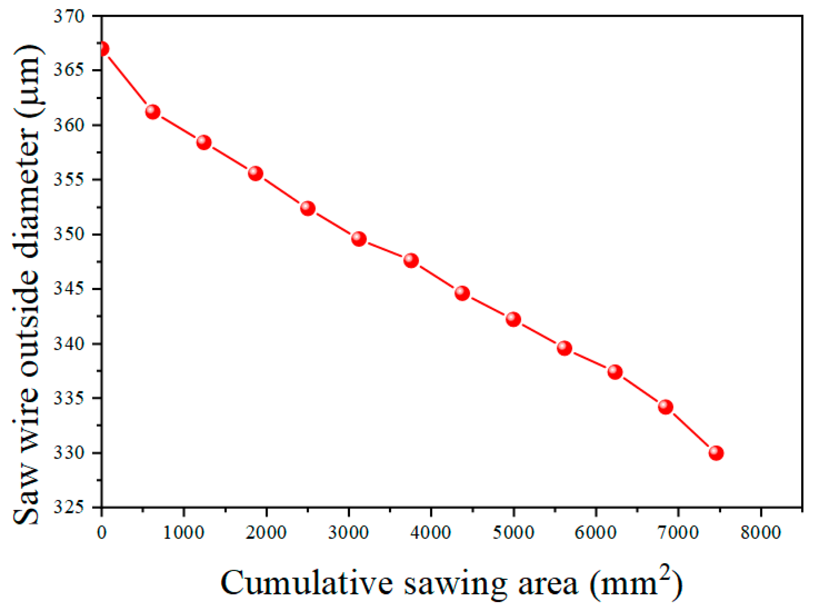
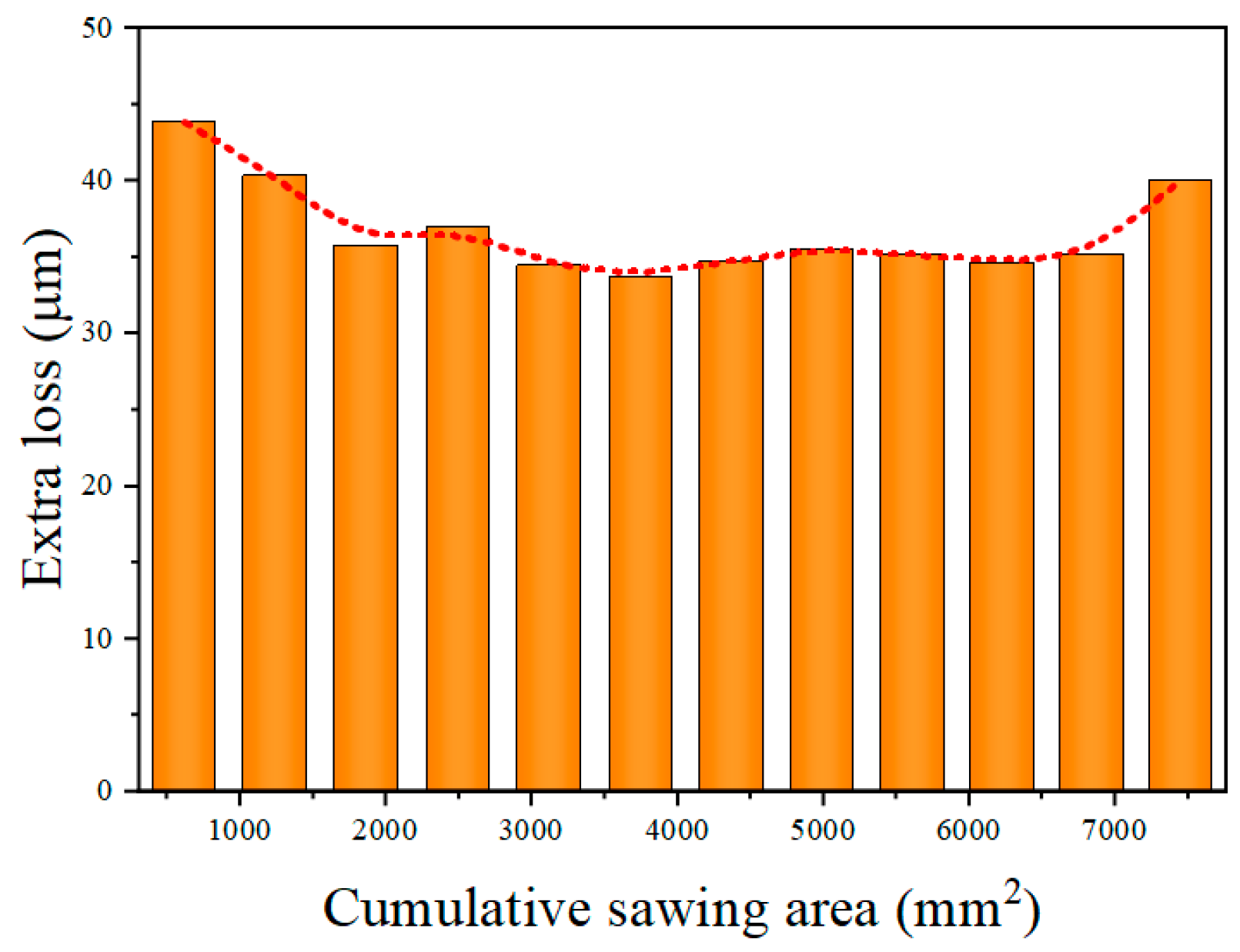
- The wear rate of the diamond wire was highest at the start of cutting, with the wear rate of the first cut reaching up to 9.374 × 10⁻⁶ mm−1. It remained low during the middle wear stage, where the wear rate of the sixth cut was only 3.185 × 10⁻⁶ mm−1. However, it increased again during the later wear stage, reaching 6.864 × 10⁻⁶ mm−1 at the 12th cut. The morphology of the abrasive particles after wear can be categorized into four types: diamond particle exposure, local fragmentation, abrasive particle passivation, and detachment of the abrasive particle. In addition, abrasive particle detachment not only occurred in the later stages of wear but also during the middle stage of wear when the abrasive particle density on the surface of the saw wire was low or when it was subjected to large force.
- (2)
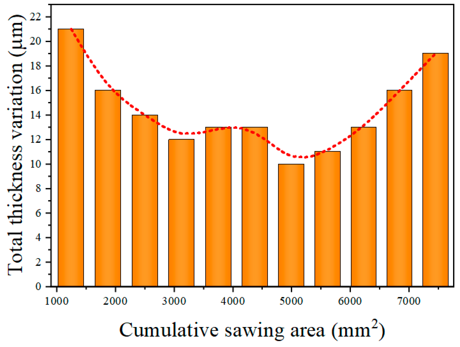
- In the early stage of diamond wire wear, the TTV of the wafer was relatively large, reaching 21 μm during the second cut. In the middle wear stage of the diamond wire, the TTV was smaller, being only 10 μm during the eighth cut. In the later stage of wear, the TTV began to increase, reaching 19 μm during the 12th cut. Changes in the extra loss affected the TTV of the wafer. During the steady wear state, the fluctuation in extra loss was small, bringing about a low TTV for the silicon wafer.
- (3)
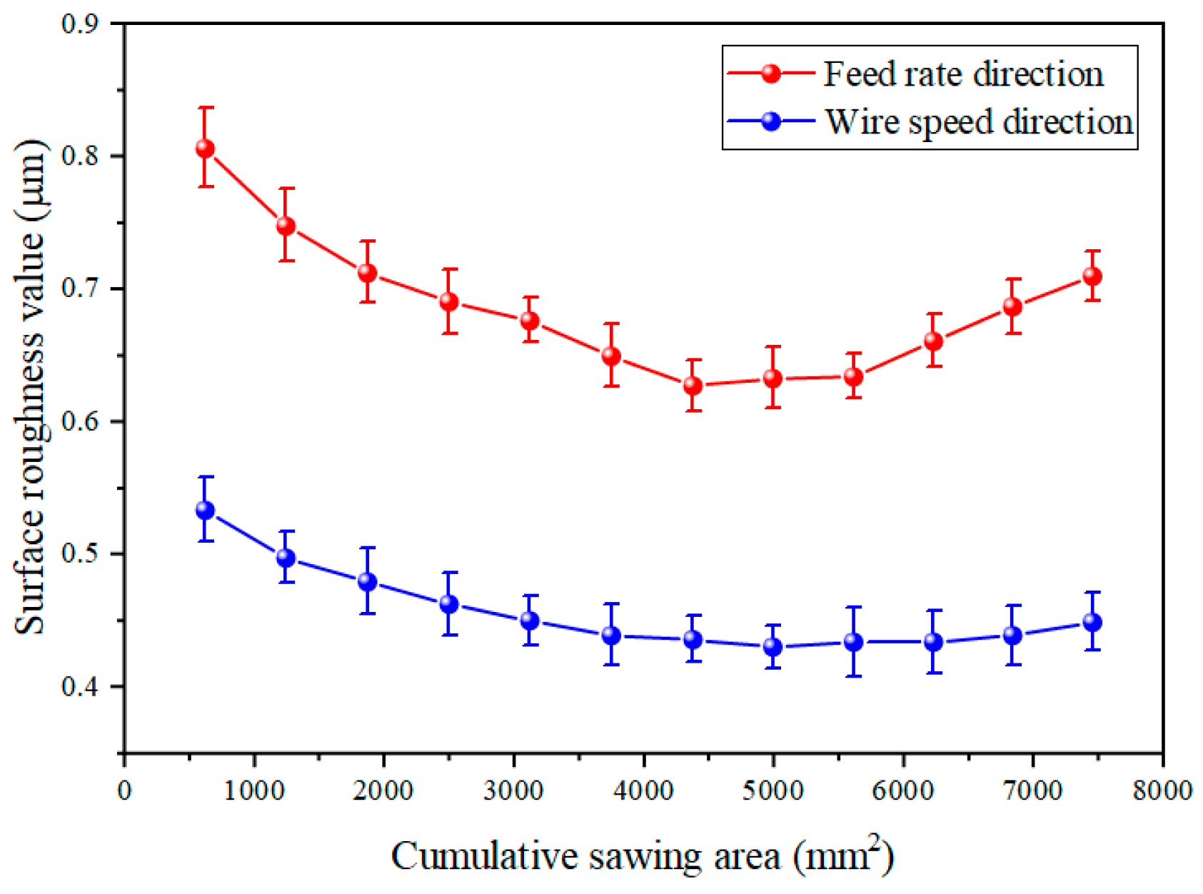
- As the machining area of the diamond wire increased, the Ra value of the monocrystalline silicon wafers displayed a trend of initially declining, followed by an increase. As the wear of the saw wire occurred, the surface roughness value in the wire velocity direction decreased from 0.533 μm to 0.43 μm and then increased to 0.449 μm. In the feed direction, the surface roughness value decreased from 0.806 μm to 0.627 μm and then increased to 0.71 μm. In the early stage of wear, the surface of the wafer exhibited more brittle pits. In the period of stable wear, the silicon wafer showed less brittle removal and more ductility removal, while the surface defects increased in the later wear stage.
- (4)
- When using different machining parameters to cut the same wafer area, the results indicate that diamond wire wear declines with an increase in wire velocity, rises with an increase in the feed rate, and rises with an increase in the cutting thickness of the wafer. When both the feed rate and the wire velocity increased but maintained their ratio, the diamond saw wear remained basically unchanged.
Author Contributions
Funding
Institutional Review Board Statement
Informed Consent Statement
Data Availability Statement
Conflicts of Interest
References
- Ge, M.; Zhang, C.; Wang, P.; Li, Z.; Ge, P. Modeling of electroplated diamond wire and its application towards precision slicing of semiconductors. J. Manuf. Process. 2023, 87, 141–149. [Google Scholar] [CrossRef]
- Wu, H.; Yang, C.; Melkote, S.N. Effect of reciprocating wire slurry sawing on surface quality and mechanical strength of as-cut solar silicon wafers. Precis. Eng. 2014, 38, 121–126. [Google Scholar] [CrossRef]
- Wang, Z.; Ren, Y.; Ma, W.; Lv, G.; Tan, M.; Li, X.; Li, S.; Wan, X.; Zhan, S.; Zeng, Y.; et al. Crystal surface heat transfer during the growth of 300mm monocrystalline silicon by the Czochralski process. Int. J. Heat Mass Transf. 2025, 236, 126259. [Google Scholar] [CrossRef]
- Li, Z. Prospects of photovoltaic technology. Engineering 2023, 21, 28–31. [Google Scholar] [CrossRef]
- Cheng, D.; Gao, Y.; Li, G. Fracture strength analysis of large-size and thin photovoltaic monocrystalline silicon wafers. Eng. Fract. Mech. 2024, 310, 110523. [Google Scholar] [CrossRef]
- Kumar, A.; Melkote, S.N. Diamond wire sawing of solar silicon wafers: A sustainable manufacturing alternative to loose abrasive slurry sawing. Procedia Manuf. 2018, 21, 549–566. [Google Scholar] [CrossRef]
- Murthy, H.S.G.K. Evolution and present status of silicon carbide slurry recovery in silicon wire sawing. Resour. Conserv. Recycl. 2015, 104, 194–205. [Google Scholar] [CrossRef]
- Gao, Y.; Ge, P.; Liu, T. Experiment study on electroplated diamond wire saw slicing single-crystal silicon. Mater. Sci. Semicond. Process 2016, 56, 106–114. [Google Scholar] [CrossRef]
- Wallburg, F.; Kuna, M.; Budnitzki, M.; Schoenfelder, S. Experimental and numerical analysis of scratching induced damage during diamond wire sawing of silicon. Wear 2020, 454, 203328. [Google Scholar] [CrossRef]
- Li, A.; Hu, S.; Zhou, Y.; Wang, H.; Zhang, Z.; Ming, W. Recent advances in precision diamond wire sawing monocrystalline silicon. Micromachines 2023, 14, 1512. [Google Scholar] [CrossRef]
- Wang, Y.; He, S.; Chen, Y.; Jiang, C.; Qian, Z.; Chen, H. Mechanism analysis and experimental verification of ultrasonic cavitation assisted diamond wire saw cutting monocrystalline silicon. Engl. Ed. 2024, 60, 114–126. [Google Scholar]
- Cheng, D.; Gao, Y. Effect of the diamond saw wires capillary adhesion on the thickness variation of ultra-thin photovoltaic silicon wafers during slicing. Sol. Energy Mater. Sol. Cells 2023, 261, 112525. [Google Scholar] [CrossRef]
- Sefene, E.M.; Chen, C.C.A.; Lien, H.C. Enhancing sustainability and machinability in electrophoretic-assisted diamond wire sawing of monocrystalline silicon wafer. J. Manuf. Process. 2024, 131, 1531–1547. [Google Scholar] [CrossRef]
- Wang, Y.; Xu, K.; Xue, H.; Li, J.; Li, Y. Anisotropic mechanism of monocrystalline silicon on surface quality in precision diamond wire saw cutting. Mater. Sci. Semicond. Process. 2025, 185, 108961. [Google Scholar] [CrossRef]
- Lottspeich, L.; Theophil, L.; Fuchs, M.; Kaden, T. A novel approach to determine the diamond occupancy of diamond wires for optimized cutting processes for crystalwire silicon. In Proceedings of the 33rd European Photovoltaic Solar Energy Conference and Exhibition, Amsterdam, The Netherlands, 25–29 September 2017; pp. 530–533. [Google Scholar]
- Li, Z.; Wang, M.; Pan, X.; Ni, Y. Slicing parameters optimizing and experiments based on constant wire wear loss model in multi-wire saw. Int. J. Adv. Manuf. Technol. 2015, 81, 29–334. [Google Scholar] [CrossRef]
- Hsu, C.Y.; Chen, C.S.; Tsao, C.C. Free abrasive wire saw machining of ceramics. Int. J. Adv. Manuf. Technol. 2009, 40, 503–511. [Google Scholar] [CrossRef]
- Meng, J.; Li, J.; Ge, P.; Zhou, R. Research on endless wire saw cutting of Al2O3/TiC ceramics. Key Eng. Mater. 2006, 315, 571–574. [Google Scholar] [CrossRef]
- Lee, S.; Kim, H.; Kim, D.; Park, C. Investigation on diamond wire break-in and its effects on cutting performance in multi-wire sawing. Int. J. Adv. Manuf. Technol 2016, 87, 1–8. [Google Scholar] [CrossRef]
- Banerjee, S.; Yang, J.; Wu, J.; Wu, J.; Heredia, M.; Gao, Z.; Myung, Y.; Rezvanian, O.; Banerjee, P. Phase and stress evolution of Si swarf in the diamond-coated wire sawing of Si ingots. Int. J. Adv. Manuf. Technol. 2017, 89, 735–742. [Google Scholar] [CrossRef]
- Peguiron, J.; Mueller, R.; Zanetti, J.; Habegger, S.; Burri, M.; Sopra, F.M. Reducing wire wear by mechanical optimization of equipment in diamond-wire wafering. PV Prod. Annu. 2014, 1–9. [Google Scholar]
- Knoblauch, R.; Boing, D.; Weingaertner, W.L.; Wegener, K.; Kuster, F.; Xavier, F.A. Investigation of the progressive wear of individual diamond grains in wire used to cut monocrystalline silicon. Wear 2018, 414, 50–58. [Google Scholar] [CrossRef]
- Gao, W.; Zhang, J.; Duan, J. Study on the wear topography of diamond endless wire saw when cutting granite. Key Eng. Mater. 2011, 487, 361–365. [Google Scholar] [CrossRef]
- Meißner, D.; Schoenfelder, S.; Hurka, B.; Zeh, J.; Sunder, K.; Koepge, R.; Wagner, T.; Grün, A.; Hagel, H.J.; Moeller, H.J. Loss of wire tension in the wire web during the slurry based multi wire sawing process. Sol. Energy Mater. Sol. Cells 2013, 120, 346–355. [Google Scholar] [CrossRef]
- Yang, J.; Banerjee, S.; Wu, J.; Myung, Y.; Rezvanian, O.; Banerjee, P. Phase and stress evolution in diamond microparticles during diamond-coated wire sawing of Si ingots. Int. J. Adv. Manuf. Technol. 2016, 82, 1675–1682. [Google Scholar] [CrossRef]
- Sekhar, H.; Fukuda, T.; Tanahashi, K.; Takato, H. The impact of silicon brick polishing on thin (120 μm) silicon wafer sawing yields and fracture strengths in diamond-wire sawing. Mater. Sci. Semicond. Process. 2020, 105, 104751. [Google Scholar] [CrossRef]
- Kumar, A.; Kaminski, S.; Melkote, S.N.; Arcona, C. Effect of wear of diamond wire on surface morphology, roughness and subsurface damage of silicon wafers. Wear 2016, 364, 163–168. [Google Scholar] [CrossRef]
- Suzuki, T.; Otsuki, T.; Yan, J.W. Study on precision slicing process of single-crystal silicon by using dicing wire saw. Adv. Mater. Res. 2016, 1136, 350–356. [Google Scholar] [CrossRef]
- Yin, Y.; Gao, Y.; Yang, C. Sawing characteristics of diamond wire cutting sapphire crystal based on tool life cycle. Ceram. Int. 2021, 47, 26627–26634. [Google Scholar] [CrossRef]
- Wang, Y.; Zhang, S.; Dong, G.; Su, J.; Qian, Z.; Zhou, J. Theoretical study on sawing force of ultrasonic vibration assisted diamond wire sawing (UAWS) based on abrasives wear. Wear 2022, 496, 204291. [Google Scholar] [CrossRef]
- Li, X.; Gao, Y.; Ge, P.; Zhang, L.; Bi, W. The effect of cut depth and distribution for abrasives on wafer surface morphology in diamond wire sawing of PV polycrystalline silicon. Mater. Sci. Semicond. Process. 2019, 91, 316–326. [Google Scholar] [CrossRef]
- Zhu, Z.; Gao, Y.; Shi, S.; Zhang, X. Study on surface characteristics of as-sawn sapphire crystal wafer considering diamond saw wire wear. Wear 2023, 530, 205037. [Google Scholar] [CrossRef]
- Pala, U.; Süssmaier, S.; Kuster, F.; Wegener, K. Experimental investigation of tool wear in electroplated diamond wire sawing of silicon. Procedia CIRP 2018, 77, 371–374. [Google Scholar] [CrossRef]
- Hardin, C.W.; Qu, J.; Shih, A.J. Fixed abrasive diamond wire saw slicing of single-crystal silicon carbide wafers. Mater. Manuf. Processes 2004, 19, 355–367. [Google Scholar] [CrossRef]
- Yin, Y.; Gao, Y.; Li, X.; Pu, T.; Wang, L. Experimental study on slicing photovoltaic polycrystalline silicon with diamond wire saw. Mater. Sci. Semicond. Process. 2019, 106, 104779. [Google Scholar] [CrossRef]


| Description | Diamond Wire A | Diamond Wire B |
|---|---|---|
| Diameter of wire (μm) | 350 | 250 |
| Average abrasive size (μm) | 30–40 | 20–30 |
| Length of diamond wire (m) | 20 | 20 |
| Experiment | Exp. I | Exp. II | Exp. III | Exp. IV |
|---|---|---|---|---|
| Wafer (pieces) | 3 | 6 | 9 | 12 |
| Cutting time (min) | 180 | 360 | 540 | 720 |
| Machining Parameter | Exp. I | Exp. II | Exp. III |
|---|---|---|---|
| Wire velocity Vs (m/s) | 1, 1.5, 2 | 1.5 | 1.5 |
| Feed rate Vf (mm/min) | 1 | 0.5, 0.75, 1 | 1 |
| Workpiece thickness L (mm) | 13 | 13 | 10, 13, 16 |
| Machining Parameter | Exp. I | Exp. II | Exp. III |
|---|---|---|---|
| Wire velocity Vs (m/s) | 1 | 1.5 | 2 |
| Feed rate Vf (mm/min) | 8.33 | 12.5 | 16.66 |
| Workpiece thickness L (mm) | 13 | 13 | 13 |
| Velocity ratio (μm/m) | 8.33 | 8.33 | 8.33 |
Disclaimer/Publisher’s Note: The statements, opinions and data contained in all publications are solely those of the individual author(s) and contributor(s) and not of MDPI and/or the editor(s). MDPI and/or the editor(s) disclaim responsibility for any injury to people or property resulting from any ideas, methods, instructions or products referred to in the content. |
© 2025 by the authors. Licensee MDPI, Basel, Switzerland. This article is an open access article distributed under the terms and conditions of the Creative Commons Attribution (CC BY) license (https://creativecommons.org/licenses/by/4.0/).
Share and Cite
Du, J.; Wu, Y.; Zhang, Z.; Zhang, Y.; He, W.; Geng, J.; Duan, L.; Ming, W. Diamond Wire Wear and Its Effect on Surface Quality in Cutting of Monocrystalline Silicon. Materials 2025, 18, 1768. https://doi.org/10.3390/ma18081768
Du J, Wu Y, Zhang Z, Zhang Y, He W, Geng J, Duan L, Ming W. Diamond Wire Wear and Its Effect on Surface Quality in Cutting of Monocrystalline Silicon. Materials. 2025; 18(8):1768. https://doi.org/10.3390/ma18081768
Chicago/Turabian StyleDu, Jinguang, Yu Wu, Zhen Zhang, Yu Zhang, Wenbin He, Junxiao Geng, Liuyang Duan, and Wuyi Ming. 2025. "Diamond Wire Wear and Its Effect on Surface Quality in Cutting of Monocrystalline Silicon" Materials 18, no. 8: 1768. https://doi.org/10.3390/ma18081768
APA StyleDu, J., Wu, Y., Zhang, Z., Zhang, Y., He, W., Geng, J., Duan, L., & Ming, W. (2025). Diamond Wire Wear and Its Effect on Surface Quality in Cutting of Monocrystalline Silicon. Materials, 18(8), 1768. https://doi.org/10.3390/ma18081768