Article

The Material Growth and Characteristics of Transition Metal Oxide Thin Films Based on Hot Wire Oxidation Sublimation Deposition Technology

1
School of Semiconductor and Physics, North University of China, Taiyuan 030051, China
2
State Key Laboratory of Widegap Semiconductor Optoelectronic Materials and Technologies, North University of China, Taiyuan 030051, China
3
State Key Laboratory of Extreme Environment Optoelectronic Dynamic Measurement Technology and Instrument, North University of China, Taiyuan 030051, China
*
Authors to whom correspondence should be addressed.
Materials 2025, 18(17), 4083; https://doi.org/10.3390/ma18174083
Submission received: 21 July 2025 / Revised: 15 August 2025 / Accepted: 26 August 2025 / Published: 31 August 2025
(This article belongs to the Section Thin Films and Interfaces)

Abstract

Transition-metal oxides (TMOs) possess pronounced optoelectronic properties and are widely exploited in photovoltaics and photocatalysis. Here, we introduce a hot wire oxidation sublimation deposition (HWOSD) that directly converts elemental Mo and W into amorphous MoOx and WOx films on various substrates. Scanning electron microscopy and atomic force microscopy reveal uniform thickness and conformal coverage over textured and planar surfaces. X-ray photoelectron spectroscopy indicates high oxygen contents with stoichiometric ratios of 2.94 (MoOx) and 2.91 (WOx). Optical measurements show transmittances > 94% across 400–1200 nm, yielding optical band gaps of 1.86 eV (MoOx) and 2.67 eV (WOx). The conductivities of MoOx and WOx were 2.58 × 10⁻⁶ S cm−1 and 5.14 × 10⁻⁷ S cm−1 at room temperature, and the TMO/Si surface potential differences are 200 mV and 114 mV, respectively. Minority-carrier-lifetime measurements indicate that MoOx films confer an additional passivation benefit to the i a-Si:H/c-Si/i a-Si:H stack. Annealing of MoOx and WOx realized their phase transition from an amorphous state to a polycrystalline state, with changes in their optical transmittance in the visible light region. Investigation of the photovoltaic performances of MoOx and WOx as HTLs deposited by HWOSD demonstrates their excellent electronic functionality in optoelectronics. These results establish HWOSD as a scalable, low-temperature method to fabricate high-quality TMO films and expand their potential in advanced optoelectronic devices.

1. Introduction

Transition metal oxides (TMOs) possess tunable energy bands, excellent light absorption capabilities, high carrier mobility, and wide spectral absorption, which have great potential in photovoltaics, photocatalysis, and electronic devices [1,2,3]. The conduction-band bottom of the TMO is sufficiently negative and its valence-band top appropriately positive, jointly satisfying the requirements for hydrogen and oxygen evolution [4,5]. Moreover, TMOs exhibit exceptional chemical robustness, rendering them highly suitable for sustained photocatalytic water splitting [6]. The high specific capacity and rapid charge transport enhance the energy density and cycle life of supercapacitors [7,8,9]. TMOs can also achieve rapid and reversible coloration under an electric field [10,11,12], improving the durability of electrochromic devices. In photovoltaics, TMO thin films, characterized by a near-optimal band gap, high optical transmittance, and outstanding thermal stability, serve as an ideal selective transport layer in solar cells [13,14]. Consequently, achieving high-quality TMOs has become a key technology for further advancing photovoltaics, photocatalysis, and electronic devices.
Within the realm of TMOs-enabled applications, molybdenum oxide (MoOx) and tungsten oxide (WOx) have garnered substantial research interest due to their unique physicochemical properties. MoOx is an indirect bandgap with a bandgap of 2.9–3.2 eV [15]. Its work function reaches 6.8 eV, increasing with the increase of the oxygen/molybdenum ratio [16]. WOx is also an indirect bandgap semiconductor with a relatively wide bandgap (3.2 eV) and is n-type, exhibiting high chemical stability and high conductivity [17,18]. And it can also be achieved by combining amorphous tungsten oxide with crystalline tungsten oxide to form a WO3 film. The high cycle stability of crystalline WO3 and the high ion storage and transmission capacity of amorphous WO3 can be utilized to enhance the overall performance and work function of the film [19,20].
The properties of TMO thin films in electronic materials are largely influenced by the deposition methods, including magnetron sputtering [21], thermal evaporation [22], and the sol-gel method [23], hot wire oxidation-sublimation [24,25,26,27], etc. In an O2/Ar plasma, a WO3 film was deposited by 60 W RF magnetron sputtering of a W target. XRD showed that it was in the hexagonal phase (100) and (200). WO3 films with different morphologies can be fabricated by using magnetron sputtering technology combined with oblique angle deposition technology. According to the UPS analysis, the deviation of the base position led to a decrease in the work function, and this resulted in an increase in the minimum value of the conduction band that approaches the reduction potential [27]. MoOx films were deposited by RF reactive magnetron sputtering at 4 mTorr while varying O2 flow, whose XPS confirmed increased stoichiometry with higher oxygen content, raising the work function to 5.92 eV, the highest yet reported for reactively sputtered MoOx [28]. Although magnetron sputtering routinely delivers dense, high-quality TMO films, the accompanying plasma bombardment frequently inflicts subtle substrate damage, elevating interfacial defect densities and, consequently, compromising ultimate device performance.
A 200 nm WO3 film was deposited at room temperature by thermal evaporation and subsequently annealed at 200, 400, and 500 °C for 1 h. X-ray diffraction confirmed the emergence of a highly oriented orthorhombic phase with preferential (001) orientation, UV–vis and photoluminescence spectroscopy revealed a progressive narrowing of the optical band gap from 3.25 eV to 2.60 eV [29]. The thermal evaporation has enabled the growth of uniform MoOx films on quartz and glass substrates, which were found to have amorphous characteristics by XRD analysis [30]. Thermal evaporation mitigates plasma-induced substrate damage, yet the inevitable pellet agglomeration of transition-metal-oxide powders tends to reduce both growth rate and source utilization, while subtly lowering the TMO work function.
Using hexachlorotungsten as the precursor, WO3 films were grown by the sol-gel method. Their structure, composition, and optical properties were characterized by SEM, XRD, and XPS. Cyclic voltammetry, chronoamperometry, and in-situ transmission measurements revealed that post-annealing the WO3 film attained an electrochemical reversibility of 0.81, substantially surpassing its as-deposited counterpart [31]. MoOx films were prepared by the sol-gel method using MoO3 powder and NH3 or H2O2 solution as precursors at room temperature. Then, they were directly treated with ultraviolet ozone without the need for high-temperature annealing. Through AFM, XPS, and UPS measurements, it was confirmed that the films were uniform, dense, had a stable chemical structure, and high work function [32]. While solution-based routes excel in process simplicity and cost-effectiveness, residuals from the precursors can increase interfacial trap densities and subtly compromise the TMO work function.
The hot-wire oxidation–sublimation deposition (HWOSD) demonstrates exceptional promise for fabricating transition-metal oxides. High-quality WOx films were fabricated via HWOSD by precisely regulating oxygen-vacancy density at 850 °C tungsten filament and 4–16 sccm O2, with XPS/UPS revealing a direct correlation between vacancy concentration and work function, enabling tunable values from 4.97 to 5.41 eV [24]. With increasing the oxygen flow ratio, the ratio of W6+ increases while W5+ decreases, concomitantly elevating the work function of WOx [25]. Prior investigations had already demonstrated the viability of the hot-wire oxidation–sublimation deposition (HWOSD) technique for synthesizing molybdenum oxide (MoOx) thin films [26]. Nevertheless, a systematic and comparative study that unifies the synthesis–structure–property relationships of HWOSD-grown WOx and MoOx remains absent, motivating the integrated investigation.
This work introduces a comprehensive and comparative account of HWOSD-enabled synthesis and in-depth characterization of WOx and MoOx thin films, whose morphology, electronic properties, and thermal stability were characterized by SEM, AFM, XPS, and XRD. The silicon heterojunction solar cells using MoOx or WOx as Hole selective transport layer were fabricated and showed excellent performance, offering robust theoretical guidance for TMO thin films deposition and its device application.

2. Experimental Details

2.1. Hot Wire Oxidation Sublimation Deposition

Hot wire oxidation sublimation deposition (HWOSD) was used to fabricate MoOx, and WOx, thin films, as shown in Figure 1: (a) In a vacuum chamber, oxygen and high temperature (in range of 600–1100 °C) hot wires of transition metals (such as: Mo and W) were reacted, generating their oxides on surfaces, which sublimated simultaneously and spread into the whole chamber in the form of molecular clusters, then deposited on the substrate surface, forming the transition metal oxide thin film.
The HWOSD system was constructed by retrofitting a conventional hot-wire chemical vapour deposition (HWCVD) chamber. A 1.0 mm-diameter molybdenum (ZhongNuo Advanced Materials Co., Ltd., Beijing, China, 99.95%) wire or a 1.0 mm-diameter tungsten (ZhongNuo Advanced Materials Co., Ltd., Beijing, China, 99.99%) wire—length 120 mm, mounted between two copper electrodes—was positioned 10 cm beneath the substrate holder (Figure 1). TMO films were grown according to the following sequence: (1) The chamber was evacuated to 4 × 10⁻⁵ Pa to ensure a contamination-free environment. (2) The DC current was ramped at 40 mA/min (Mo) or 5 A/min (W) until the filament reached the target temperature, monitored in situ by an infrared pyrometer (±5 °C accuracy). (3) High-purity O2 (99.999%) was introduced via a mass-flow controller; the desired working pressure was established and maintained by adjusting the throttle valve. (4) The substrate holder was rotated at 100 rpm, and the shutter opened to initiate deposition. The film thickness was controlled to ±1 nm by timing the shutter interval after calibrating the growth rate with stylus profilometry. (5) After deposition, the filament current was switched off, residual O2 was pumped out, and the samples were retrieved for further characterization or device processing.
Such a process of fabricating thin film materials by the HWOSD method contained the following stages: (1) Oxidation reaction: where a wire generated high temperature under the electric current due to its own electrical resistance, providing heat for its oxidation reaction with oxygen. The high-temperature transition metal on the surface of the hot wire was oxidized to generate a transition metal oxide. The current was controlled for the oxidation rates and the film quality. (2) Physical sublimation: high temperature h influenced the sublimation rate, which in turn affected the growth rate of the oxide material on the substrate. (3) Diffusion deposition: The transition metal oxide sublimated from the surface of the hot wire and entered into the vacuum chamber, with random diffusion for the deposition of the transition metal oxide film on the substrate surface.
In this work, the HWOSD technique enables conformal deposition of transition-metal-oxide (TMO) thin films on a variety of substrates while maintaining identical geometric boundary conditions for reproducible growth. Standard soda-lime glass slides (25 mm × 25 mm × 3 mm, Schott D263T, SCHOTT AG, Mainz, Rhineland-Palatinate, Germany) were employed for optical-transmittance measurements and annealing studies of TMO films. The polished crystalline-Si wafers (p-type, 1–10 Ω·cm, 300 µm) were used to assess film-thickness uniformity (stylus profilometry), crystal structure (XRD), oxidation state (XPS), contact potential difference (SKPM), and minority-carrier lifetime. Alkaline-textured c-Si wafers (1–3 µm pyramid height) served to demonstrate the conformal (coverage-preserving) capability of HWOSD and to fabricate a solar cell. All substrates underwent identical pre-treatment: glass slides were ultrasonically cleaned in acetone, isopropanol, and 18.2 MΩ cm de-ionized water (10 min each) and dried with N2; Both polished and textured silicon substrates were cleaned via the standard RCA sequence and subsequently dried with N2. Each substrate was mounted on a rotating holder positioned 10 cm beneath the hot wire at 100 rpm to ensure uniform TMO film thickness across the entire substrate area.

2.2. Characterization

To systematically evaluate the performance of the as-deposited MoOx and WOx thin films, the following comprehensive characterization techniques were employed:
Film thicknesses of MoOx and WOx were quantified with an ERUKER-Dektak XT stylus profiler (vertical resolution 0.1 nm, Bruker Corporation, Billerica, MA, USA). Optical properties were derived from UV–Vis transmittance spectra recorded on a Hitachi UV-4100 spectrophotometer (Hitachi High-Tech Science Corporation, Tokyo, Japan), whose spectrophotometer across 175–3300 nm with 0.2 nm UV/Vis and 1 nm NIR wavelength accuracy, using a 60-mm integrating sphere to ensure sub-0.01% baseline noise and reliable film data down to 200 nm. In this work, all spectra were acquired within the 300–1800 nm window relevant to solar-energy harvesting and device transparency. Surface morphology was imaged with a Hitachi SU-8010 field-emission scanning electron microscope (Hitachi High-Technologies Corporation, Tokyo, Japan) (FE-SEM, resolution 0.8 nm at 10 kV). The surface structure of the film material was analyzed using the NTEGRA Spectra II atomic force microscope (AFM, NT-MDT Spectrum Instruments, Moscow, Russia, Z-noise ≤ 0.1 nm, RMS in 10–1000 Hz bandwidth, XYZ closed-loop sample scanner 100 μm × 100 μm × 10 μm). The surface contact potential between the film and the Si substrate was evaluated by using the NTEGRA Maximus Kelvin Probe Microscopy (KPM, NT-MDT Spectrum Instruments, Moscow, Russia) with a lateral resolution of ≤50 nm and potential sensitivity of ≤1 mV over a ±10 V range, operating in single-pass mode at ambient conditions. Grazing-incidence X-ray diffraction (GIXRD) was performed on 50-nm MoOx and WOx films using a Rigaku SmartLab SE diffractometer (Rigaku Corporation, Tokyo, Japan, Cu Kα, λ = 1.5406 Å) with a fixed incident angle of 0.5° and a 2θ scan range of 10–80°, achieving a resolution of 0.01° and a depth sensitivity of 5–100 nm. Electronic structure information for identical 50-nm films on polished Si substrates was obtained by X-ray photoelectron spectroscopy (XPS, Thermo Fisher Scientific, Waltham, MA, USA, monochromatic Al Kα, 1486.6 eV, energy resolution ≤ 0.48 eV). The passivation quality of the various film architectures was evaluated by measuring the minority-carrier lifetime of corresponding Si wafers via quasi-steady-state photoconductance (QSSPC) using a Sinton WCT-120 system (Sinton Instruments, Boulder, CO, USA, 10 ns-10 ms calibrated range, 40–230 mm wafer). Finally, in-plane electrical conductivity was determined by depositing coplanar Ag electrodes onto the films on glass and performing current–voltage.

2.3. Fabrication and Characterization of Solar Cells

An n-type (100) silicon wafer, 200 µm thick with a resistivity of 1–5 Ω·cm, served as the starting substrate. After alkaline texturing to create a light-trapping surface, the wafer was subjected to the standard RCA cleaning sequence. A 6-nm-thick hydrogenated amorphous silicon (a-Si:H) passivation layer was then deposited on both faces at 200 °C via PECVD. Subsequently, an indium tin oxide (ITO) film 70–100 nm thick was sputtered onto the illuminated side using magnetron sputtering, followed by the evaporation of Ag front electrodes through a metal shadow mask. On the rear side, Ag electrodes were formed by thermal evaporation as the back contact. The photoelectric performance of solar cells is typically evaluated using the light and dark J-V curve under standard conditions (AM1.5, 100 mW/cm2, 25 °C).

3. Results and Discussion

3.1. Morphology of MoOx and WOx Thin Films

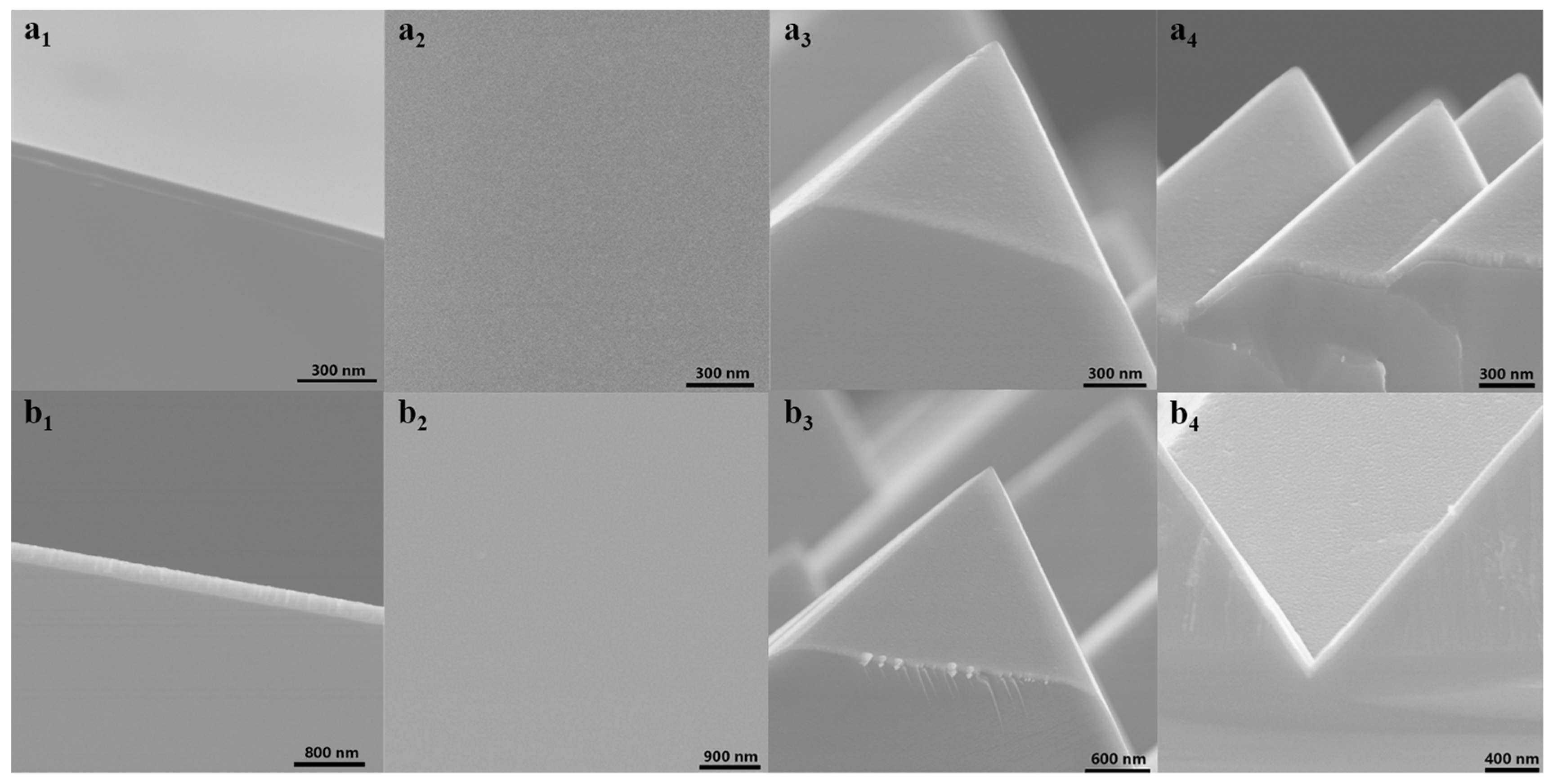
The microscopic morphology of TMO thin films determines the quality of the interface formed with other materials to a great extent. MoOx and WOx films were deposited on polished silicon wafers and random pyramid substrates, respectively, to observe the morphological characteristics of oxide films on different substrates.
Figure 2(a1–a4) are SEM images of MoOx thin film fabricated on different substrates under optimized deposition conditions (hot wire temperature of 1050 °C and oxygen pressure of 0.2 Pa) by HWOSD. For deposition of MoOx on a polished silicon wafer, Figure 2(a1) displays a cross-sectional view of the MoOx film with uniformed thickness. As can be seen from Figure 2(a2), the top view of the MoOx film deposited on the polished silicon wafer exhibited uniform distribution on the surface of the polished silicon wafer. The MoOx films on textured silicon wafers can form a good coverage of the random pyramid light trapping structure, as shown in Figure 2(a3,a4).
WOx (under W wire temperature of 1200 °C and oxygen pressure of 1.0 Pa) were fabricated on different substrates under the optimized preparation process. Figure 2(b1) proved that HWOSD can also achieve uniform growth of tungsten oxide thin films on polished silicon wafers. On the surface of the silicon wafer with random pyramid texture, WOx can also achieve the “conformal” deposition of the light trapping structure, thereby creating the necessary conditions for the subsequent formation of an ideal device interface.
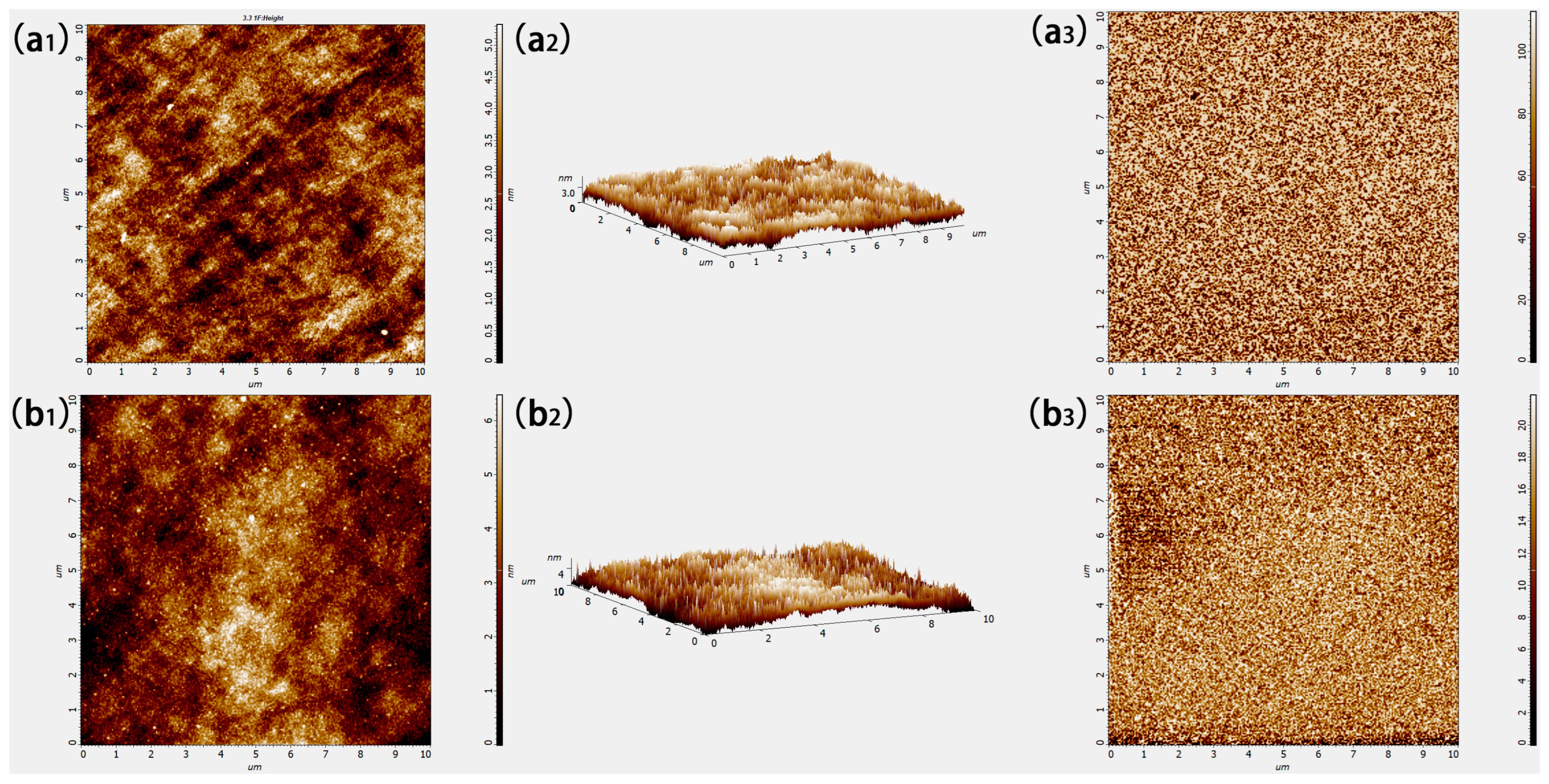
The atomic force microscopy (AFM) was used to characterize the roughness and phase of each film under optimal processing conditions, as shown in Figure 3.
Figure 3(a1,a2) are the 2D and 3D height graphs of the MoOx films deposited on the surface of the polished silicon wafer, respectively. The root mean square roughness (RMS, Sq) in the scanning range of the MoOx film was 1.10 ± 0.02 nm, and the average roughness was 0.88 nm. The phase diagram of MoOx is shown in Figure 3(a3), and the scale on the right is the phase difference between the reflected laser signal of the needle tip and the excitation signal of the needle tip caused by the sample, which represents the sensitivity of different elements in the sample to the tip. The light and dark distributions in the phase diagram in this study respectively represent the distribution of Mo and O elements in the sample, which are evenly distributed in the MoOx film fabricated by HWOSD.
The height diagram of WOx film on the surface of the polished silicon wafer is shown in Figure 3(b1,b2). The RMS roughness Sq of the WOx films was 1.32 ± 0.02 nm, and the average roughness was 1.06 nm. The phase diagram of WOx film (b3) also showed that the WOx film prepared in this study had a uniform phase in Figure 3(b3).
By analyzing the morphological characteristics of transition metal oxides via SEM and AFM, MoOx and WOx thin films deposited by HWOSD possessed uniform thickness and a smooth surface. They could be achieved by “conformal” deposition on the textured surface, which was important to the subsequent application of MoOx and WOx in solar cells.

3.2. Structural Characteristics of TMO Thin Films

The structural characteristics of MoOx and WOx were characterized by X-ray diffraction (XRD), are shown in Figure 4. The X-ray diffractogram of MoOx and WOx films on the glass substrate which be seen that the transition oxide films appeared similar, and no characteristic peaks were presented, indicating an amorphous film, which was related to the relatively low substrate temperature (<200 °C). It is tentatively inferred that the broad, weak humps centred at 2θ ≈ 24.4° (MoOx) and 23.8° (WOx) correspond to the short-range order of Mo-O and W-O polyhedra, respectively, and are in quantitative agreement with the nanometre-scale correlation lengths calculated from the Scherrer equation (~0.8 nm), further supporting the amorphous nature of the films.

3.3. The Electronic Structure of TMO Thin Films

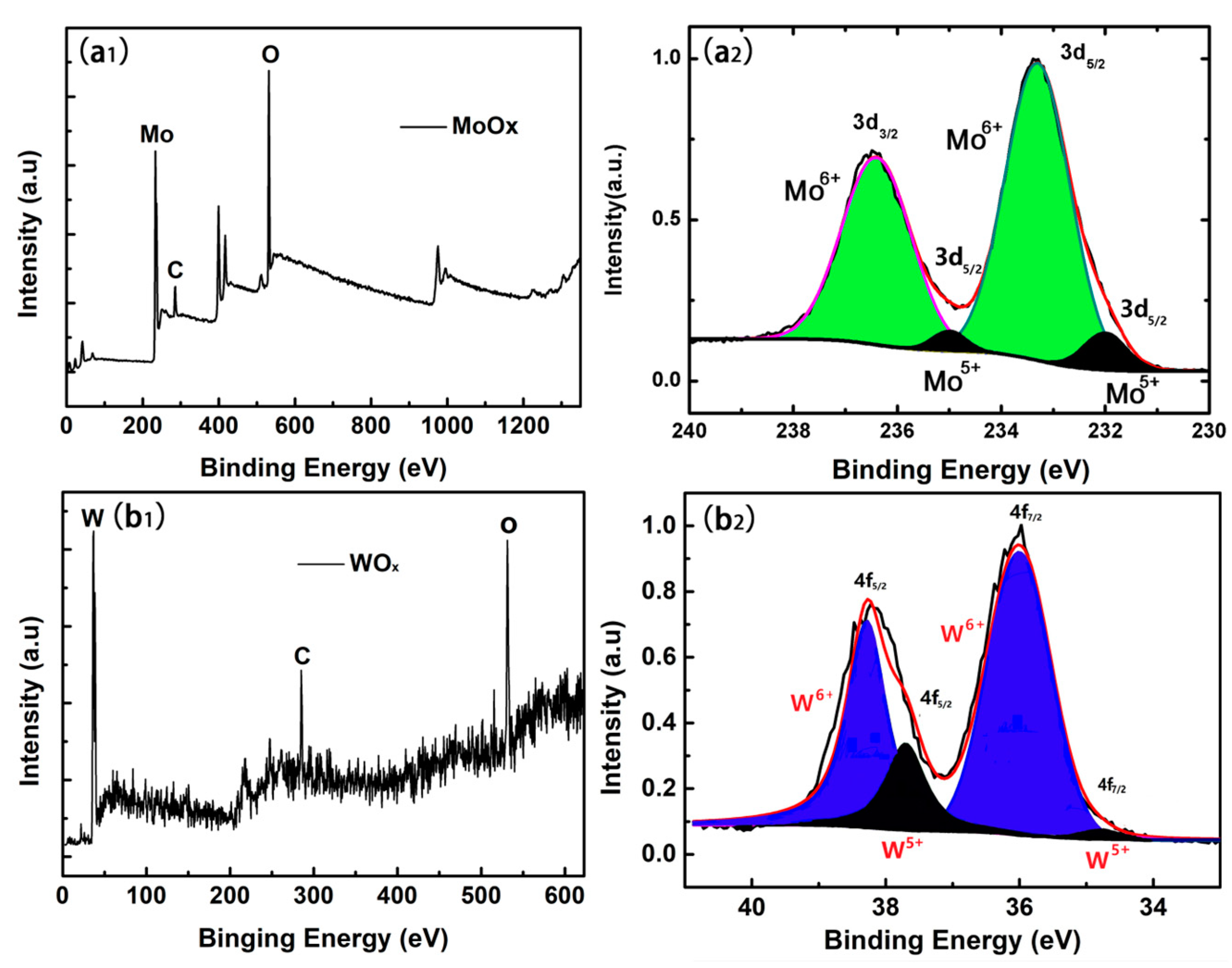
X-ray photoelectron spectroscopy (XPS) was used to analyze the electronic structure characteristics of oxide films. Figure 5(a1,b1) presents the XPS spectra of MoOx and WOx within the entire scanning range, respectively. According to the XPS standards, the approximate position of the element contained in the oxide is found, providing a specific energy interval for the second accurate scan.
The XPS spectrum of the 3d electron of the Mo element in the range of binding energy (BE) of 230 to 240 eV, the molybdenum oxide sample was subjected to a second fine sweep, and the XPS peaking software was used for the obtained data (XPSPEAK-41) can be processed to obtain Figure 5(a2). The positions of the BE at 233.3 and 236.4 eV correspond to the 3d5/2 and 3d3/2 orbital electrons of Mo6+, respectively, and the characteristic peaks at 232 eV and 235 eV originate from the 3d orbital electrons of Mo5+. By fitting and normalizing the characteristic peaks, the content ratio between Mo6+ and Mo5+ (shaded area ratio) in MoOx can be obtained, and the stoichiometric number x in MoOx is estimated to be 2.94 [26]. This value is higher than the result of 2.79–2.86 in MoOx reported in the previous literature, which shows that the higher oxidation state of molybdenum element in MoOx fabricated by HWOSD, implying that the thin film material could have a larger work function.
In the same way, the second fine sweep of the characteristic peak of the W element in WOx thin film material can be obtained as shown in Figure 5(b2). The BE at the positions of 36.0 eV and 38.2 eV corresponds to +6 valence of W ions occupying 4f7/2 and 4f5/2 electron orbitals, respectively. At the positions where the BE are 34.8 eV and 37.0 eV, the +5 valent W ions occupying 4f7/2 and 4f5/2 electron orbitals are presented. Similarly, fitting and normalizing the characteristic peaks resulted in the ratio of 5.33:1 between the W element of +6 and +5 valence in tungsten oxide prepared by this HWOSD. It is inferred that the value of x in WOx is roughly 2.91, which also shows a higher degree of oxidation of tungsten element in the tungsten oxide prepared by the HWOSD method.
The HWOSD-derived MoO2.94 and WO2.91 exhibit elevated M6+/M5+ ratios, evidencing a more highly oxidised, defect-poor surface that favours an increased work function for hole-selective contacts.

3.4. Optical Properties of MoOx and WOx

Figure 6a is a comparison diagram of the transmittance of films of MoOx and WOx with the same thickness (15 nm) fabricated under optimal conditions. It can be seen that TMOs with the same thickness have different light transmittance. The average transmittance of WOx film in the wavelength range of 300–1200 nm is as high as 97.46%, indicating that it has excellent optical performance. Compared to WOx thin films, MoOx films have a bit worse light transmittance with an average transmittance of 94.21%. In general, these two TMOs all have high optical transparency. Their absorption coefficient and optical band gap of each material were analyzed. The absorption coefficient of thin film material α can be expressed as:
α = 1 d l n ( 1 R T )
Where T is the transmittance of the film, d is the thickness of the film, and R is the reflectance of the film material.
The relationship between the light absorption coefficient of the material and the photon energy follows the Tauc law near the absorption edge:
α h ν = β ( h ν E g ) r
where β is a constant; r is an optional parameter, the indirect band gap material is 2, and the direct one is 1/2; Eg is the optical band gap of the material; is the photon energy.
Assuming that the film reflectivity R is 0, and the MoOx and WOx films are amorphous silicon materials, referring to the studies of M. Anwar [33], SH Mohamed [34,35], and S. Sindhu [36], and Kumari et al. [37], and knowing the indirect band gap for the three oxides, our calculate resulted in a Tauc curve, as shown in Figure 6b. Extrapolating the linear portion of the curve to the abscissa, the value corresponding to the intersection point leads to the optical band gap of the material. From Figure 6b, the optical band gaps of MoOx and WOx were 2.67 eV, and 1.86 eV, respectively. M. Anwar and other researchers found that the optical band gap of the MoOx film was affected by the thickness of the film itself [37], the deposition temperature, and the annealing, varying between 2.3 and 2.9, which was similar to that of the MoOx film measured in this work. According to studies by Corsin Battaglia et al. [38,39]. The forbidden band width of the amorphous molybdenum oxide film was 3.0–3.3 eV [40], but the optical band gap of the molybdenum oxide film fabricated in this experiment was 2.61 eV. The random fluctuation of the internal field caused by the disordered structure in the crystalline film, which in turn caused the optical band gap of the amorphous silicon film to change, referring to the studies of Cody, G., D., et al. [41]. It may also be due to the existence of a defect state energy level in the forbidden band of the molybdenum oxide film, which could absorb incident light of a certain wavelength, and the optical band gap was smaller than the forbidden band width [42]. The existence of defect states in the molybdenum oxide film provided a necessary channel for the transport of holes at the interface [43,44]. SH Mohamed and other studies have shown that the optical band gap of WOx films prepared by sputtering increased with the increase of oxygen pressure [35]. When the oxygen pressure increased from 0.01 Pa to 0.52 Pa, the optical band gap of the tungsten oxide prepared also increased from 1.56 eV to 3.18 eV [45]. The fabrication of tungsten oxide in this work had an oxygen pressure of 1.0 Pa, being different from those reported in the literature, which also belonged to a comparable thin film deposition technology under low oxygen pressure. It could be seen from these results that the optical band gap of the oxide was affected by the structural characteristics of the film, the preparation conditions, and the content of elements inside the film.

3.5. Electrical Characteristics of MoOx and WOx

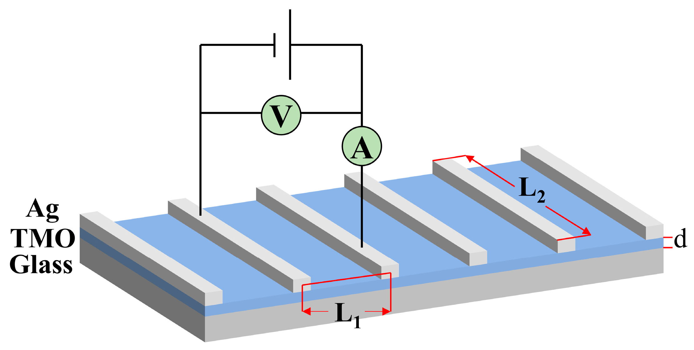
As seen in Figure 7, the HWOSD was used to fabricate a TMO film with a certain thickness on a glass substrate, and a grid electrode was prepared by thermal evaporation on the surface of such films, for testing electrical conductivity. Their conductivity σ (with the unit of S/cm) was obtained by Equation (3), with the corresponding current value when applying the electrical potential between the two electrodes:
σ = I L 1 U d L 2
where d (cm) is the thickness of the film material; U is the voltage (V); I is the current (A); L1 and L2 (cm) are the electrode spacing width and electrode length, as show in Figure 7. The conductivity obtained for MoOx and WOx films were 2.58 × 10⁻⁶ and 5.14 × 10⁻⁷ S/cm, respectively.
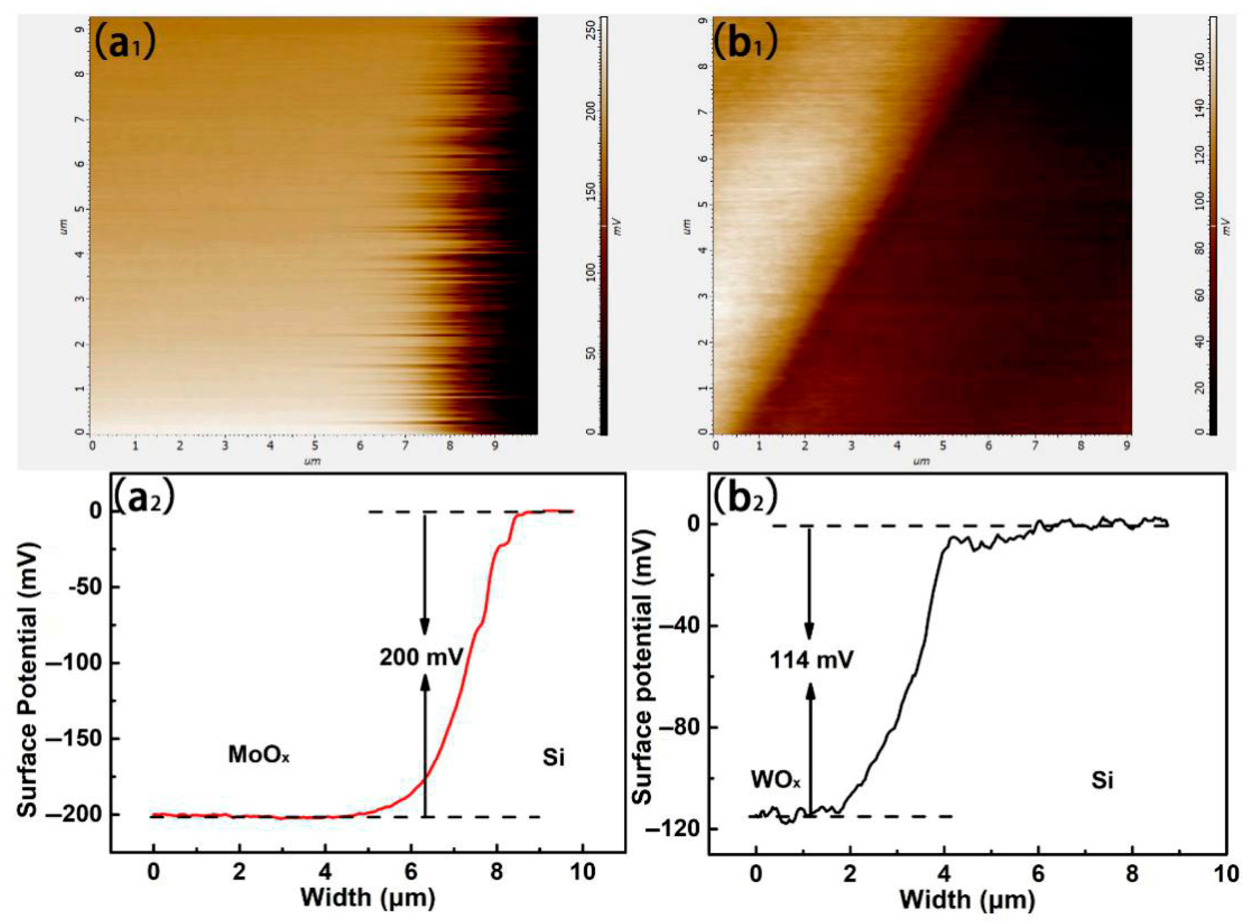
The surface potential of MoOx and WOx on polished silicon wafers was measured by Kelvin Probe Microscopy (KPM), and the energy band relationship at the interface between the transition oxides and the silicon wafer was qualitatively analyzed. The measurement results are shown in Figure 8.
The working principle of the Kelvin probe microscope is: when two different samples are in contact, the Fermi level will be in the same position at the contact interface. But due to the different work functions of the materials, the energy bands are bent at the interface, leading to the redistribution of different charges that generate forces with the probes of the device. It was such tested forces that provided us with the surface potential and the work function of the materials.
Different potential distributions between MoOx and n-Si are illustrated in Figure 8(a1), according to the brightness and darkness of the colors. Figure 8(a2) stands for the potential value on the Z axis obtained from Figure 8(a1). It can be seen that the potential on the MoOx side is about 200 mV lower than that on the Si plate side. It showed that higher work function and lower Fermi level of MoOx than those of n-Si resulted in redistribution of surface charges and therefore the bending of their energy bands at interfaces, building up a potential barrier for electron transport, while benefiting the selective hole transport when they moved towards the MoOx side based on the attraction from MoOx’s low work functions.
The potential distribution of the WOx film in contact with the Si wafer is shown in Figure 8(b1), which follows similar mechanisms to the interactions between MoOx and Si wafers. Figure 8(b2) similarly presents the contact potential difference between WOx and Si in the Z-axis direction. Comparing Figure 8(a2,b2), the contact potential difference of MoOx (200 mV) was found significantly higher than that of WOx (114 mV), which could be inferred that the MoOx film might cause a greater band bending. The different work functions of 6.9 eV for MoOx and 6.5 eV for WOx, respectively, could be the right reason for causing the difference in the bending of the crystalline silicon band.
A direct comparison reveals that MoOx delivers a larger contact-potential difference than WOx, translating into steeper band bending that enhances hole selectivity while suppressing electron recombination.
Figure 9 shows the curve of minority carrier’s lifetime with carrier concentration in n-type CZ silicon wafers with i a-Si:H or MoOx/i a-Si:H composite layers deposited on both sides [26]. Compared with the passivation of amorphous silicon, the symmetric structure of i: a-Si/MoOx (14 nm) covered on both sides of the silicon wafer causes a longer minority lifetime in their injection concentration range of 7 × 1014 cm−3~1 × 1016 cm−3, with 1.3 ms as the highest for MoOx/i a-Si:H/c-Si/i a-Si:H/MoOx can reach. This indicated that MoOx had a strong field passivation effect on silicon wafers; that is, a larger work function of the MoOx film could cause a larger band bending at the contact interface with the Si wafer, thereby reducing the recombination of carriers near the contact. Such results could also be corroborated by the test result of the contact potential of the front surface.
Direct lifetime measurements on MoOx/Si/MoOx stacks were unattainable, indicating a high density of interfacial defect states. Inserting i a-Si:H between MoOx and Si suppresses these defects and simultaneously exploits the strong field-effect passivation of MoOx, yielding a 1.3 ms peak lifetime. Future efforts must therefore focus on defect-state management at the MoOx/Si interface to unlock the full potential of TMO-based contact engineering.

3.6. Effect of Annealing on Optical and Structural Properties of TMO Thin Films

Considering that the TMO films may suffer the temperature changes when being applied to devices and future possible optimizations on their film properties, the effect of annealing temperature on molybdenum oxide (MoOx) and tungsten oxide (WOx) films was studied. The two thin film materials deposited on the glass substrate were rapidly annealed at different temperatures using a fast-annealing apparatus. The morphology, transmittance, and structure of the thin films were studied by means of optical microscope, UV-Vis absorption, and XRD methods.
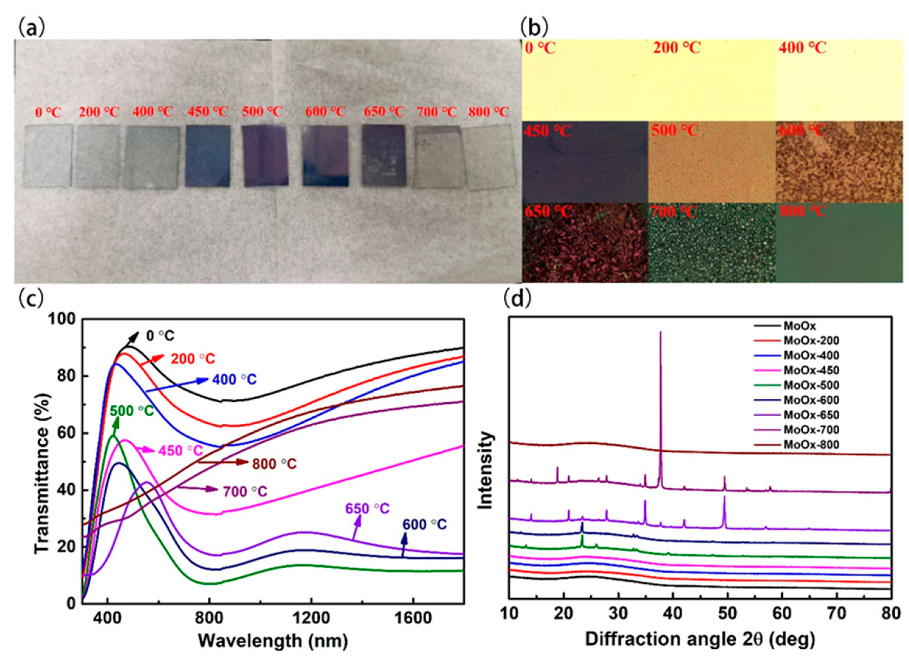
First, under the protection of argon, the molybdenum oxide film was rapidly annealed at 200, 400, 450, 500, 600, 650, 700, and 800 °C, respectively, for 60 s. The morphology, transmittance, and XRD pattern of the films are shown in Figure 10.
As can be seen from Figure 10a,b, when the annealing temperature was less than 400 °C, the appearance of the MoOx film had no obvious changes. As the annealing temperature increased from 450 to 600 °C, the films’ color gradually deepened, and the metallographic microscope showed that the MoOx films gradually appeared granular, implying some structural changes. Further increasing the annealing temperature led to the disappearance of the MoOx film from the substrates. When the annealing temperature reached 800 °C, the granular MoOx had completely disappeared.
Figure 10c shows the transmittance of MoOx at different rapid annealing temperatures. With the annealing temperature increased, the transmittance of the MoOx film as a whole decreased firstly and then increased. When the annealing temperature was raised from 200 to 500 °C, the transmittance of the film dropped to a minimum; a possible reason was that the structure change of the molybdenum oxide film affected its transmittance to some extent. When the rapid-annealing temperature continued to rise, the film’s transmission rate rose continuously because the higher annealing temperature might cause the decomposition or sublimation of MoOx film, exposing the glass substrate, thereby increasing the transmission rate.
From the XRD pattern of Figure 10d, it can be seen that when the annealing temperature was <450 °C, the structure of the MoOx film remained unchanged, still being amorphous. When the rapid-annealing temperature rose to 500 °C, the XRD pattern of MoOx presented diffraction peaks at 13.04°, 23.38°, 25.94°, 39.13°, 47.35°, 52.77°, 39.13°, 47.23°, 52.76°, respectively, corresponding to crystal planes of (0 0 1), (1 0 0), (0 0 2), (0 0 3), (2 0 0), (1 0 −4), and (2 1 0) for MoO3 monoclinic phase. When the annealing temperature was 600 °C, the disappearance of characteristic diffraction peaks at 13.04°, 25.94°, 39.13°revealed the vanishing of (0 0 1), (0 0 2), and (0 0 3) crystal planes. When increasing the annealing temperature to 650 °C, the characteristic peak at 23.38° was found much less pronounced, and the one characteristic peak at 32.65° disappeared, meanwhile generation of new diffraction peaks at 13.88°, 20.88°, 27.88° suggested newly formed (6 4 0), (10 4 0), and (6 6 1) crystal planes of MoO2.8. And the ones at 34.89°, 37.69° proved the presence of (1 −2 7) (3 −2 4) crystal planes of Mo9O26, while the one at 57.01° stood for the (14 1 1) crystal plane of Mo4O11. Continued to increase the temperature to 700 °C, the crystal plane of (3 −2 4) for Mo9O26 claimed the preferred crystal orientation, corresponding to a peak at 37.66°, accompanied by a peak at 18.74° exhibiting (−4 0 1) crystal plane of Mo4O11. In summary, as the annealing temperature rose, the amorphous MoOx film generated monoclinic MoO3 crystals at 500 and 600 °C. As the temperature continued to rise to 650 and 700 °C, MoO2.8, Mo9O26, and Mo4O11 appeared; it could be seen that the oxygen element in the MoOx film had a tendency to detach from the film. Literature showed that the reduction of X in MoOx might cause a decrease in the work function of the MoOx film. When it continues to increase to 800 °C, the MoOx thin film in the glass has completely decomposed and escaped the glass substrate, as shown in Figure 10a.
As reported in the literature, an appropriate amount of oxygen was in need to be to maintain a higher work function of the MoOx film by thermal evaporation technique using MoOx powders as the source, which could be attributed to the desorption of oxygen element from MoOx at high temperature [46].
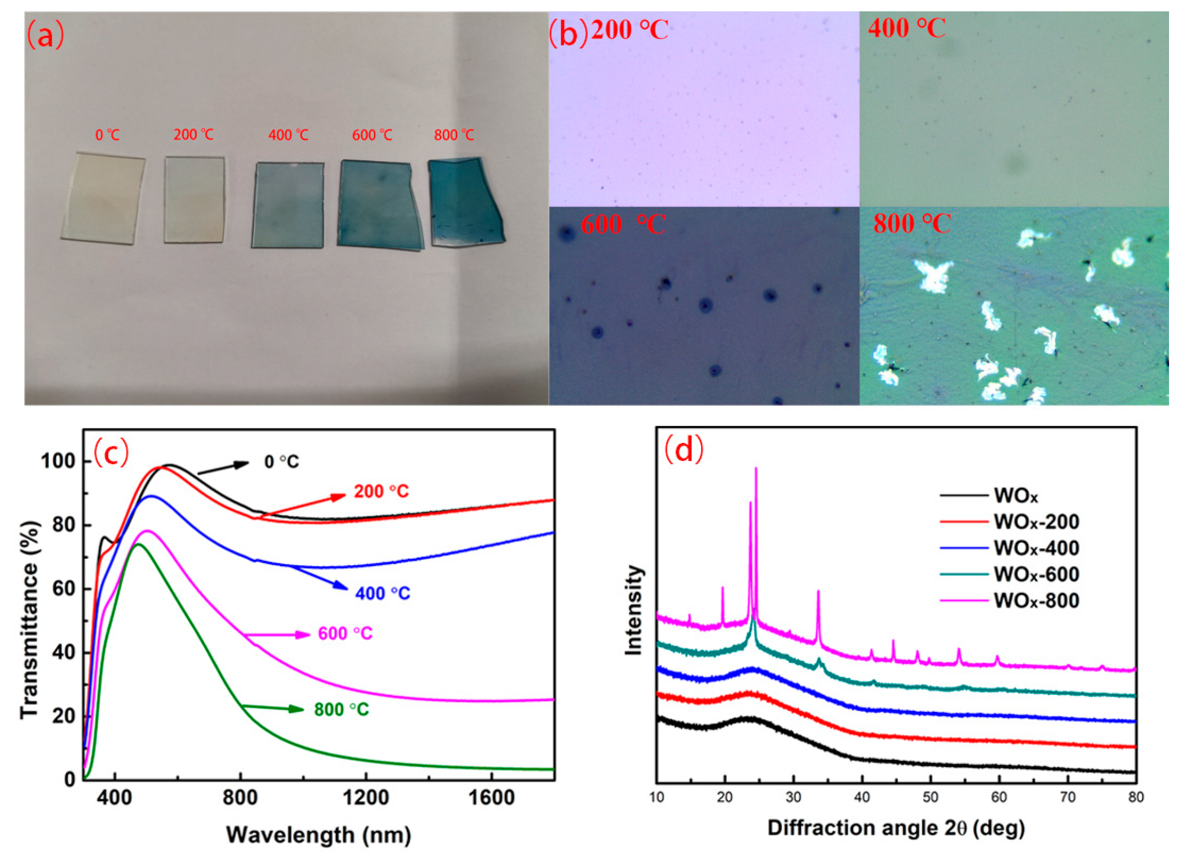
Using the same method and process, the rapid annealing performance of WOx film was studied, as shown in Figure 11. It was seen from Figure 11a that rapid annealing gradually changed the color of the WOx film from light to dark. Figure 11b confirmed agglomeration phenomenon at some positions of the WOx film as the annealing temperature gradually rose up to 600 °C. When the annealing temperature was further increased to 800 °C, the WOx film had partially peeled off. The position of the film was seen as a “wrinkle”, suggesting a stress change inside the film.
Figure 11c shows the effect of different annealing temperatures on the transmittance of the WOx films. As the rapid-annealing temperature increased, the transmittance of the WOx film gradually decreased, implying that it might cause structural changes in the WOx film. As can be seen from Figure 11d, when the temperature lay between 200 and 400 °C, the WOx film still maintained an amorphous state. When the rapid- annealing temperature was rose to 600 °C, peaks of diffraction at 23.96°, 34.08°, 42.11°, 49.04°, 55.25°, and 61.07°, respectively, corresponding to (1 0 0), (1 1 0), (1 1 1), (2 1 0), (2 1 0), and (2 1 1) crystal planes. Continued to raise the annealing temperature to 800 °C, the characteristic peaks at 23.72°, 33.60°, 41.32°, 44.68°, 48.03°, 54.15°, 59.75°, and 70.04°, were recognized as crystal planes of (1 1 0), (2 0 0), (2 0 1), (2 1 1), (2 2 0), (3 1 0), (3 1 1), and (4 0 0) for WO2.9. When the annealing temperature reached 800 °C, the phenomenon of X reduction in WOx was also found.
In a word, HWOSD-grown MoOx and WOx films exhibit markedly different thermal-stability behaviors. MoOx remains amorphous below 450 °C, crystallises into monoclinic MoO3 at 500 °C, and then follows a progressive reduction sequence-MoO3-MoO2.8-Mo9O26 -Mo4O11, until complete sublimation at 800 °C. This trajectory is driven by the intrinsically lower melting/boiling points and higher oxygen volatility of molybdenum oxides. The accompanying optical signature is a transient drop in transmittance during crystallization, followed by a sharp rise as the film disappears. WOx, in contrast, retains an amorphous structure up to 400 °C and crystallises into WO3 at 600 °C. Continued heating to 800 °C produces only a slight reduction to WO2.9, accompanied by densification and partial peel-off rather than catastrophic loss. Consequently, WOx offers a 200–300 °C wider thermal window than MoOx. The difference translates directly to interface stability: MoOx’s steeper band bending (200 mV contact-potential difference) and higher work function provide superior hole selectivity at low temperature, whereas WOx’s 114 mV offset and work function remain stable above 600 °C. Thus, MoOx serves as an optimal low-temperature hole-selective layer, while WOx is the material of choice for devices subjected to prolonged high-temperature processing.

3.7. The Performance of Heterojunction Cells with MoOx and WOx as HTLs

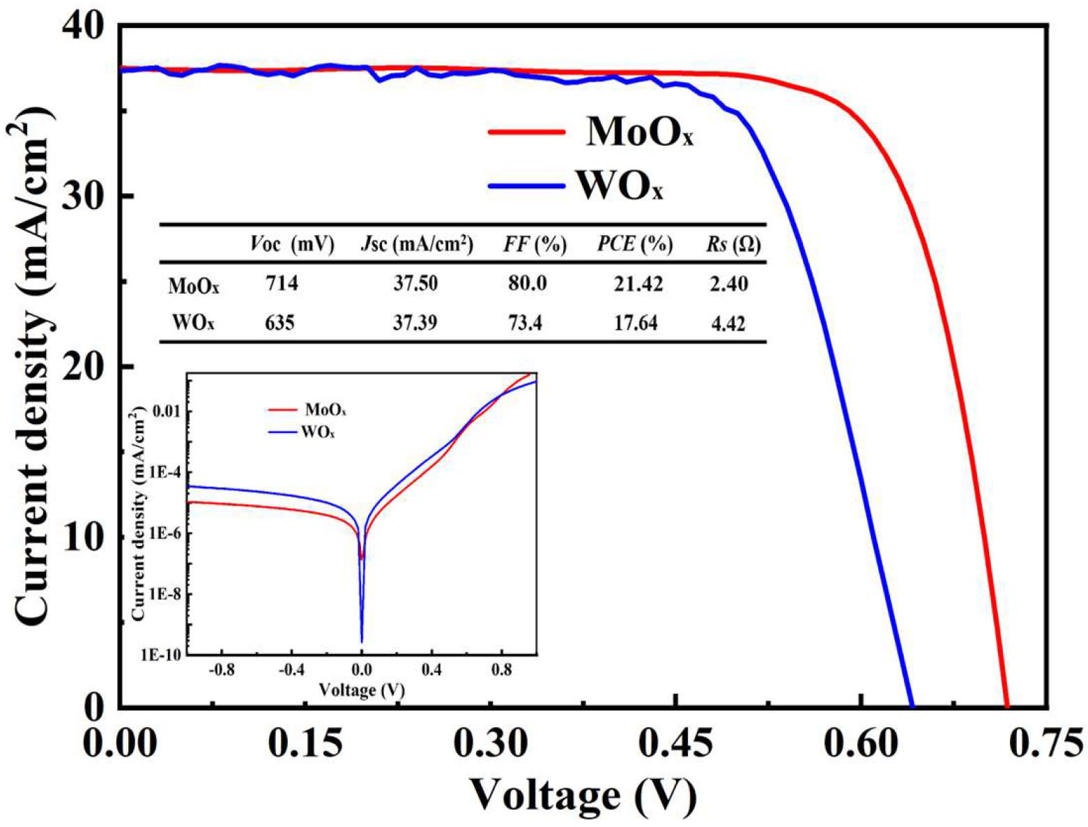
To investigate the performance of transition metal oxide thin films prepared by HWOSD in device applications, heterojunction solar cells were fabricated using MoOx and WOx as hole transport layers (HTLs), and their device performance was evaluated, as depicted in Figure 12.
Based on the observations and experimental results, both types of solar cells exhibit relatively excellent performance. However, the SHJ solar cell employing MoOx as the hole transport layer (HTL) outperforms those utilizing WOx as HTLs. The VOC of heterojunction solar cells with WOx as HTLs was lower than that of MoOx solar cells. The factors that affected VOC mainly included the work function of TMO and interface characteristics. It is generally believed that the higher the TMO work function, the greater the bending degree of the energy band, which finding is consistent with the results of the Kelvin probe microscope. It can be seen from the reverse saturation current density was MoOx < WOx, which could exhibit the density of interface defect states to a certain extent.
The FF of the device is mainly affected by the series resistance. The Rs of MoOx solar cells solar cell was the smallest, which was 2.40 Ω, followed by 4.42 Ω for WOx solar cells, respectively. Considering that the conductivity of the TMO material exerts a substantial impact on the Rs of these devices, the results of the FF and Rs provide compelling validation for the measured electrical conductivity of MoOx and WOx films.
The MoOx-equipped cell delivers Voc = 714 mV, FF = 80% and Rs = 2.40 Ω, outperforming the WOx cell (Voc = 635 mV, FF = 73.4%, Rs = 4.42 Ω). The 79 mV Voc gain stems from MoOx’s higher work function, which induces steeper band bending and lowers reverse saturation current (J0, MoOx < J0, WOx). The lower Rs reflects superior TMO conductivity. These results confirm that interface passivation and defect-state control remain the primary levers for further device optimisation.

4. Conclusions

In this work, HWOSD enabled the reproducible deposition of MoOx and WOx thin films, and conducted a systematic, side-by-side evaluation of their structural, optical, and electronic properties. Characterization techniques such as SEM, AFM, and XRD revealed that the oxide films exhibit smooth surfaces, uniform thickness, and excellent conformal coverage over textured substrates. XPS analysis indicated that the oxygen-to-metal ratios in MoOx and WOx films were 2.94 and 2.91, respectively. Both oxide films demonstrated good optical transmittance, with optical bandgaps of 2.67 eV for MoOx and 1.86 eV for WOx. Electrical property evaluations showed that the films possess favorable conductive characteristics and good contact potential differences with silicon wafers. Heterojunction solar cells employing these oxide films as hole-selective transport layers exhibited promising performance parameters. The results suggest that the TMO thin films prepared by the HWOSD method possess excellent electronic properties and hold great potential for broader applications in the fabrication of photocatalysis, flexible optoelectronics, and roll-to-roll manufacturing. Nevertheless, their long-term thermal stability awaits rigorous validation, while precise doping for oxygen-vacancy control and advanced interface engineering remain pivotal for future optimization.

Author Contributions

Conceptualization, F.L., T.L. (Ting Liang) and C.L.; Methodology, F.L., T.L. (Ting Liang) and C.L.; Formal analysis, F.L., T.L. (Tengteng Li) and H.Q.; Investigation, F.L.; Data curation, F.L. and H.Q.; Writing—original draft, F.L. and Q.K.; Writing—review & editing, F.L., J.Y. and C.L.; Visualization, F.L. and Z.K.; Supervision, T.L. (Ting Liang) and C.L.; Project administration, F.L. and C.L.; Funding acquisition, F.L., T.L. (Tengteng Li) and J.Y. All authors have read and agreed to the published version of the manuscript.

Funding

This work was supported by the National Natural Science Foundation of China (No. 62304209 and 62301509), the Key Research and Development Program of Shanxi Province (No. 202402060301004 and 202302030201001), and the Fundamental Research Program of Shanxi Province (No. 20210302123203, 202203021222079, and 202103021223185).

Data Availability Statement

The original contributions presented in this study are included in the article. Further inquiries can be directed to the corresponding authors.

Conflicts of Interest

The authors declare no conflicts of interest.

References

  1. Chen, Z.; Liu, Y.; Zhang, H.; Liu, Z.; Tian, H.; Sun, Y.; Meng, Z.; Yi, Z.; Sun, J.; Xie, Y. Electric field control of superconductivity at the LaAlO3/KTaO3(111) interface. Science 2021, 372, 721–724. [Google Scholar] [CrossRef]
  2. Han, Y.; Lao, B.; Zheng, X.; Li, S.; Li, R.-W.; Wang, Z. Transition metal oxides: A new frontier in spintronics driven by novel quantum states and efficient charge-spin interconversion. Front. Mater. 2024, 11, 1444769. [Google Scholar] [CrossRef]
  3. Peng, Y.; Tian, H.; Yao, M.; Li, X.; Tang, X.; Jiao, J.; Zhu, Q.; Cao, J. First-principles prediction of high carrier mobility for β-phase MX2N4 (M = Mo, W, X = Si, Ge) monolayers. Sci. Rep. 2024, 14, 22548. [Google Scholar] [CrossRef]
  4. Park, K.-W.; Kolpak, A.M. Optimal methodology for explicit solvation prediction of band edges of transition metal oxide photocatalysts. Commun. Chem. 2019, 2, 79. [Google Scholar] [CrossRef]
  5. Vijayan, A.; Sandhyarani, N. Efficient and sustainable hydrogen evolution reaction: Enhanced photoelectrochemical performance of ReO3-incorporated Cu2Te catalysts. Energy Adv. 2024, 3, 1092–1098. [Google Scholar] [CrossRef]
  6. Jia, H.; Meng, L.; Lu, Y.; Liang, T.; Yuan, Y.; Hu, Y.; Dong, Z.; Zhou, Y.; Guan, P.; Zhou, L.; et al. Boosting the efficiency of electrocatalytic water splitting via in situ grown transition metal sulfides: A review. J. Mater. Chem. A 2024, 12, 28595–28617. [Google Scholar] [CrossRef]
  7. Li, M.; Lin, W.; Ji, Y.; Guan, L.; Qiu, L.; Chen, Y.; Lu, Q.; Ding, X. Recent progress in high-voltage P2-NaxTMO2 materials and their future perspectives. RSC Adv. 2024, 14, 24797–24814. [Google Scholar] [CrossRef]
  8. Tao, S.; Wang, J.; Zhang, J. Conductive Metal–Organic Frameworks and Their Electrocatalysis Applications. ACS Nano 2025, 19, 9484–9512. [Google Scholar] [CrossRef]
  9. Li, W.; Zhao, X.; Bi, Q.; Ma, Q.; Han, L.; Tao, K. Recent advances in metal–organic framework-based electrode materials for supercapacitors. Dalton Trans. 2021, 50, 11701–11710. [Google Scholar] [CrossRef]
  10. Long, Z.; Kelly, H.R.; Videla, P.E.; Menzel, J.P.; Lian, T.; Kubiak, C.P.; Batista, V.S. Control of Reversible Oxidative Addition/Reductive Elimination of Surface-Attached Catalysts by External Electric Fields. J. Phys. Chem. Lett. 2025, 16, 2881–2886. [Google Scholar] [CrossRef]
  11. Lv, Q.; Chi, K.; Zhang, Y.; Xiao, F.; Xiao, J.; Wang, S.; Loh, K.P. Ultrafast charge/discharge solid-state thin-film supercapacitors via regulating the microstructure of transition-metal-oxide. J. Mater. Chem. A 2017, 5, 2759–2767. [Google Scholar] [CrossRef]
  12. Irfan, S.; Haleem, Y.A.; Irshad, M.I.; Saleem, M.F.; Arshad, M.; Habib, M. Tunability of the Optical Properties of Transition-Metal-Based Structural Phase Change Materials. Optics 2023, 4, 351–363. [Google Scholar] [CrossRef]
  13. Wojtasik, K.; Wojtasik, M.; Suchanek, K.; Zięba, M.; Karasiński, P.; Pakieła, W.; Żak, G.; Krasodomski, W. Effect of pyrolytic carbon addition on the structural and optical properties of TiO2 composite thin films. Sci. Rep. 2025, 15, 8078. [Google Scholar] [CrossRef]
  14. Jung, Y.-C.; Yu, Y.-J.; Kim, Y.-K.; Lee, J.H.; Seo, J.H.; Choi, J.-Y. Asymmetric TMO-Metal-TMO Structure for Enhanced Efficiency and Long-Term Stability of Si-Based Heterojunction Solar Cells. Materials 2023, 16, 5550. [Google Scholar] [CrossRef] [PubMed]
  15. Fatheema, J.; Shahid, T.; Mohammad, M.A.; Islam, A.; Malik, F.; Akinwande, D.; Rizwan, S. A comprehensive investigation of MoO3 based resistive random access memory. RSC Adv. 2020, 10, 19337–19345. [Google Scholar] [CrossRef]
  16. Kamoun, O.; Boukhachem, A.; Amlouk, M.; Ammar, S. Physical study of Eu doped MoO3 thin films. J. Alloys Compd. 2016, 687, 595–603. [Google Scholar] [CrossRef]
  17. Car, T.; Jakovac, I.; Šarić, I.; Bernstorff, S.; Micetic, M. Structural, Optical and Electrical Properties of Al+MoO3 and Au+MoO3 Thin Films Prepared by Magnetron Co-deposition. Materials 2021, 14, 766. [Google Scholar] [CrossRef]
  18. Muslu, E.; Eren, E.; Oksuz, A.U. Research progress on flexible WO3 based thin film electrodes for supercapacitor applications: A comprehensive review. Emergent Mater. 2024, 7, 2205–2236. [Google Scholar] [CrossRef]
  19. Yao, Y.; Sang, D.; Zou, L.; Wang, Q.; Liu, C. A Review on the Properties and Applications of WO3 Nanostructure—Based Optical and Electronic Devices. Nanomaterials 2021, 11, 2136. [Google Scholar] [CrossRef]
  20. Morankar, P.J.; Amate, R.U.; Bhosale, M.K.; Jeon, C.-W. PVP-Engineered WO3/TiO2 Heterostructures for High-Performance Electrochromic Applications with Enhanced Optical Modulation and Stability. Polymers 2025, 17, 1683. [Google Scholar] [CrossRef]
  21. Yang, X.; Zhao, S.; Huang, Q.; Yu, C.; Zhou, J.; Liu, X.; Su, X.; Zhao, Y.; Hou, G. Sub-stochiometric MoOx by radio-frequency magnetron sputtering as hole-selective passivating contacts for silicon heterojunction solar cells. Chin. Phys. B 2022, 31, 098401. [Google Scholar] [CrossRef]
  22. Borgschulte, A.; Sambalova, O.; Delmelle, R.; Jenatsch, S.; Hany, R.; Nüesch, F. Hydrogen reduction of molybdenum oxide at room temperature. Sci. Rep. 2017, 7, 40761. [Google Scholar] [CrossRef] [PubMed]
  23. Rizzuto, C.; Barberi, R.C.; Castriota, M. Tungsten and Titanium Oxide Thin Films Obtained by the Sol-Gel Process as Electrodes in Electrochromic Devices. Front. Mater. 2022, 9, 912013. [Google Scholar] [CrossRef]
  24. Wang, Z.; Liu, Z.; Lin, H.; Ye, F.; Gao, P. Hot wire Oxidatione Sublimation derived work function tunable WOx thin films for building hole-selective contacts. Mater. Today Energy 2023, 38, 101439. [Google Scholar] [CrossRef]
  25. Guo, C.; Li, J.; Liu, R.; Zhang, D.; Qiu, J.; Zhuang, Z.; Chen, Y.; Qiu, Q.; Liu, W.; Huang, Y.; et al. In-situ deposition of tungsten oxide hole-contact by Hot-Wire CVD and its application in dopant-free heterojunction solar cells. Semicond. Sci. Technol. 2023, 38, 015007. [Google Scholar] [CrossRef]
  26. Li, F.; Zhou, Y.; Yang, Y.; Dong, G.; Zhou, Y.; Liu, F.; Yu, D. Silicon Heterojunction Solar Cells with MoOx Hole-Selective Layer by Hot Wire Oxidation–Sublimation Deposition. Sol. RRL 2020, 4, 1900514. [Google Scholar] [CrossRef]
  27. Tan, G.-L.; Tang, D.; Dastan, D.; Jafar, A.; Shi, Z.C.; Chu, Q.-Q.; Silva, J.P.B.; Yin, X.-T. Structures, morphological control, and antibacterial performance of tungsten oxide thin films. Ceram. Int. 2021, 47, 17153–17160. [Google Scholar] [CrossRef]
  28. Mehmood, H.; Bektaş, G.; Yildiz, İ.; Tauqeer, T.; Nasser, H.; Turan, R. Electrical, optical and surface characterization of reactive RF magnetron sputtered molybdenum oxide films for solar cell applications. Mater. Sci. Semicond. Process. 2019, 101, 46–56. [Google Scholar] [CrossRef]
  29. Khanlary, M.R.; Rahmani, E.; Pasalari, Z.; Reyhani, A. Post-annealing effect on the structural and optical properties of tungsten trioxide thin films prepared by thermal evaporation. Mater. Chem. Phys. 2025, 338, 130670. [Google Scholar] [CrossRef]
  30. Al-Muntaser, A.A.; Nasher, M.A.; Makhlouf, M.M. Structural, electrical, and linear/nonlinear optical characteristics of thermally evaporated molybdenum oxide thin films. Ceram. Int. 2022, 48, 8069–8080. [Google Scholar] [CrossRef]
  31. Krishna Prasad, A.; Kim, J.-Y.; Kang, S.-H.; Ahn, K.-S. Molybdenum induced defective WO3 multifunctional nanostructure as an electrochromic energy storage device: Novel assembled photovoltaic-electrochromic Mo–WO3 film. J. Ind. Eng. Chem. 2024, 135, 388–396. [Google Scholar] [CrossRef]
  32. Fu, Q.; Chen, J.; Shi, C.; Ma, D. Room-Temperature Sol–Gel Derived Molybdenum Oxide Thin Films for Efficient and Stable Solution-Processed Organic Light-Emitting Diodes. ACS Appl. Mater. Interfaces 2013, 5, 6024–6029. [Google Scholar] [CrossRef]
  33. Anwar, M.; Hogarth, C.A. Optical properties of amorphous thin films of MoO3 deposited by vacuum evaporation. Phys. Status solidi (a) 1988, 109, 469–478. [Google Scholar] [CrossRef]
  34. Mohamed, S.H.; Anders, A. Structural, optical and electrical properties of WOxNy films deposited by reactive dual magnetron sputtering. Surf. Coat. Technol. 2006, 201, 2977–2983. [Google Scholar] [CrossRef]
  35. Mohamed, S.; Mohamed, H.; El Ghani, H.A. Development of structural and optical properties of WOx films upon increasing oxygen partial pressure during reactive sputtering. Phys. B Condens. Matter 2011, 406, 831–835. [Google Scholar] [CrossRef]
  36. Sindhu, S.; Sanghi, S.; Agarwal, A.; Seth, V.P.; Kishore, N. Structural, optical, physical and electrical properties of V2O5.SrO.B2O3 glasses. Spectrochim. Acta Part A Mol. Biomol. Spectrosc. 2006, 64, 196–204. [Google Scholar] [CrossRef] [PubMed]
  37. Kumari, S.; Singh, K.; Singh, P.; Kumar, P.; Thakur, A. Thickness dependent structural, morphological and optical properties of molybdenum oxide thin films. SN Appl. Sci. 2020, 2, 1439. [Google Scholar] [CrossRef]
  38. Battaglia, C.; Yin, X.; Zheng, M.; Sharp, I.D.; Chen, T.; McDonnell, S.; Azcatl, A.; Carraro, C.; Ma, B.; Maboudian, R.; et al. Hole Selective MoOx Contact for Silicon Solar Cells. Nano Lett. 2014, 14, 967–971. [Google Scholar] [CrossRef] [PubMed]
  39. Battaglia, C.; de Nicolás, S.M.; De Wolf, S.; Yin, X.; Zheng, M.; Ballif, C.; Javey, A. Silicon heterojunction solar cell with passivated hole selective MoOx contact. Appl. Phys. Lett. 2014, 104, 113902. [Google Scholar] [CrossRef]
  40. Borah, D.J.; Mostako, A.; Saikia, P.; Dutta, P. Effect of thickness and post deposition annealing temperature on the structural and optical properties of thermally evaporated molybdenum oxide films. Mater. Sci. Semicond. Process. 2019, 93, 111–122. [Google Scholar] [CrossRef]
  41. Cody, G.D.; Tiedje, T.; Abeles, B.; Moustakas, T.D.; Brooks, B.; Goldstein, Y. Disorder and the Optical Absorption Edge of Hydrogenated Amorphous Silicon. Phys. Rev. Lett. 1981, 42, C4-301. [Google Scholar]
  42. Al-Kuhaili, M.F.; Mekki, M.B. Laser-induced photocoloration in molybdenum oxide thin films. J. Alloys Compd. 2021, 885, 161043. [Google Scholar] [CrossRef]
  43. García-Hernansanz, R.; García-Hemme, E.; Montero, D.; Olea, J.; del Prado, A.; Mártil, I.; Voz, C.; Gerling, L.G.; Puigdollers, J.; Alcubilla, R. Transport mechanisms in silicon heterojunction solar cells with molybdenum oxide as a hole transport layer. Sol. Energy Mater. Sol. Cells 2018, 185, 61–65. [Google Scholar] [CrossRef]
  44. Mahato, S.; Voz, C.; Biswas, D.; Bhunia, S.; Puigdollers, J. Defect states assisted charge conduction in Au/MoO3–x/n-Si Schottky barrier diode. Mater. Res. Express 2019, 6, 036303. [Google Scholar] [CrossRef]
  45. Mahjabin, S.; Haque, M.M.; Sobayel, K.; Selvanathan, V.; Jamal, M.S.; Bashar, M.S.; Sultana, M.; Hossain, M.I.; Shahiduzzaman, M.; Algethami, M.; et al. Investigation of Morphological, Optical, and Dielectric Properties of RF Sputtered WOx Thin Films for Optoelectronic Applications. Nanomaterials 2022, 12, 3467. [Google Scholar] [CrossRef] [PubMed]
  46. Pan, T.; Li, J.; Lin, Y.; Xue, Z.; Di, Z.; Yin, M.; Wang, J.; Lu, L.; Yang, L.; Li, D. Structural and optical studies of molybdenum oxides thin films obtained by thermal evaporation and atomic layer deposition methods for photovoltaic application. J. Mater. Sci. Mater. Electron. 2021, 32, 3475–3486. [Google Scholar] [CrossRef]
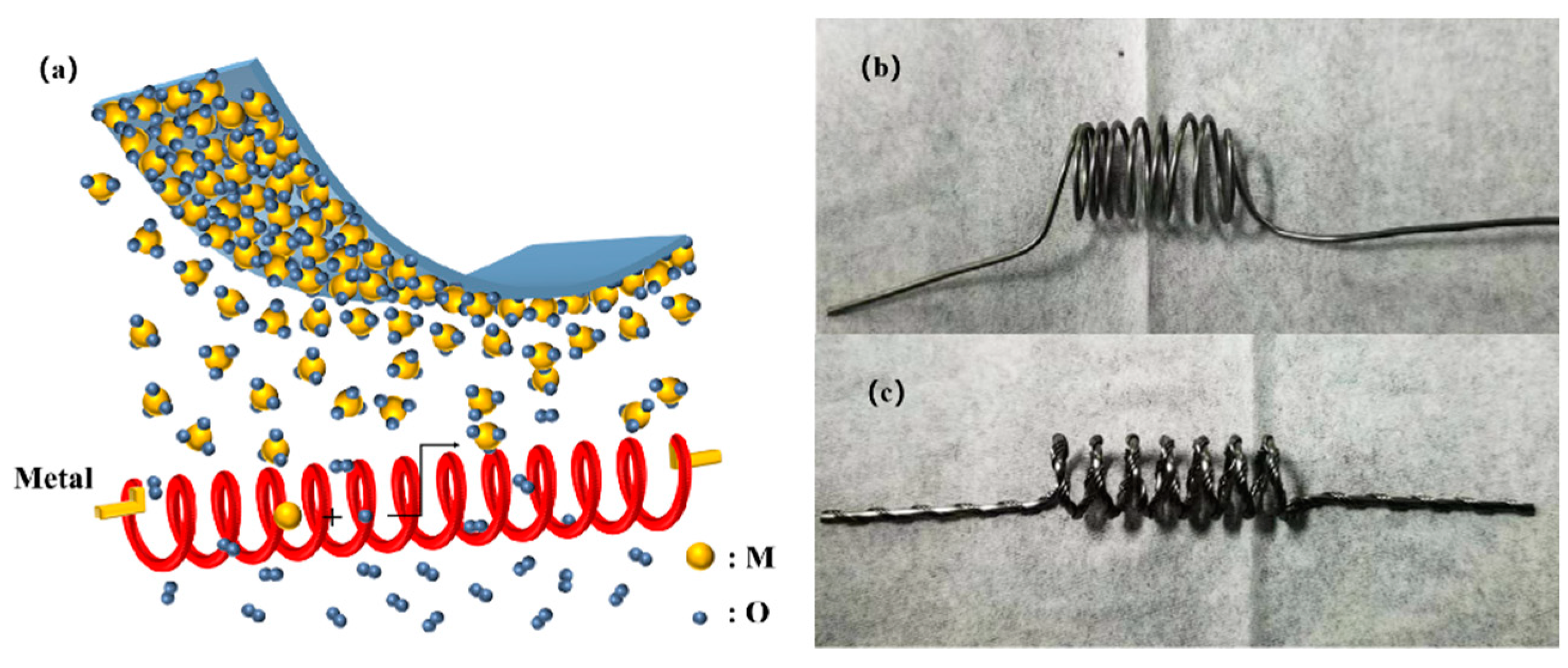
Figure 1. (a) Schematic diagram of hot-wire oxidation sublimation deposition method, (b) Molybdenum wire (99.9%, diameter d = 1.0 mm), (c) Tungsten wire (99.7%, Two tungsten wires with diameter d = 1.0 mm are intertwined).
Materials 18 04083 g001
Figure 2. SEM images of molybdenum oxide (a1a4), tungsten oxide (b1b4) on different substrates: 1 & 2, cross-sectional and top-view on a polished silicon wafer; 3 & 4 on textured silicon wafers.
Materials 18 04083 g002
Figure 3. AFM height (a1,b1), 3D height (a2,b2) and phase (a3,b3) images of MoOx (a1a3) and WOx (b1b3) films.
Materials 18 04083 g003
Figure 4. X-ray diffractogram of transition metal oxides (MoOx and WOx).
Materials 18 04083 g004
Figure 5. X-ray photoelectron spectroscopy (XPS) of MoOx (a1) and WOx (b1), and spectra for: Mo 3d core level in MoOx films (a2), W 4f core level for WOx films (b2).
Materials 18 04083 g005
Figure 6. The transmittance (a) and optical band gap (b) of TMOs.
Materials 18 04083 g006
Figure 7. Schematic diagram of transition metal oxide conductivity measurement.
Materials 18 04083 g007
Figure 8. (a1) Potential distribution of MoOx film on silicon wafer surface. (a2) The surface potential difference between MoOx and silicon in the z-axis direction. (b1) The potential distribution of WOx film on silicon wafer surface. (b2) The surface potential difference between WOx and silicon in the z-axis direction.
Materials 18 04083 g008
Figure 9. Measured effective lifetimes for samples with the structures of i a-Si:H/c-Si/i a-Si:H and MoOx/i a-Si:H/c-Si/i a-Si:H/MoOx as a function of excess carrier density in the range of 7 × 1014 cm−3 ~ 1 × 1016 cm−3.
Materials 18 04083 g009
Figure 10. Photos (a), optical images (b), transmittance (c), and XRD diffractograms (d) of MoOx films at different rapid-annealing temperatures.
Materials 18 04083 g010
Figure 11. Photos (a), morphology under optical microscope (b), transmittance (c), and XRD pattern (d) of WOx films at different rapid annealing temperatures.
Materials 18 04083 g011
Figure 12. The light and dark J-V curves of the heterojunction solar cells with MoOx and WOx as HTLs.
Materials 18 04083 g012
Disclaimer/Publisher’s Note: The statements, opinions and data contained in all publications are solely those of the individual author(s) and contributor(s) and not of MDPI and/or the editor(s). MDPI and/or the editor(s) disclaim responsibility for any injury to people or property resulting from any ideas, methods, instructions or products referred to in the content.