
Investigation of Current Effect of Suspended Graphene Pressure Sensor


Highlights
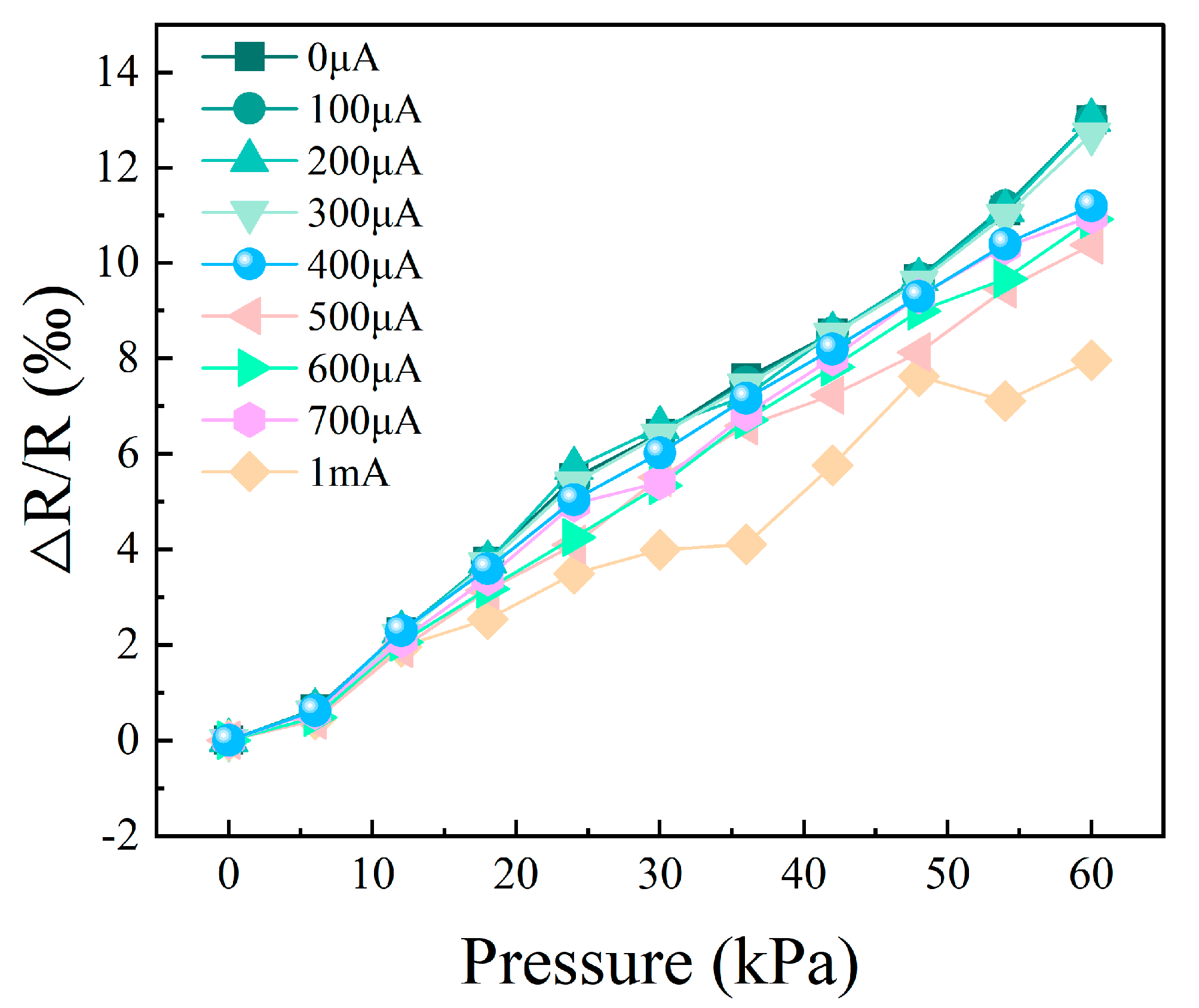
- Graphene sensor shows <5% error (0–60 kPa), proving stability.
- Resistance first rises then falls (>700 μA) due to O2 adsorption/desorption.
- Piezoresistance degrades beyond 300 μA, reducing stability
Abstract
1. Introduction
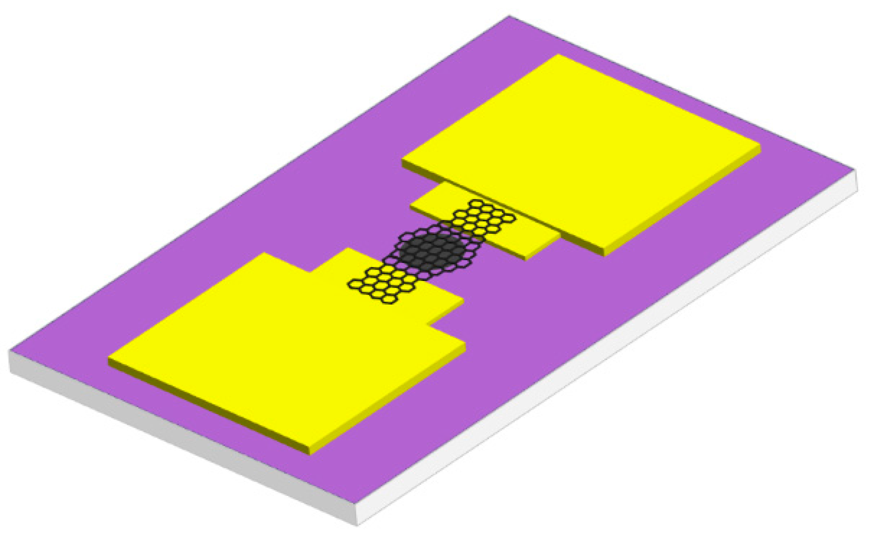
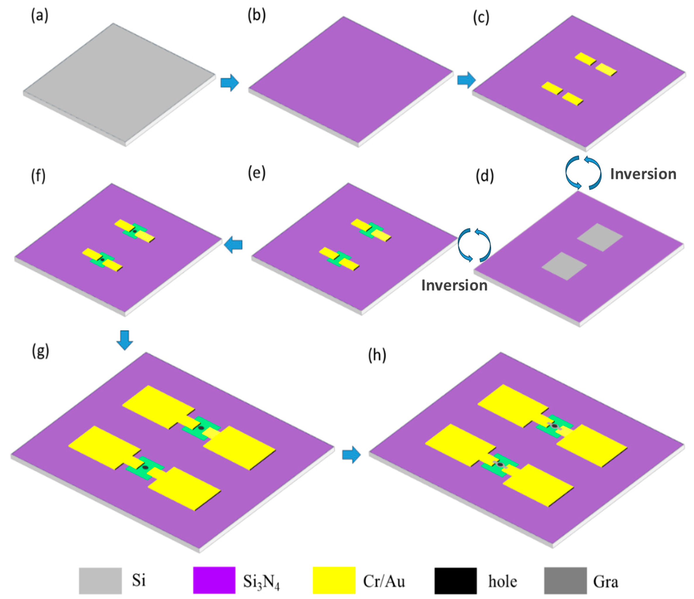
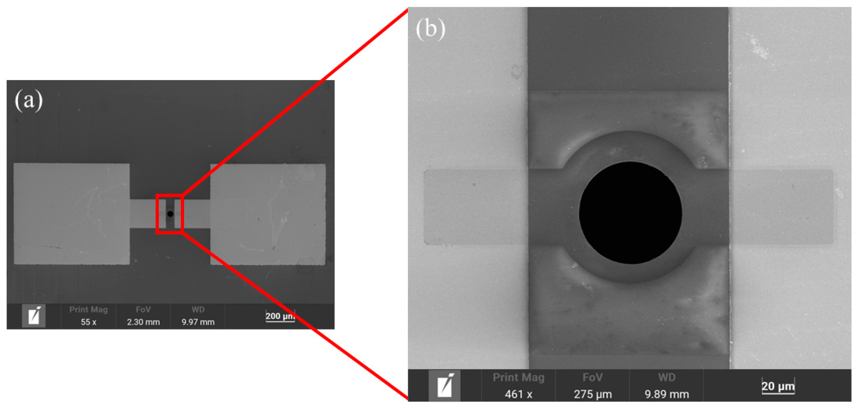
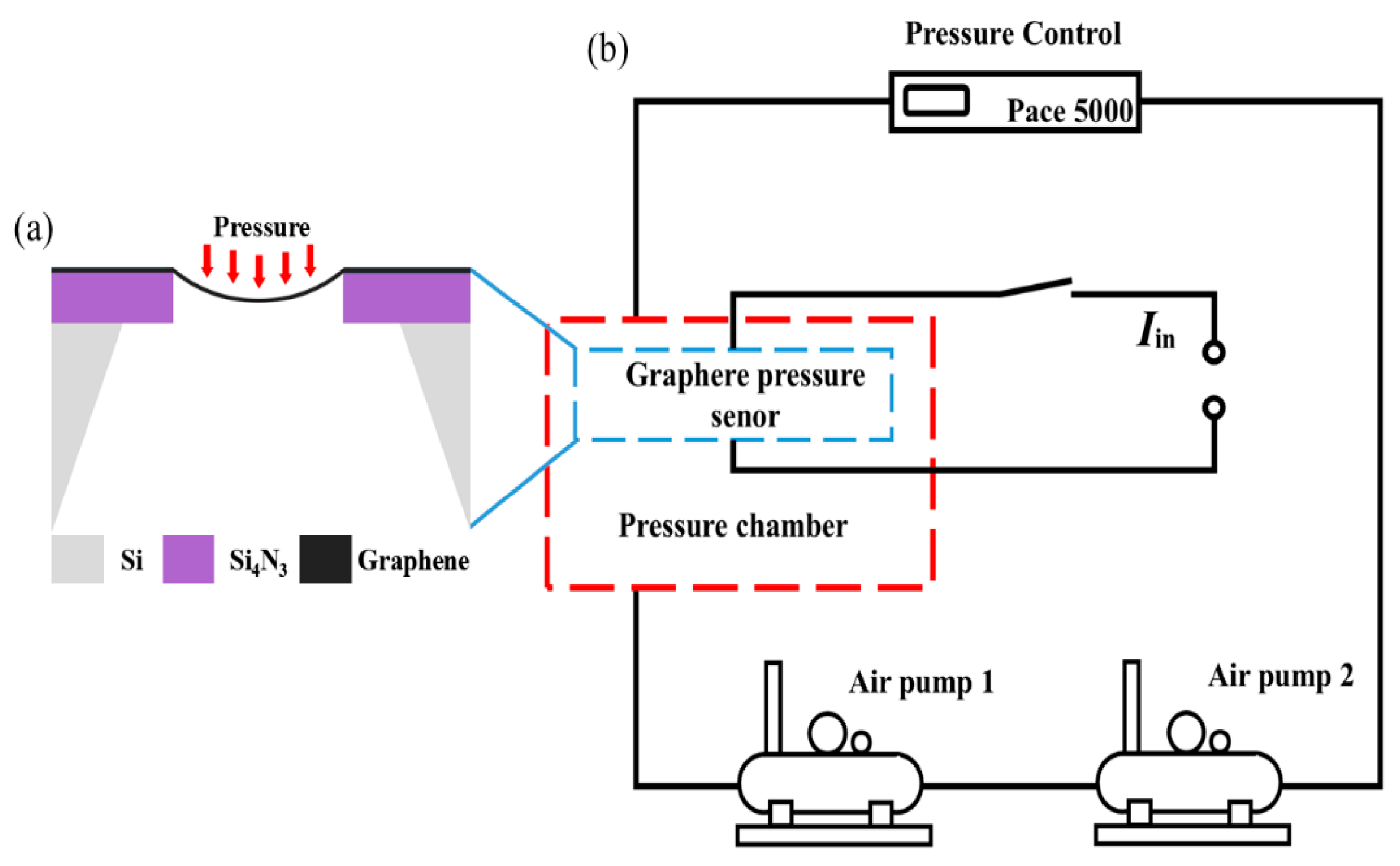
2. Sensor Fabrication
3. Experiment
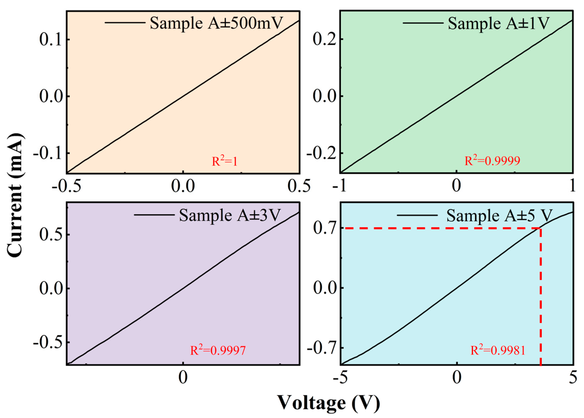
3.1. Voltammetry Characteristics of Graphene Devices
3.2. Current Resistance Characteristics
3.3. Current Piezoresistive Characteristics
4. Conclusions
Author Contributions
Funding
Institutional Review Board Statement
Informed Consent Statement
Data Availability Statement
Conflicts of Interest
Abbreviations
| LPCVD | Low Pressure Chemical Vapor Deposition |
| RIE | Reactive Ion Etching |
| SEM | Scanning Electron Microscope |
| PMMA | Polymethyl Methacrylate |
| AES | Auger Electron Spectroscopy |
| ID/IG | Intensity Ratio of D-band to G-band |
References
- Liu, G.; Jin, W.; Xu, N. Graphene-Based Membranes. Chem. Soc. Rev. 2015, 44, 5016–5030. [Google Scholar] [CrossRef] [PubMed]
- Lee, J.-H.; Lee, E.K.; Joo, W.-J.; Jang, Y.; Kim, B.-S.; Lim, J.Y.; Choi, S.-H.; Ahn, S.J.; Ahn, J.R.; Park, M.-H.; et al. Wafer-Scale Growth of Single-Crystal Monolayer Graphene on Reusable Hydrogen-Terminated Germanium. Science 2014, 344, 286–289. [Google Scholar] [CrossRef] [PubMed]
- Pumera, M. Graphene-Based Nanomaterials and Their Electrochemistry. Chem. Soc. Rev. 2010, 39, 4146. [Google Scholar] [CrossRef] [PubMed]
- Yang, Z.; Ren, J.; Zhang, Z.; Chen, X.; Guan, G.; Qiu, L.; Zhang, Y.; Peng, H. Recent Advancement of Nanostructured Carbon for Energy Applications. Chem. Rev. 2015, 115, 5159–5223. [Google Scholar] [CrossRef]
- Akinwande, D.; Brennan, C.J.; Bunch, J.S.; Egberts, P.; Felts, J.R.; Gao, H.; Huang, R.; Kim, J.-S.; Li, T.; Li, Y.; et al. A Review on Mechanics and Mechanical Properties of 2D Materials—Graphene and Beyond. Extrem. Mech. Lett. 2017, 13, 42–77. [Google Scholar] [CrossRef]
- Lou, Z.; Chen, S.; Wang, L.; Jiang, K.; Shen, G. An Ultra-Sensitive and Rapid Response Speed Graphene Pressure Sensors for Electronic Skin and Health Monitoring. Nano Energy 2016, 23, 7–14. [Google Scholar] [CrossRef]
- Smith, A.D.; Vaziri, S.; Niklaus, F.; Fischer, A.C.; Sterner, M.; Delin, A.; Östling, M.; Lemme, M.C. Pressure Sensors Based on Suspended Graphene Membranes. Solid-State Electron. 2013, 88, 89–94. [Google Scholar] [CrossRef]
- Zhang, G.-D.; Zhao, Y.-L.; Zhao, Y.; Wang, X.-C.; Wei, X.-Y. Research of a Novel Ultra-High Pressure Sensor with High-Temperature Resistance. Micromachines 2017, 9, 5. [Google Scholar] [CrossRef]
- Mo, C.; Tian, Z.; Wang, D. A Novel High-Performance MXene-Doped Graphene Pressure Sensor. IEEE Sens. J. 2024, 24, 14059–14067. [Google Scholar] [CrossRef]
- Nag, M.; Singh, J.; Kumar, A.; Singh, K. A High Sensitive Graphene Piezoresistive MEMS Pressure Sensor by Integration of Rod Beams in Silicon Diaphragm for Low Pressure Measurement Application. Microsyst. Technol. 2020, 26, 2971–2976. [Google Scholar] [CrossRef]
- Dolleman, R.J.; Davidovikj, D.; Cartamil-Bueno, S.J.; Van Der Zant, H.S.J.; Steeneken, P.G. Graphene Squeeze-Film Pressure Sensors. Nano Lett. 2016, 16, 568–571. [Google Scholar] [CrossRef] [PubMed]
- Chen, Y.-M.; He, S.-M.; Huang, C.-H.; Huang, C.-C.; Shih, W.-P.; Chu, C.-L.; Kong, J.; Li, J.; Su, C.-Y. Ultra-Large Suspended Graphene as a Highly Elastic Membrane for Capacitive Pressure Sensors. Nanoscale 2016, 8, 3555–3564. [Google Scholar] [CrossRef] [PubMed]
- Šiškins, M.; Lee, M.; Wehenkel, D.; Van Rijn, R.; De Jong, T.W.; Renshof, J.R.; Hopman, B.C.; Peters, W.S.J.M.; Davidovikj, D.; Van Der Zant, H.S.J.; et al. Sensitive Capacitive Pressure Sensors Based on Graphene Membrane Arrays. Microsyst. Nanoeng. 2020, 6, 102. [Google Scholar] [CrossRef]
- Romijn, J.; Dolleman, R.J.; Singh, M.; Van Der Zant, H.S.J.; Steeneken, P.G.; Sarro, P.M.; Vollebregt, S. Multi-Layer Graphene Pirani Pressure Sensors. Nanotechnology 2021, 32, 335501. [Google Scholar] [CrossRef] [PubMed]
- Song, H.; Kang, F. Recent Progress on Thermal Conduction of Graphene. Acta Phys. Chim. Sin. 2021, 38, 2101013. [Google Scholar] [CrossRef]
- Liu, D.; Chen, S.; Lu, Z.; Ma, N.; Sun, Y. Temperature Sensor Based on Temperature and Frequency Dependence of Graphene Impedance. J. Phys. Appl. Phys. 2019, 52, 075102. [Google Scholar] [CrossRef]
- Shao, Q.; Liu, G.; Teweldebrhan, D.; Balandin, A.A. High-Temperature Quenching of Electrical Resistance in Graphene Interconnects. Appl. Phys. Lett. 2008, 92, 202108. [Google Scholar] [CrossRef]
- Subrina, S. Heat Transport in Graphene Interconnect Networks With Graphene Lateral Heat Spreaders. IEEE Trans. Nanotechnol. 2012, 11, 777–781. [Google Scholar] [CrossRef]
- Pop, E. Energy Dissipation and Transport in Nanoscale Devices. Nano Res. 2010, 3, 147–169. [Google Scholar] [CrossRef]
- Choi, J.H.; Shin, D.H.; Inani, H.; Kwon, M.H.; Mustonen, K.; Mangler, C.; Park, M.; Jeong, H.; Lee, D.S.; Kotakoski, J.; et al. Transformation and Evaporation of Surface Adsorbents on a Graphene “Hot Plate”. ACS Appl. Mater. Interfaces 2020, 12, 26313–26319. [Google Scholar] [CrossRef]
- Durkan, C.; Xiao, Z. On the Failure of Graphene Devices by Joule Heating under Current Stressing Conditions. Appl. Phys. Lett. 2015, 107, 243505. [Google Scholar] [CrossRef]
- Solenov, D.; Velizhanin, K.A. Adsorbate Transport on Graphene by Electromigration. Phys. Rev. Lett. 2012, 109, 095504. [Google Scholar] [CrossRef] [PubMed]
- Ravi Chandran, K.S. Transient Joule Heating of Graphene, Nanowires and Filaments: Analytical Model for Current-Induced Temperature Evolution Including Substrate and End Effects. Int. J. Heat Mass Transf. 2015, 88, 14–19. [Google Scholar] [CrossRef]
- Moradi, Z.; Vaezzadeh, M.; Saeidi, M. Temperature-Dependent Thermal Expansion of Graphene. Phys. Stat. Mech. Its Appl. 2018, 512, 981–985. [Google Scholar] [CrossRef]
- He, H.; Pan, B. The Hydrogenation-Dependent Thermal Expansion Properties of Hydrogenated Graphene. Eur. Phys. J. B 2014, 87, 40. [Google Scholar] [CrossRef]
- Bondarev, V.N.; Adamyan, V.M.; Zavalniuk, V.V. Bending Mode and Thermal Expansion of Graphene. Phys. Rev. B 2018, 97, 035426. [Google Scholar] [CrossRef]
- Seol, J.H.; Jo, I.; Moore, A.L.; Lindsay, L.; Aitken, Z.H.; Pettes, M.T.; Li, X.; Yao, Z.; Huang, R.; Broido, D.; et al. Two-Dimensional Phonon Transport in Supported Graphene. Nano Lett. 2010, 10, 1645–1651. [Google Scholar] [CrossRef] [PubMed]
- Yalon, E.; Aslan, Ö.B.; Smithe, K.K.H.; McClellan, C.J.; Suryavanshi, S.V.; Xiong, F.; Sood, A.; Neumann, C.M.; Xu, X.; Goodson, K.E.; et al. Temperature-Dependent Thermal Boundary Conductance of Monolayer MoS2 by Raman Thermometry. ACS Appl. Mater. Interfaces 2017, 9, 43013–43020. [Google Scholar] [CrossRef]
- Watanabe, K.; Taniguchi, T.; Kanda, H. Direct-Bandgap Properties and Evidence for Ultraviolet Lasing of Hexagonal Boron Nitride Single Crystal. Nano Lett. 2013, 13, 550–554. [Google Scholar] [CrossRef]
- Li, X.; Kong, B.D.; Zavada, J.M.; Kim, K.W. Strong Substrate Effects of Joule Heating in Graphene Electronics. Appl. Phys. Lett. 2011, 99, 233114. [Google Scholar] [CrossRef]
- Tivanov, M.S.; Kolesov, E.A.; Korolik, O.V.; Saad, A.M.; Komissarov, I.V. Effect of the Substrate on Phonon Properties of Graphene Estimated by Raman Spectroscopy. J. Low Temp. Phys. 2018, 190, 20–25. [Google Scholar] [CrossRef]
- Kim, K.; Regan, W.; Geng, B.; Alemán, B.; Kessler, B.M.; Wang, F.; Crommie, M.F.; Zettl, A. High-temperature Stability of Suspended Single-layer Graphene. Phys. Status Solidi RRL—Rapid Res. Lett. 2010, 4, 302–304. [Google Scholar] [CrossRef]
- Seo, M.; Kim, D.-H.; Lee, J.-H.; Son, S.-K. Electronic-Temperature Estimation of Joule-Heated Graphene via Raman Investigations. J. Korean Phys. Soc. 2021, 78, 164–168. [Google Scholar] [CrossRef]
- Guo, X.; Wang, Y.; You, S.; Yang, D.; Jia, G.; Song, F.; Dou, W.; Huang, H. Substrate Effect on Phonon in Graphene Layers. Carbon Lett. 2023, 33, 1359–1365. [Google Scholar] [CrossRef]
- Cheng, Z.-F.; Zheng, R.-L. Thermal Expansion and Deformation of Graphene. Chin. Phys. Lett. 2016, 33, 046501. [Google Scholar] [CrossRef]


Disclaimer/Publisher’s Note: The statements, opinions and data contained in all publications are solely those of the individual author(s) and contributor(s) and not of MDPI and/or the editor(s). MDPI and/or the editor(s) disclaim responsibility for any injury to people or property resulting from any ideas, methods, instructions or products referred to in the content. |
© 2025 by the authors. Licensee MDPI, Basel, Switzerland. This article is an open access article distributed under the terms and conditions of the Creative Commons Attribution (CC BY) license (https://creativecommons.org/licenses/by/4.0/).
Share and Cite
Mi, H.; Qi, R.; Li, P.; Su, N.; Wang, J. Investigation of Current Effect of Suspended Graphene Pressure Sensor. Materials 2025, 18, 2801. https://doi.org/10.3390/ma18122801
Mi H, Qi R, Li P, Su N, Wang J. Investigation of Current Effect of Suspended Graphene Pressure Sensor. Materials. 2025; 18(12):2801. https://doi.org/10.3390/ma18122801
Chicago/Turabian StyleMi, Haowei, Run Qi, Pengcheng Li, Ningning Su, and Junqiang Wang. 2025. "Investigation of Current Effect of Suspended Graphene Pressure Sensor" Materials 18, no. 12: 2801. https://doi.org/10.3390/ma18122801
APA StyleMi, H., Qi, R., Li, P., Su, N., & Wang, J. (2025). Investigation of Current Effect of Suspended Graphene Pressure Sensor. Materials, 18(12), 2801. https://doi.org/10.3390/ma18122801