
Metal–Semiconductor Behavior along the Line of Stacking Order Change in Gated Multilayer Graphene

Abstract
1. Introduction
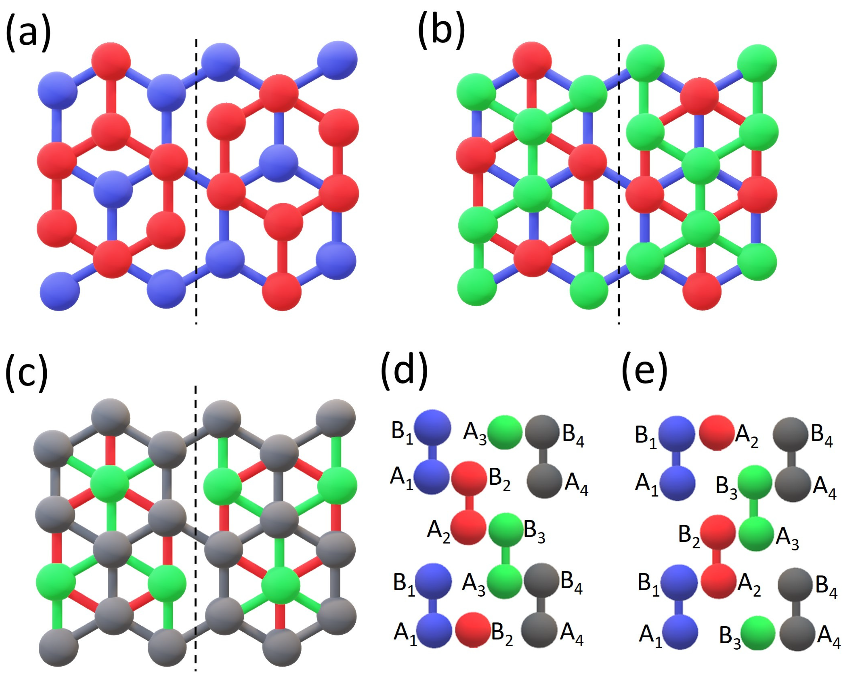
2. System and Method
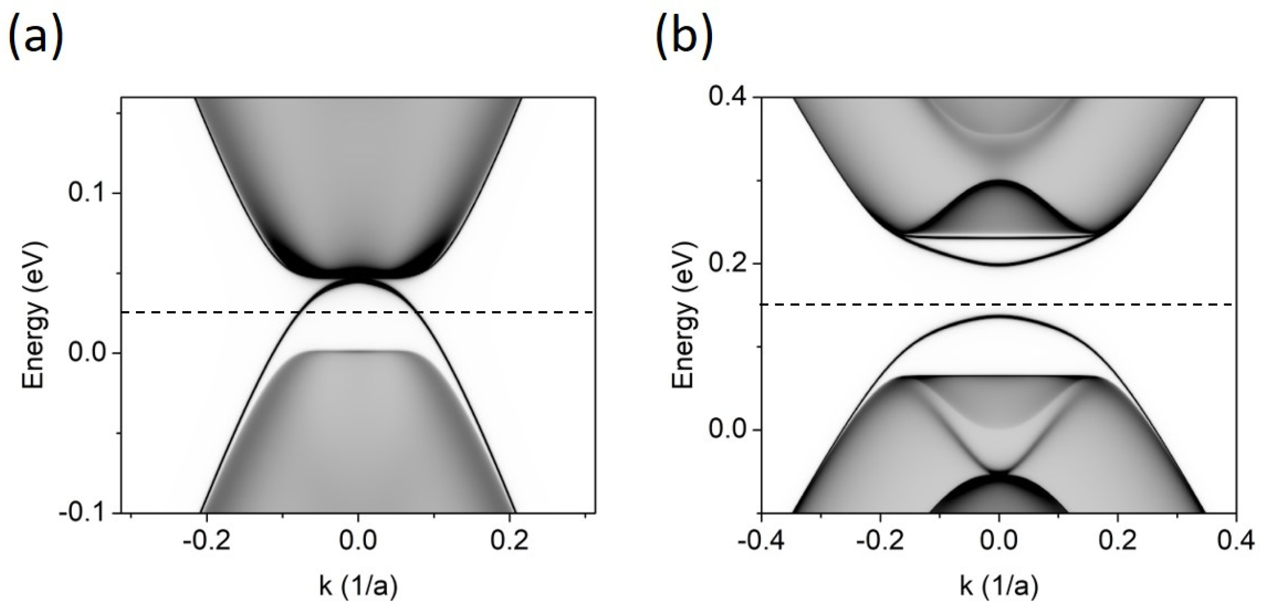
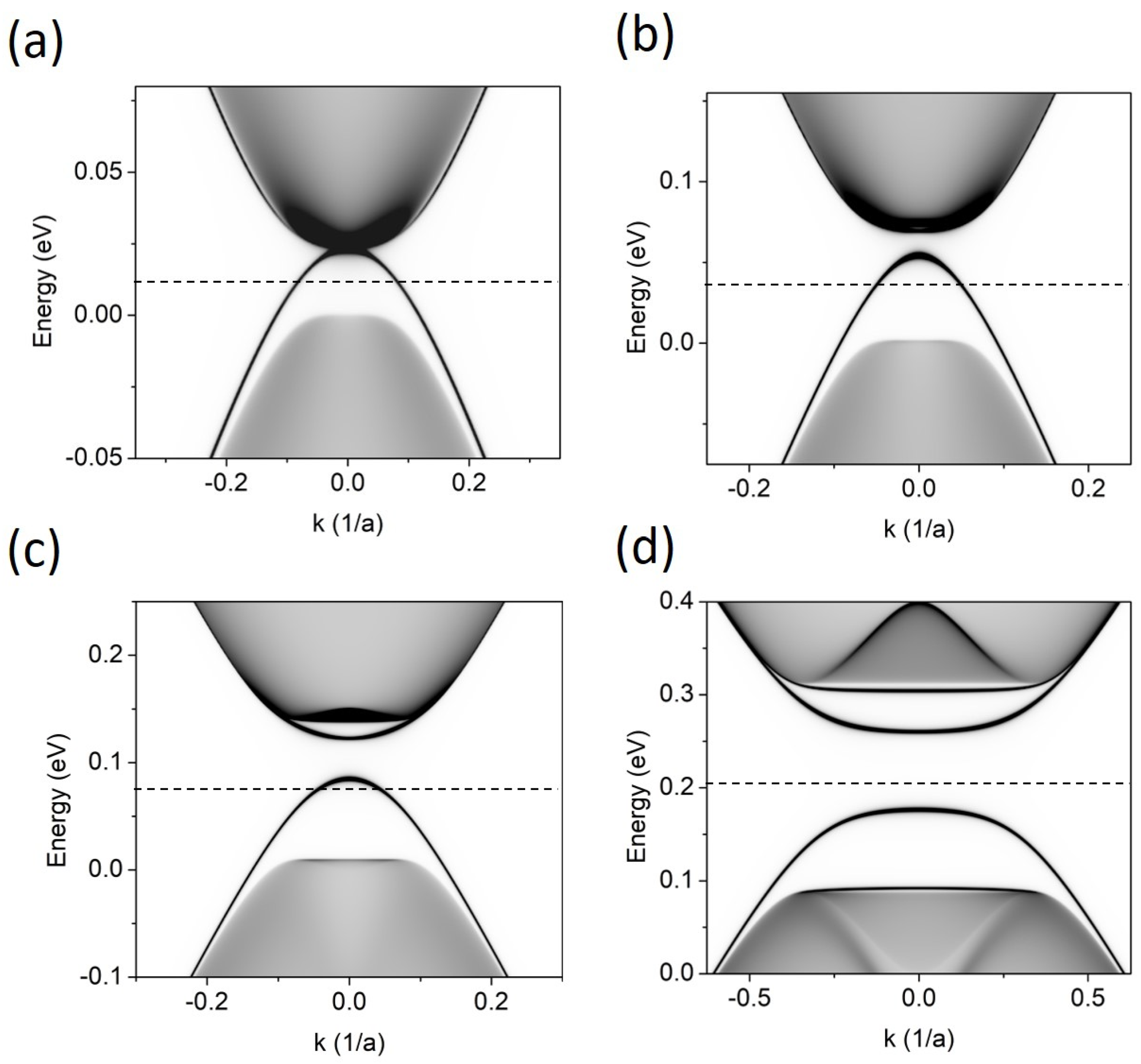
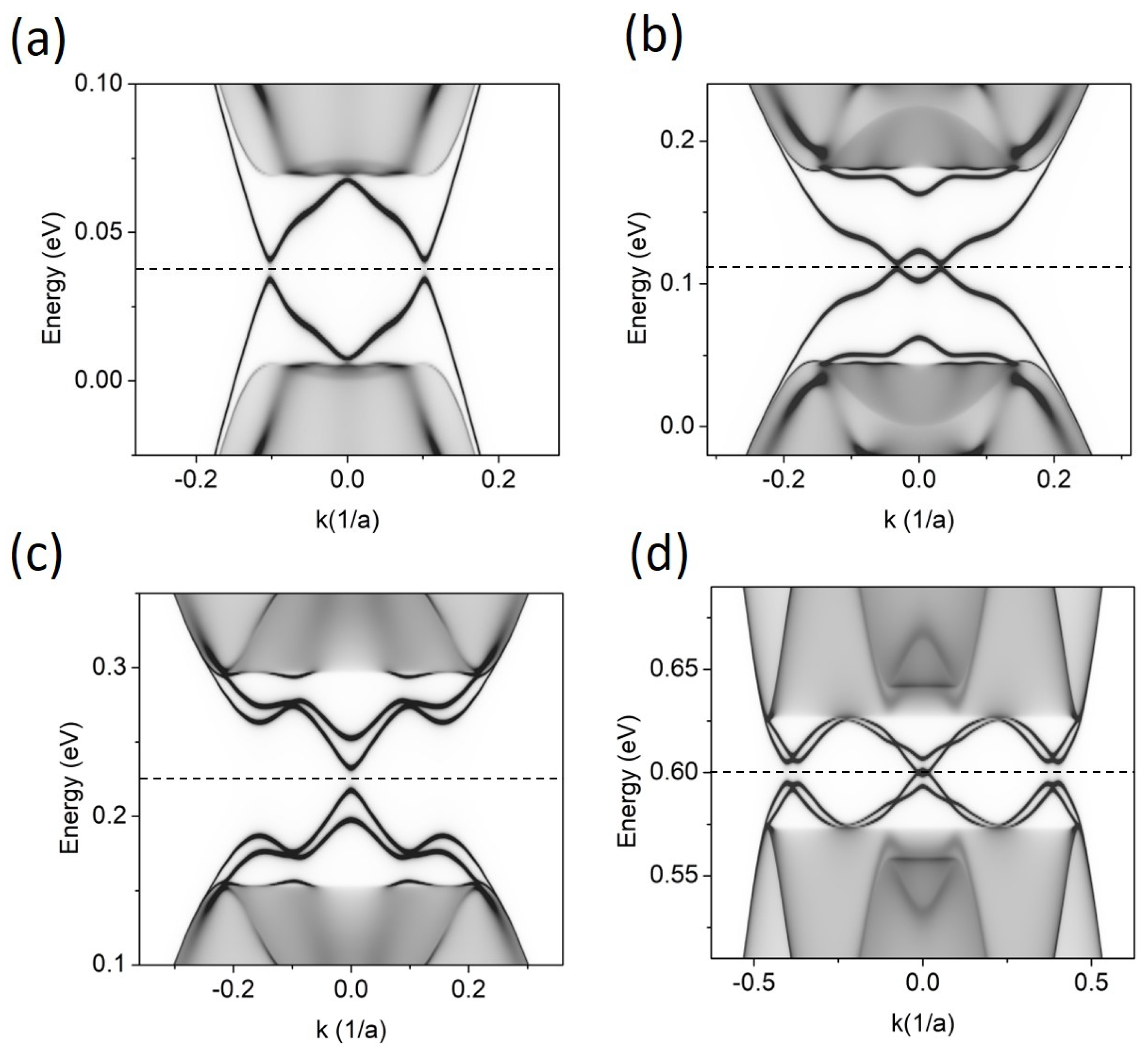
3. Results and Discussion
4. Conclusions
Funding
Institutional Review Board Statement
Informed Consent Statement
Data Availability Statement
Conflicts of Interest
References
- Ju, L.; Shi, Z.; Nair, N.; Lv, Y.; Jin, C.; Velasco, J., Jr.; Ojeda-Aristizabal, C.; Bechtel, H.A.; Martin, M.C.; Zettl, A.; et al. Topological valley transport at bilayer graphene domain walls. Nature 2015, 520, 650–655. [Google Scholar] [CrossRef] [PubMed]
- Pelc, M.; Jaskolski, W.; Ayuela, A.; Chico, L. Topologically confined states at corrugations of gated bilayer graphene. Phys. Rev. B 2015, 92, 085433. [Google Scholar] [CrossRef]
- Lane, T.L.M.; Andelkovic, J.; Wallbank, J.R.; Covaci, L.; Peeters, F.M.; Falko, V.I. Ballistic electron channels including weakly protected topological states in delaminated bilayer graphene. Phys. Rev. B 2018, 97, 045301. [Google Scholar] [CrossRef]
- Anderson, P.; Huang, Y.; Ayuela, A.; Fan, Y.; Oubbaj, S.; Coh, S.; Zhou, Q.; Ojeda-Aristizabal, C. Strain tuning of domain walls in multilayer graphene probed in the quantum Hall regime. Phys. Rev. B 2022, 105, L081408. [Google Scholar] [CrossRef]
- Vaezi, A.; Liang, D.; Nagi, D.H.; Yang, L.; Kim, E.-A. Topological Edge States at a Tilt Boundary of Gated Multilayer Graphene. Phys. Rev. X 2013, 3, 021018. [Google Scholar] [CrossRef]
- Zhang, F.; McDonald, A.H.; Mele, E.J. Valley Chern numbers and boundary modes in gapped bilayer graphene. Proc. Natl. Acad. Sci. USA 2013, 110, 10546–10551. [Google Scholar] [CrossRef] [PubMed]
- San-Jose, P.; Gorbachev, R.V.; Geim, A.K.; Novoselov, K.S.; Guinea, F. Stacking Boundaries and Transport in Bilayer Graphene. Nano Lett. 2014, 14, 2052–2057. [Google Scholar] [CrossRef] [PubMed]
- Jung, J.; Zhang, F.; Qiao, Z.; MacDonald, A.H. Valley-Hall kink and edge states in multilayer graphene. Phys. Rev. B 2011, 84, 075418. [Google Scholar] [CrossRef]
- Jaskolski, W. Electronic structure of trilayer graphene with internal layer broken. Mol. Phys. 2022, 120, e2013554. [Google Scholar] [CrossRef]
- Jaskolski, W. Gapless states and current control in strongly distorted gated trilayer graphene. Solid State Commun. 2023, 360, 115043. [Google Scholar] [CrossRef]
- Beitner, D.; Amiaty, S.; Atri, S.S.; McEllistrim, A.; Coen, T.; Falko, V.I.; Richter, S.; Shalom, M.B.; Suchowski, H. Mid-Infrared Mapping of Four-Layer Graphene Polytypes Using Near-Field Microscopy. Nano Lett. 2023, 23, 10758–10764. [Google Scholar] [CrossRef] [PubMed]
- Jang, B.; Kim, B.; Kim, J.-H.; Lee, H.-J.; Sumigawa, T.; Kitamura, T. Asynchronous cracking with dissimilar paths in multilayer graphene. Nanoscale 2017, 9, 17325–17333. [Google Scholar] [CrossRef] [PubMed]
- Yin, L.-J.; Jiang, H.; Qiao, J.-B.; He, L. Direct imaging edge states at a bilayer graphene domain wall. Nat. Commun. 2016, 7, 11760. [Google Scholar] [CrossRef] [PubMed]
- Zhang, F.; Sahu, B.; Min, H.; MacDonald, A.H. Band structure of ABC-stacked graphene trilayers. Phys. Rev. B 2010, 82, 035409. [Google Scholar] [CrossRef]
- Perez Riffo, F.; Vizcaya, S.; Menendez-Proupin, E.; Florez, J.M.; Chico, L.; Suarez Morell, E. Behavior of localized states in twisted ABC trilayer graphene. Carbon 2024, 222, 118952. [Google Scholar] [CrossRef]
- Zhang, F.; Jung, J.; Fiete, G.A.; Niu, Q.; MacDonald, A.H. Spontaneous Quantum Hall States in Chirally Stacked Few-Layer Graphene Systems. Phys. Rev. Lett. 2011, 106, 156801. [Google Scholar] [CrossRef] [PubMed]
- Chittari, B.L.; Chen, G.; Zhang, Y.; Wang, F.; Jung, J. Gate-Tunable Topological Flat Bands in Trilayer Graphene Boron-Nitride Moire Superlattices. Phys. Rev. Lett. 2019, 122, 016401. [Google Scholar] [CrossRef] [PubMed]
- Nardelli, M.B. Electronic transport in extended systems: Application to carbon nanotubes. Phys. Rev. B 1999, 60, 7828–7833. [Google Scholar] [CrossRef]
- Castro, E.V.; Novoselov, K.S.; Morozov, S.V.; Peres, N.M.R.; Lopes dos Santos, J.M.B.; Nilsson, J.; Guinea, F.; Geim, A.K.; Castro Neto, A.H. Biased Bilayer Graphene: Semiconductor with a Gap Tunable by the Electric Field Effect. Phys. Rev. Lett. 2007, 99, 216802. [Google Scholar] [CrossRef]
- Ohta, T.; Bostwick, A.; Seyller, T.; Horn, K.; Rotenberg, E. Controlling the Electronic Structure of Bilayer Graphene. Science 2003, 313, 951–954. [Google Scholar] [CrossRef]
- Jaskolski, W.; Pelc, M.; Chico, L.; Ayuela, A. Existence of nontrivial topologically protected states at grain boundaries in bilayer graphene: Signatures and electrical switching. Nanoscale 2016, 8, 6079–6084. [Google Scholar] [CrossRef]
- Jaskolski, W.; Pelc, M.; Bryant, G.W.; Chico, L.; Ayuela, A. Controlling the layer localization of gapless states in bilayer graphene with a gate voltage. 2D Materials 2018, 5, 025006. [Google Scholar] [CrossRef]
- Li, J.; Wang, K.; McFaul, K.J.; Zern, Z.; Ren, Y.; Watanabe, K.; Taniguchi, T.; Qiao, Z.; Zhu, J. Gate-controlled conducting channels in bilayer graphene. Nat. Nanotechnol. 2016, 11, 1060–1065. [Google Scholar] [CrossRef]
- de Sena, S.H.R.; Pereira, J.M.; Peeters, F.M.; Farais, G.A. Topological confinement in trilayer graphene. Phys. Rev. B 2014, 89, 035420. [Google Scholar] [CrossRef]
- Silkin, V.M.; Kogan, E.; Gumbs, G. Screening in Graphene: Response to External Static Electric Field and an Image-Potential Problem. Nanomaterials 2021, 11, 1561. [Google Scholar] [CrossRef] [PubMed]
- Yu, E.K.; Stewart, D.A.; Tiwari, S. Ab initio study of polarizability and induced charge densities in multilayer graphene films. Phys. Rev. B 2008, 77, 195406. [Google Scholar] [CrossRef]
- Wang, R.-N.; Dong, G.-Y.; Wang, S.-F.; Fu, G.-S.; Wang, J.-L. Intra- and Inter-layer charge redistribution in biased bilayer graphene. AIP Adv. 2016, 6, 035213. [Google Scholar] [CrossRef]
- Luo, W.; Yan, X.; Pan, X.; Jiao, J.; Mai, L. What Makes On-Chip Microdevices Stand Out in Electrocatalysis? Small 2024, 20, 2305020. [Google Scholar] [CrossRef] [PubMed]
- Kusakabe, K. Flat-band Ferromagnetism in Organic Crystals. In Carbon Based Magnetism; Makarova, T.L., Palacio, F., Eds.; Elsevier: Amsterdam, The Netherlands, 2007; pp. 305–328. [Google Scholar]
- Bouzerar, G. Flat band induced room-temperature ferromagnetism in two-dimensional systems. Phys. Rev. B 2023, 107, 184441. [Google Scholar] [CrossRef]
- Sawada, K.; Ishii, F.; Saito, M. First-principles study of carrier-induced ferromagnetism in bilayer and multilayer zigzag graphene nanoribbons. App. Phys. Lett. 2014, 104, 143111. [Google Scholar] [CrossRef]
- Pons, R.; Mielke, A.; Stauber, T. Flat-band ferromagnetism in twisted bilayer graphene. Phys. Rev. B 2020, 102, 235101. [Google Scholar] [CrossRef]
- Cao, Y.; Fatemi, V.; Fang, S.; Watanabe, K.; Taniguchi, T.; Kaxiras, E.; Jarillo-Herrero, P. Unconventional superconductivity in magic-angle graphene superlattices. Nature 2018, 556, 43–50. [Google Scholar] [CrossRef] [PubMed]
- Han, T.; Lu, Z.; Scuri, G.; Sung, J.; Wang, J.; Han, T.; Watanabe, K.; Taniguchi, T.; Park, H.; Ju, L. Correlated insulator and Chern insulators in pentalayer rhombohedral-stacked graphene. Nature Nanotechnol. 2023, 19, 181–187. [Google Scholar] [CrossRef] [PubMed]
- Yin, L.-J.; Yang, L.-Z.; Zhang, L.; Wu, Q.; Fu, X.; Tong, L.-H.; Yang, G.; Tian, Y.; Zhang, L.; Qin, Z. Imaging of nearly flat induced atomic-scale negative differential conductivity in ABC-stacked trilayer graphene. Phys. Rev. B 2020, 102, 241403. [Google Scholar] [CrossRef]
- Pantaleon, P.A.; Jimeno-Pozo, A.; Sainz-Cruz, H.; Phong, V.T.; Cea, T.; Guinea, F. Superconductivity and correlated phases in non-twisted bilayer and trilayer graphene. Nat. Rev. Phys. 2023, 5, 304–315. [Google Scholar] [CrossRef]


Disclaimer/Publisher’s Note: The statements, opinions and data contained in all publications are solely those of the individual author(s) and contributor(s) and not of MDPI and/or the editor(s). MDPI and/or the editor(s) disclaim responsibility for any injury to people or property resulting from any ideas, methods, instructions or products referred to in the content. |
© 2024 by the author. Licensee MDPI, Basel, Switzerland. This article is an open access article distributed under the terms and conditions of the Creative Commons Attribution (CC BY) license (https://creativecommons.org/licenses/by/4.0/).
Share and Cite
Jaskólski, W. Metal–Semiconductor Behavior along the Line of Stacking Order Change in Gated Multilayer Graphene. Materials 2024, 17, 1915. https://doi.org/10.3390/ma17081915
Jaskólski W. Metal–Semiconductor Behavior along the Line of Stacking Order Change in Gated Multilayer Graphene. Materials. 2024; 17(8):1915. https://doi.org/10.3390/ma17081915
Chicago/Turabian StyleJaskólski, Włodzimierz. 2024. "Metal–Semiconductor Behavior along the Line of Stacking Order Change in Gated Multilayer Graphene" Materials 17, no. 8: 1915. https://doi.org/10.3390/ma17081915
APA StyleJaskólski, W. (2024). Metal–Semiconductor Behavior along the Line of Stacking Order Change in Gated Multilayer Graphene. Materials, 17(8), 1915. https://doi.org/10.3390/ma17081915