1. Introduction
Metamaterials are artificially designed arrays of sub-wavelength microstructures capable of manipulating electromagnetic waves arbitrarily through the free design of microstructures. Specifically, metamaterials can achieve anomalous and novel electromagnetic phenomena not attainable in traditional materials, sparking extensive research interest in electromagnetic manipulation [
1,
2]. Metasurfaces, on the other hand, are two-dimensional metamaterials comprised of subwavelength periodic arrays with ultra-thin thickness, offering advantages such as easy processing, low loss, and an ultra-compact configuration [
3,
4]. As a ubiquitous phenomenon observed in various systems, coupling phenomenon profoundly alters the original oscillation state of resonant systems and leads to unique optical properties [
5,
6]. In the realm of metasurfaces, coupling effects have been demonstrated to significantly modify the behavior of resonant systems, resulting in enhanced optical characteristics. For instance, coupling has been instrumental in facilitating well-known physical phenomena such as electromagnetically induced transparency (EIT) [
7,
8], Fano resonance [
9,
10], and so forth., In particular, EIT manifests as a narrow transparency window within the original absorption spectrum. Owing to its promising applications, EIT has garnered significant attention in the optical field, including enhanced transmission windows and strong dispersion characteristics. However, previous EIT devices have displayed fixed functionalities once the proposed metasurfaces were fabricated, constraining their broadened applications. In this study, we have introduced dynamically controlled terahertz (THz) metasurfaces based on elementary cells with tunable optical properties to overcome these limitations [
11,
12]. Previous studies have incorporated phase change materials into metasurfaces to achieve dynamic functionality. Among the commonly used phase change materials, vanadium dioxide (VO
2) is a more suitable candidate due to the relatively low excitation threshold of external stimulus [
13,
14]. Particularly, VO
2 undergoes a reversible insulator-to-metal transition (IMT) around room temperature (68 °C), making it an ideal choice for developing dynamically controlled energy efficient devices. Therefore, the metal–insulator phase transitions of VO
2 in metasurfaces have become a research hotspot in the design dynamically controlled THz metasurfaces.
In 2019, Xingbo Liu et al. proposed temperature-controlled THz holography based on the phase transition of VO
2 [
15]. Through the deposition of VO
2 under C-shaped split-ring resonators, the conductivity of VO
2 can be dynamically modulated by adjusting the operating temperature. This leads to a modification of the resonant properties of the split-ring resonators (SRRs) and the reconstruction of the holographic image. This innovative approach provides a dynamic and tunable method for controlling holography, showcasing potential practical applications in fields such as display technology and data storage. In 2013, Xueqian Zhang et al. introduced a polarization-independent EIT THz metasurface. The proposed metasurface unit cell comprises a cross and four identical SRRs positioned at equal distances within the four quadrants formed by the cross. This configuration exhibits four-fold rotational symmetry (C
4 symmetry) and manifests EIT electromagnetic properties through the coupling effect of four distinct modes [
16]. C
4 symmetry structures possess rotational symmetry that cannot be superimposed with their mirror image through simple rotation or translation. As a result, C
4 symmetry structures are frequently employed in the design of chiral metasurfaces, such as 4-U-SRRs [
15], corner-stacked rods [
17], conjugated gamma resonator pairs [
18], among others. Chiral metasurfaces have been demonstrated to have wide-ranging applications, including biological monitoring [
19], nonlinear enhancement [
20], circular polarizers [
21], and so on [
22,
23].
Previous studies (Xueqian Zhang et al.) have demonstrated that the EIT structure conforms to C
4 symmetry and is characterized by the coupling of four distinct modes [
16]. This approach acknowledges that EIT typically arises from the coupling between bright and dark modes. The bright mode is stimulated by incident radiation, whereas the dark mode is excited by the near-field coupling originating from the resonator of the bright mode. Utilizing this classical C
4 symmetric structure as a foundation, we exert control over the coupling in the structure by incorporating phase change materials.
In this research, we experimentally demonstrated a C4 symmetry-broken EIT structure by designing VO2 split-ring resonators (SRRs) or rings beneath the surface metal SRRs. The original C4 symmetry EIT structure consists of a cross and four identical SRRs, exhibiting four distinct modes: super-radiance mode (SM), superdark mode (DM), subradiance mode (sM), and subdark mode (dM). In our design, VO2 rings were inserted under one, two, three, and four SRRs, respectively, with their conductivity can be actively controlled through temperature regulation. By tailoring the conductivity of VO2, the C4 symmetry of the EIT structure is disrupted, resulting in modifications to the sM and dM structures. Consequently, the internal coupling modes of the C4 symmetry EIT structure were manipulated accordingly. In the following sections, we will delve into the impact of VO2 on inter-mode coupling in the EIT structure through detailed analyses of experimental and simulation results for VO2 rings designed beneath one, two, three, and four surface metal SRRs, respectively.
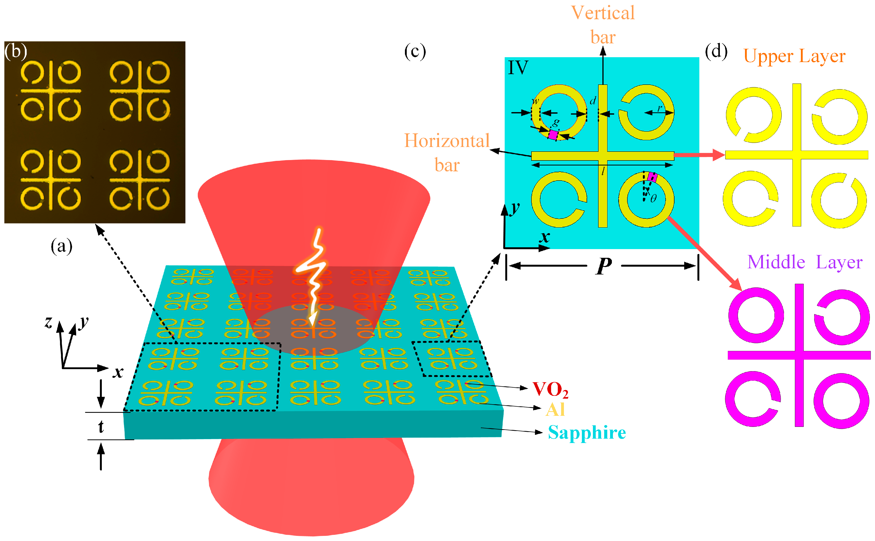
2. Device Design and Simulation Results
The proposed tunable C
4-symmetry-broken metasurfaces are structured in three layers, as illustrated in
Figure 1. The upper layer comprises aluminum (Al) metallic crosses and split-ring resonators (SRRs). In the middle layer, VO
2 crosses, SRRs, and rings are arranged. The SRRs are arranged to conform to C
4 symmetry and are distributed in four quadrants. The linewidths of VO
2 crosses, SRRs, and rings match that of the metallic crosses and SRRs. The lower layer consists of a C-cut sapphire substrate.
Various combinations of VO2 rings and SRRs have been used to design six different structures: (I) All VO2 SRRs are placed in the four quadrants. (II) One VO2 ring is positioned in the first quadrant, while VO2 SRRs occupy the other quadrants. (III) Two VO2 rings are located in the first and second quadrants, with two VO2 SRRs in the third and fourth quadrants. (IV) Two VO2 rings are positioned in the second and fourth quadrants, with two VO2 SRRs in the first and third quadrants. (V) Three VO2 rings occupy the first to third quadrants, while one VO2 SRR is placed in the fourth quadrant. (VI) Four VO2 rings are distributed across all quadrants.
The geometric parameters of the proposed C
4-symmetry-broken EIT metastructure are provided in
Figure 1c. The cross length is
l = 82 µm, and the width of all metal wires is
w = 5 µm. The outer radius of SRRs and rings is
r = 16 µm, and the gap width is
g = 5 µm. The relative center distance from an SRR or ring to a cross in the four quadrants is
d = 25 µm, respectively. The gap of the SRRs is at an angle of
θ = 15° with respect to the adjacent bars of the cross. The period of the unit cell is
P = 120 µm, and the substrate thickness is
t = 640 µm. The thickness of VO
2 layer and Al layer are both 200 nm. The conductivity of Al is set to 3.56 × 10
7 S/m, and the relative dielectric constant of C-cut sapphire is
ε = 9.4. The period
P of the unit cell is much smaller than the operation wavelength.
As a phase change material, VO
2 film undergoes a transition from monoclinic to tetragonal phases when heated from low to high temperatures. This phase change occurs rapidly around the critical temperature (TC = 68 °C), leading to significant alterations in the lattice structure. During this transition, various parameters of VO
2 thin films undergo substantial changes, such as transmittance, absorptivity, reflectivity, conductivity, refractive index, and magnetic susceptibility. The bulk conductivity of single-crystal VO
2 thin films can reach four orders of magnitude or higher. This conductivity change is attributed to the distortion of the VO
2 crystal lattice at the critical temperature, which alters the periodic potential and affects the crystal’s energy band structure. The lattice distortion in VO
2 thin films induces the splitting and movement of three-dimensional electronic states parallel to the C-axis of the tetragonal rutile phase. As a result, the Fermi level shifts from the original conduction band to the forbidden band, facilitating the transition from insulator to metal. The phase transition temperature of VO
2, occurring at 68 °C, aligns closely with room temperature, making the electrical and optical characteristics of VO
2 films grown on sapphire substrates abrupt. These characteristics, resembling those of crystal materials, provide VO
2 films with broad applications in temperature sensing, optics, and intelligent electrical switches. Achieving the phase transition of VO
2 is possible through electronic control and thermology. Under thermal control, VO
2 can reversibly transition from an insulating state to a metallic state. In our simulations, we utilized VO
2 conductivity σ = 200 S/m at 25 °C to replicate the transmission characteristics of the metasurface at room temperature and σ = 2 × 10
5 S/m at 68 °C to simulate the transmission characteristics at high temperature [
24,
25,
26,
27].
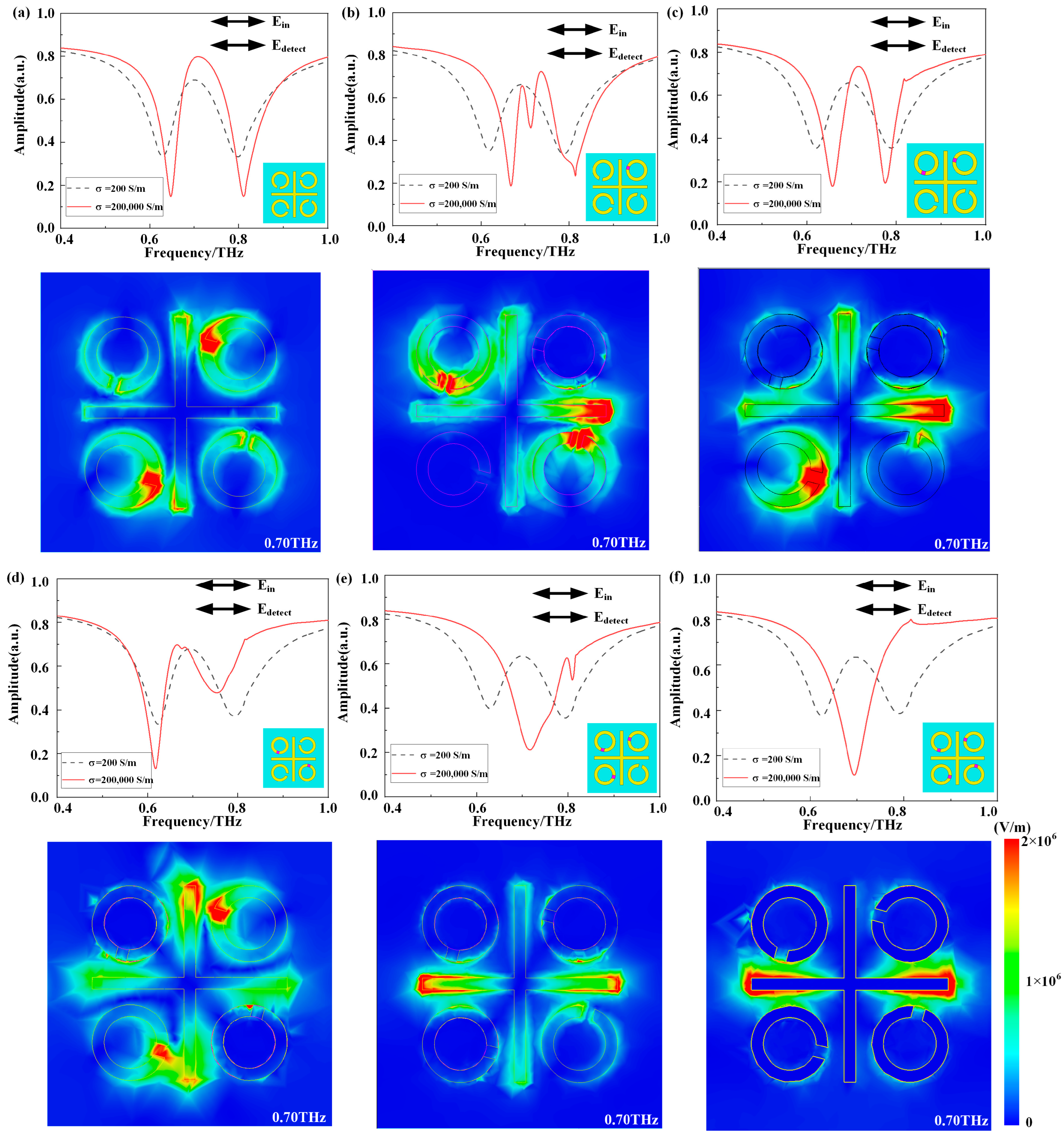
We analyzed the internal coupling modes of the C
4 symmetry-broken EIT structure for each model through simulation. Numerical simulations were performed using CST Microwave Studio 2019, a three-dimensional finite element electromagnetic simulation software. The boundary conditions were set as ±x and ±y directions as unit cells and ±z as open. We utilized a frequency domain solver of CST Microwave Studio 2019 for steady-state calculations. Sapphire and aluminum materials utilize default material parameters in CST Microwave Studio, while VO
2 employs the Drude model. The grid structure was configured using a hexagonal grid. At the EIT coupling mode of 0.70 THz,
Figure 2a illustrates the stimulation and coupling between SM (i.e., the horizontal bar) and DM (i.e., the vertical bar), dM (i.e., the SRRs in the first and third quadrant), and sM (i.e., the SRRs in the second and fourth quadrant), leading to the EIT phenomenon. In
Figure 2b at the same coupling mode, SM (i.e., the horizontal bar) was stimulated and coupled with DM (i.e., the vertical bar), dM (i.e., the SRRs in the third quadrant), and sM (i.e., the SRRs in the second and fourth quadrant), resulting in an incomplete EIT phenomenon. The electric field simulations in
Figure 2c indicate that EIT coupling primarily occurs between SM (i.e., the horizontal bar), DM (i.e., the vertical bar), dM (i.e., the SRR in the third quadrant), and sM (i.e., the SRR in the fourth quadrant), resulting in a relatively complete EIT peak due to left–right symmetry.
Figure 2d depicts SM (i.e., the horizontal bar) coupled with dM (i.e., the SRRs in the first and third quadrants) and DM (i.e., the vertical bar). In
Figure 2e, two resonance modes without an EIT phenomenon are observed—SM (i.e., the horizontal bar) and sM (i.e., the SRR in the fourth quadrant). At 0.70 THz, the primary resonance mode triggered by SM (i.e., the horizontal bar) produces a peak, while sM’s resonance is relatively weaker. Finally,
Figure 2f confirms, through transmission spectra and electric field simulation outcomes, that only SM (i.e., the horizontal bar) is directly triggered, resulting in a resonance peak at 0.70 THz. The analysis of the transmission spectra and electric fields for the
x-polarized incident waves highlights that the EIT phenomenon primarily relies on the coupling between SM and dM. Nevertheless, due to the non-coplanar nature of the VO
2 and metal structures, a height difference of 200 nm arises. Consequently, the electric field simulation results still exhibit the presence of an SRR. Despite this, the metal thickness is minimal, and the electric field at the opening is weak, ensuring negligible impact on the overall results.
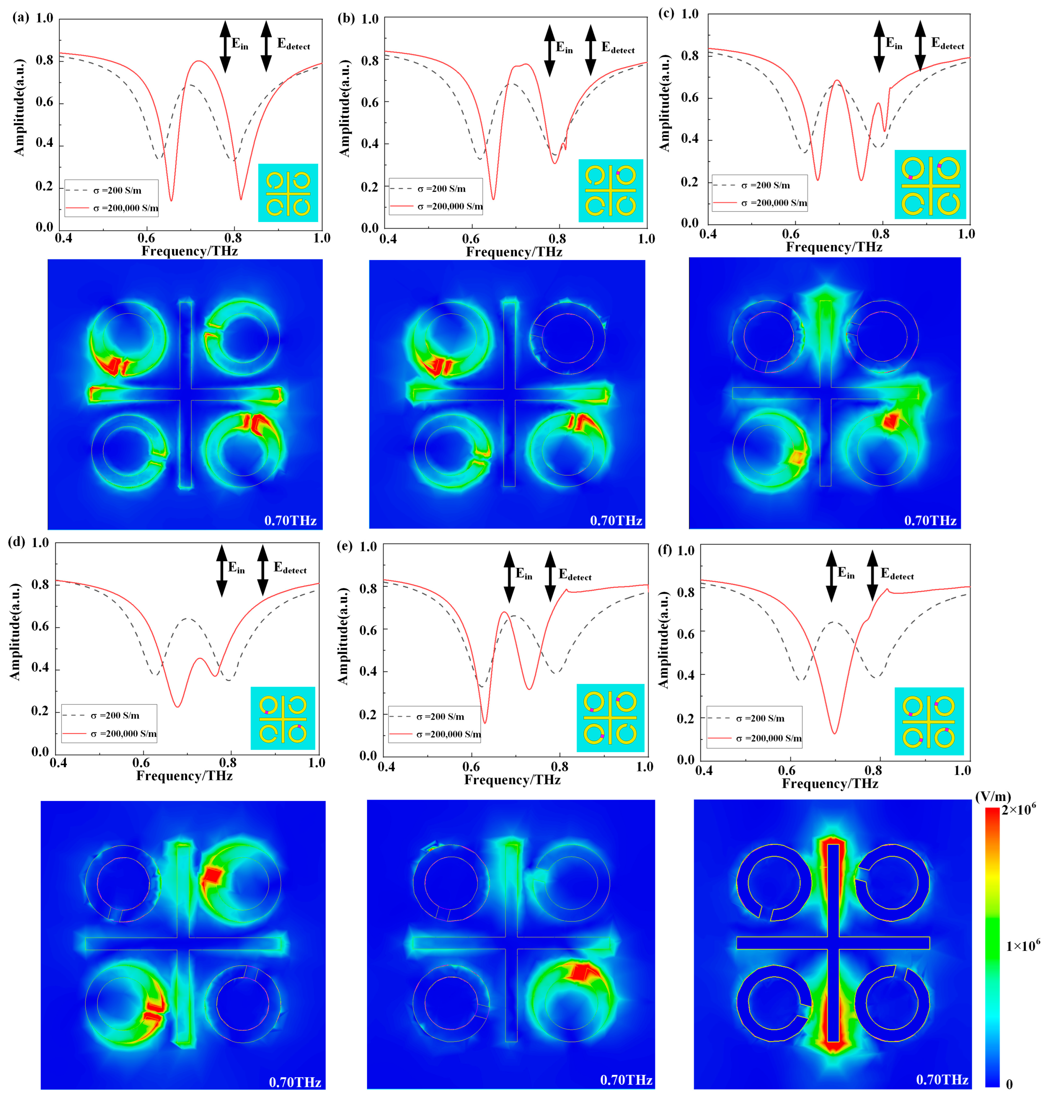
In
Figure 3a at the EIT coupling mode of 0.70 THz, the vertical bar (SM) is stimulated and coupled with the horizontal bar (DM), dM (i.e., the SRRs in the second and fourth quadrant), and sM (i.e., the SRRs in the first and third quadrant), leading to the EIT phenomenon.
Figure 3b shows that at the EIT coupling mode of 0.70 THz, SM (i.e., the vertical bar) is stimulated and coupled with DM (i.e., the horizontal bar), dM (i.e., the SRRs in the second and fourth quadrant), and sM (i.e., the SRRs in the third quadrant), resulting in an incomplete EIT phenomenon. In
Figure 3c, the electric field simulation results indicate that EIT coupling mainly occurs between SM (i.e., the vertical bar), DM (i.e., the horizontal bar), dM (i.e., the SRR in the fourth quadrant), and sM (i.e., the SRR in the third quadrant). Due to left–right symmetry, the EIT peak is relatively complete.
Figure 3d depicts SM (i.e., the vertical bar) weakly coupled with sM (i.e., the SRRs in the first and third quadrants) and DM (i.e., the horizontal bar). In
Figure 3e, at the EIT coupling mode, SM (i.e., the vertical bar) is stimulated and coupled with DM (i.e., the horizontal bar) and dM (i.e., the SRR in the fourth quadrant), resulting in an incomplete EIT phenomenon. Finally,
Figure 3f confirms, through the analysis of transmission spectra and electric field simulation outcomes, that only SM (i.e., the vertical bar) is directly triggered, producing a resonance peak at 0.70 THz. The analysis of the transmission spectra and electric fields for the
y-polarized incident waves further verifies the EIT phenomenon based on the coupling between SM and dM.
3. Experimental Verification
The metasurfaces were primarily fabricated using semiconductor device processing technology for metal and dielectric THz metasurfaces. The process began with depositing a layer of VO2 on a sapphire substrate. Subsequently, a uniform layer of photoresist was applied, and an optimal pattern was obtained through exposure and immersion in a developing solution. Following this, the VO2 layer underwent etching using reactive ion etching (RIE) with CF4. Finally, the aluminum metal structure was prepared through an etching process.
During the metasurfaces’ characterization, the THz time domain spectroscopy (TDS) system was employed to assess the transmission characteristics of the sample. To analyze the sample’s transmission characteristics at high temperatures, heating was facilitated using a perforated hot plate. To ensure the completion of the phase transition in VO2 within the structure, the temperature of the hot plate was set to 100 °C.
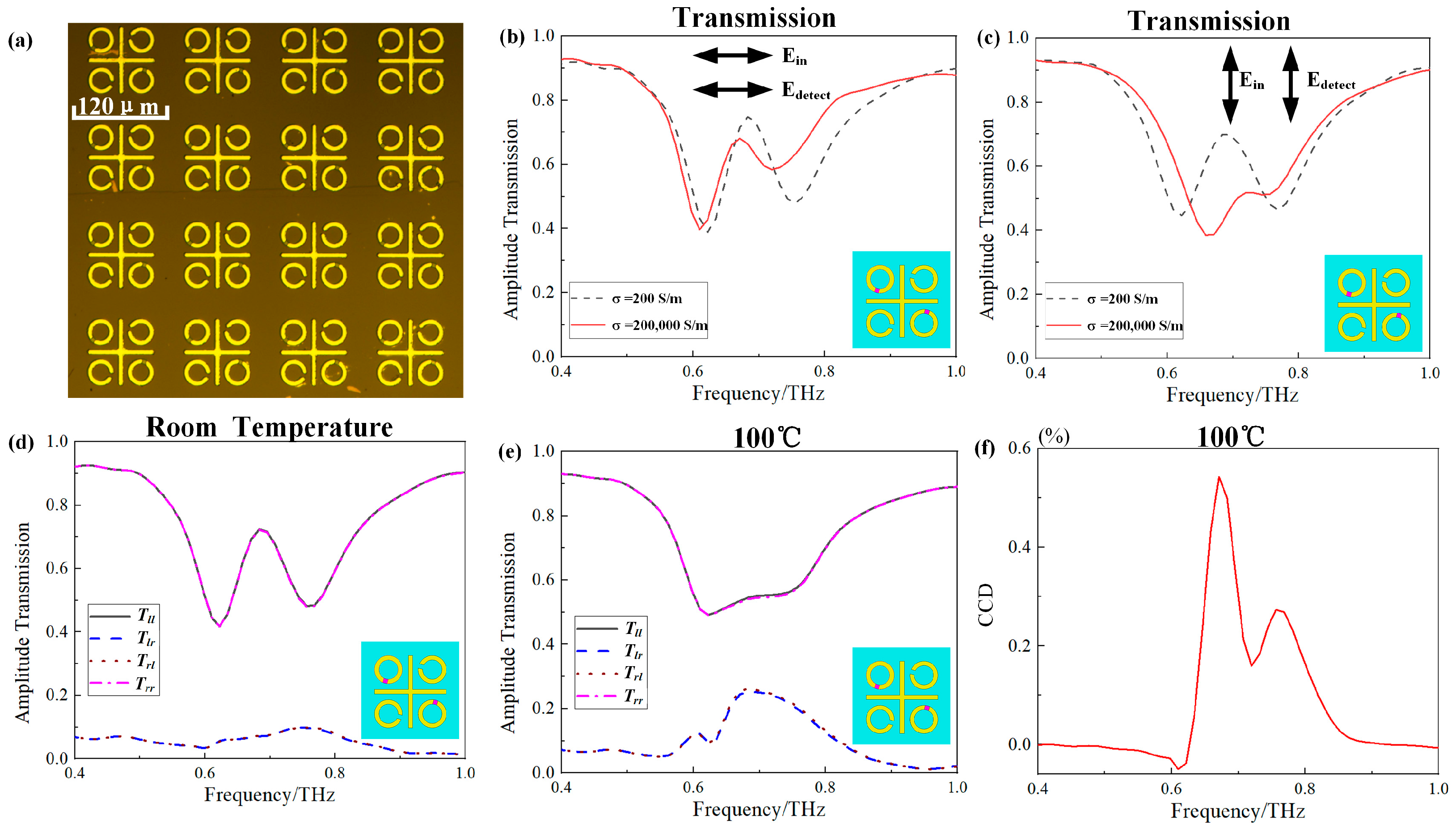
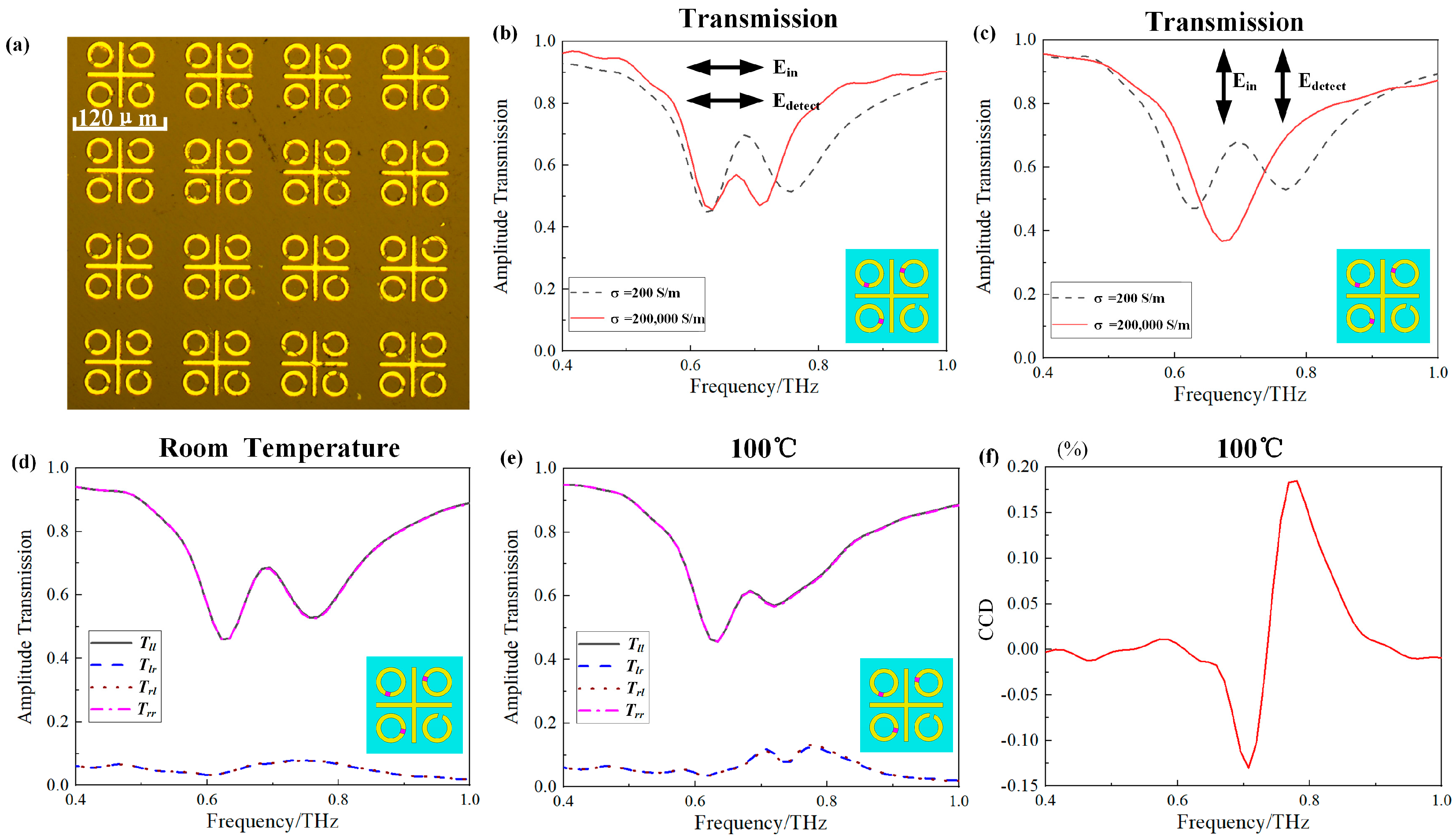
Figure 4a displays a partial microscopic image of the fabricated tunable C
4-symmetry-broken metasurfaces. During the fabrication process, the samples were initially grown using the molecular beam epitaxy method. Subsequently, a 200 nm thick VO
2 layer was deposited on a 640 µm thick C-cut sapphire substrate. To achieve the desired VO
2 structure, a combination of deep RIE and traditional lithography technology was utilized to etch the VO
2 layer of these devices. The metallic structures were created through the traditional lithography process, followed by deposition of a 200 nm thick aluminum film on the metallization. The microscopic image in
Figure 3a indicates that both the VO
2 structure and the metallic structure were fabricated with high quality.
To validate the accuracy of the simulation results, we conducted experimental measurements on the third and fourth models. Initially, we measured the transmission amplitudes of these models.
Figure 4b,c displays the transmission amplitude spectra with the
y-polarized and
x-polarized incident waves of the third model at both room temperature and 100 °C. The simulation results exhibit good agreement with the experimental results. Furthermore, we measured the spectral transmission response with circular-polarized incident waves for the third model at both room temperature and 100 °C.
Figure 4d,e illustrates the transmission spectra with circular-polarized incident waves at room temperature and 100 °C, respectively. We defined the vibration direction of right-handed circular polarization (RCP) as rotating clockwise along the light propagation, while the vibration direction of left-handed circular polarization (LCP) rotates counterclockwise along the light propagation. The notations
Tll,
Tlr,
Trl, and
Trr, respectively, represent the transmission coefficients for LCP incidence and LCP outgoing, RCP incidence and LCP outgoing, LCP incidence and RCP outgoing, and RCP incidence and RCP outgoing. At room temperature, a prominent transmission window appears at 0.70 THz. The third model acts as an EIT device for circular-polarized incident waves at room temperature, where the transmission window is created through the interference of the coupling between the bright mode (i.e., vertical bar) and the dark mode (i.e., the SRR in the second and fourth quadrants). However, when the temperature increases to 100 °C, the VO
2 rings in the second and fourth quadrants exhibit the resonance of the metal rings, causing the bright transmission window to vanish. As shown in
Figure 4e, the co-polarized transmittance curves for circular-polarized waves are identical, but the polarization conversion transmittance curves differ. When the ambient temperature is 100 °C, due to the similarity of the two VO
2 SRRs in the first and second quadrants to ring structures, the third model transforms into a chiral device. The primary principle of chirality lies in the severe breakdown of mirror symmetry at 100 °C. Because our designed structure consists of only a single layer, circular dichroism manifests primarily in the polarization conversion component of circular polarization. Therefore, the polarization conversion circular dichroism (CCD) value is defined by CCD = |
Trl2–
Tlr2|. The maximum CCD value observed during the experiment in
Figure 4f is 0.5%.
As depicted in
Figure 5a, the fabricated sample of the fourth model exhibited remarkable performance. In
Figure 5b, the transmission amplitude spectra for
y-polarized and
x-polarized incident waves of the fourth model during the experiment at both room temperature and 100 °C align well with the simulation outcomes. Concerning the transmission spectra of linear polarization, the experimental results match those obtained from simulations. According to the experimental outcomes, the fourth model functions as an EIT device utilizing a circular-polarized incident wave at room temperature. Similar to the third model, a prominent transmission window is observed at 0.70 THz in
Figure 5b. However, as the temperature rises to 100 °C, the size of the transmission window diminishes. With three VO
2 SRRs in the first, second, and third quadrants exhibiting the characteristics of metal rings, the mirror symmetry is significantly disrupted, leading to differing polarization conversion transmittance curves. At room temperature, the fourth model closely resembles the third model, manifesting a noticeable bright EIT window.
Figure 5c illustrates a transmission window at 0.70 THz for a circular-polarized incident wave. However, unlike the third model, a small bright transmission window persists in the fourth model at 100 °C, as shown in
Figure 5d. This phenomenon suggests a robust electromagnetic coupling within the internal structure of the fourth model. Analysis of the model revealed that within this model, only the bright mode (i.e., the vertical bar) and the dark mode (i.e., the SRR in the fourth quadrant) exhibit direct coupling. The maximum value of CCD observed during the experiment was 0.2% at 0.79 THz, as illustrated in
Figure 5f.

 ,
, 