Article

Big Data Analysis, Design, Effect Fabrication, and Properties Analysis of SiO2/Cr/SiO2 Colored Solar Selective Absorbers with High PTCE and Chromaticity for Building Applications

1
Institute of Photonics Engineering, National Kaohsiung University of Science and Technology, Kaohsiung 82445, Taiwan
2
Department of Information and Computer Engineering, Chung Yuan Christian University, Taoyuan City 320314, Taiwan
*
Author to whom correspondence should be addressed.
Materials 2024, 17(23), 5810; https://doi.org/10.3390/ma17235810
Submission received: 30 October 2024 / Revised: 18 November 2024 / Accepted: 21 November 2024 / Published: 27 November 2024
(This article belongs to the Special Issue Advanced Materials in Photoelectrics and Photonics)

Abstract

:
In today’s era of rapid computing, advanced big data analytics enables precise results and efficient trend analysis. By leveraging these tools, the influence of various film thicknesses of Colored Solar Selective Absorbers (CSSAs) on solar absorption efficiency (αs) and chromaticity was investigated. A clear and visually informative Chromaticity Coordinate Distribution (CCD) versus αs diagram was constructed within the CIE xy chromaticity diagram, establishing a correlation between chromaticity and αs. Photo-Thermal Conversion Efficiency (PTCE) ≈ αs − 2% when αs ≥ 90%. Subsequently, utilizing colored CCD-αs diagrams, seven SiO2/Cr/SiO2 CSSAs, each with unique colors and αs, were designed, fabricated, and subjected to an analysis of their optical and material properties. We explored the influence of oxygen atom infiltration into the CSSA, leading to the oxidation of the Cr layer and consequent alterations in CSSA properties. Additionally, this study delved into analyzing the effect of substrate surface roughness on the oxidation resistance, αs, color, and corrosion resistance of CSSAs.

1. Introduction

The results of simulations for the optical properties of thin films often align closely with actual coating results [1], highlighting the importance of thin film optical simulations in coating technology. A comprehensive understanding of the properties of multi-layer optical coatings, such as the solar absorption efficiency (αs), Photo-Thermal Conversion Efficiency (PTCE), and color in Colored Solar Selective Absorbers (CSSAs), is unachievable without detailed simulations before their coatings. These simulations could quickly provide designers with crucial feedback on whether the film adheres to the set optical specifications, making thin film optical simulations an essential work of the coating process’s preparatory phase.
In the current era of rapid computing and advanced big data analytics, conducting spectral analysis (wavelength range: 250 to 2000 nm) of Dielectric-Metal-Dielectric (DMD) films with large data sets (exceeding one million sets) has become more feasible and important. Comprehensive and precise optical simulations of thin films are essential for understanding how film thickness variations affect the color alterations and αs (or PTCEs). After completing the simulation, it is crucial to conduct an in-depth analysis of the big data to convert the simulation data into actionable insights. Big data analysis offers comprehensive and detailed results, and presenting these results graphically enables users to interpret and apply the findings easily. Therefore, it is essential to use big data analysis results to develop an intuitive, simple, and clear diagram that illustrates the optical properties of optical films. This visual representation will help users understand the relationship between chromaticity and high αs, illustrating the range of optical properties available, such as identifying the optimal percentage of αₛ for each color and the colors that meet the criteria of 92 ≤ αₛ < 93%. Additionally, when specific optical property requirements, such as αₛ > 96% and yellow color, are provided, the thickness of each layer of CSSA can be quickly determined by using the graph results and inputting these requirements in the simulated data file.
Integrating solar thermal energy into house design is crucial for saving energy. Solar air heating systems utilize solar energy to heat or ventilate indoor spaces, applicable to both new and renovated buildings [2]. This involves incorporating large-area solar selective absorbers (SSAs) into various building parts. For example, SSAs can be integrated into exterior walls to convert solar energy into thermal energy, which is then transmitted for indoor use [2,3]. Additionally, SSAs can be incorporated into the dome of the roof or stairwell enclosure [4], where they convert sunlight into heat. This heat increases the volume and decreases the density of the nearby air, causing it to rise and create convection currents. These currents draw in cooler air from the basement or outside, thereby enhancing natural ventilation and reducing indoor temperature. The natural ventilation system/solar chimney [4], exemplified in the Faculty of Environmental Engineering at the University of Kitakyushu, Japan, demonstrates that combining natural exhaust through the solar chimney with introducing fresh air via an underground cool pit reduces energy consumption for air conditioning. To maximize the absorption of solar energy, the surface of the collector absorber is currently black or blue [2,3,4,5,6,7,8,9,10,11,12,13,14,15,16,17,18,19,20,21,22,23,24,25,26,27,28,29,30,31,32,33,34]. However, using black or blue SSAs on building roofs and facades limits their aesthetic appeal, making their integration into the buildings more difficult. Survey results indicate that 85% of architects prefer colored SSAs [CSSAs] rather than black or blue ones. Developing a Colored Solar Selective Absorber layer material would allow more diverse simulations for easier integration into the building plan [32]. The better the PTCE of the solar selective absorber layer is, the better the performance of the solar heat energy collector.
Multilayer films [18,19,20,21,22,23,24,25,26,27,28] for SSA applications have been studied, but only some multilayer films for CSSAs [1,35,36,37,38,39,40,41,42,43,44,45,46] have been developed. The multilayer coatings of MoNbHfZrTi [35], Al2O3/Ti/Al2O3 [36], Cu/Ti/SiO2/Ti/TiO2/SiO2 [37], Cu/TiNxOy/TiO2/Si3N4/SiO2 [38], and TiO2/Si3N4/SiO2 [39], the colored absorbers with a TiNxOy absorbing layer [39] and the double cermet layer Al–AlN solar absorber coating [40], and a five-layered quarter-wave stack (optical model: air//HLHLH//glass//HLHLH//air) were elaborately simulated for the Colored Solar Selective Absorbers. The relationship between the reflection angle and optical reflectance spectrum was discussed by A. Schuler et al. [42]. However, αs value and chromaticity will change with changes in CSSA film material or film thickness. Graphically presenting the effect of film thickness on simulation results will simplify comprehension for researchers and design analysts. Contour maps depicting the relationship between αs and layer thickness for Al2O3/Pt/Al2O3 [1] and SiO2/Cr/SiO2/Cr [45] SSAs, as well as the chromaticity (x,y) diagrams depicting the relationship between chromaticity and layer thickness for Al2O3/Ti/Al2O3 CSSAs [36], have been published in our previous research. But, to easily achieve the precise design and fabrication of a CSSA with a specific αs value and hue, it is imperative to establish a visual graphical relationship diagram correlating chromaticity with αs values, providing researchers and design analysts with an easily comprehensible tool for investigating and fabricating Colored Solar Selective Absorbers. However, no reports in the literature graphically visualize the relationships between chromaticity and αs value in a CIE xy chromaticity diagram for CSSAs. Therefore, a colored diagram is expected to easily visualize the effects of layer thicknesses in the different layers of CSSAs on the αs value and chromaticity in a CIE xy diagram.
The surface roughness of the substrate will affect the performance of thin films. For example, a TiN coating applied on a substrate with a roughness of 0.4 µm demonstrates a reduced coefficient of friction [47]. The adhesion strength exhibits an initial increase followed by a subsequent decline with increasing surface roughness of the substrate [48]. My research group also investigated the influence of substrate surface roughness on the characteristics of CrN hard films [49]. CSSAs are intended for integration into the building exterior, so their properties are subject to environmental influences. Consequently, this study will also investigate the effect of substrate surface roughness on the oxidation resistance, PTCE, color, and corrosion resistance of CSSAs.
The characteristics of DMD films have been discussed in detail [50], and they have the advantages of excellent PTCE and easy design and production. Therefore, the films discussed in this article are composed of DMD structures. SiO2/Cr/SiO2 DMD structures exhibit excellent absorption efficiency in the visible light region, making them widely used in various applications such as high-contrast displays [51] and CSSAs [45].
In this work, using big data analysis, a series of colored CIE xy chromaticity diagrams, which clearly and visually depict the relationship between αs and chromaticity, are constructed and analyzed. Seven CSSAs meeting the requirements of each color, different αs values, and other Chromium (Cr) layer thicknesses are designed and fabricated, and their properties are measured. The effect of substrate surface roughness on the PTCE, oxidation resistance, and corrosion resistance is also studied. There are four main aspects discussed in this study:
For analysis via thin film optical simulation for CSSAs,
1. 
Study on graphing the colored chromaticity coordinate distribution (CCD)-αs diagram in the CIE xy chromaticity diagram and analyzing the relationship between αs values and CCD;
(Colored CCD-αs diagram: The data were plotted in the CIE xy chromaticity diagram to visualize the CCD across the simulated CSSA set and the data with different αs values are represented by different colors. The color diagram visually represents the relationship between chromaticity and αs value).
For design and fabrication via colored CCD-αs diagrams,
2.1. 
Study on the design, fabrication, and analysis of seven SiO2/Cr/SiO2 CSSAs using colored CCD-αs diagrams;
For properties analyses,
2.2. 
Study on the impact of oxygen atom penetration on the crystallographic structure of CSSA during annealing;
3. 
Study on the effect of surface roughness on the properties of fabricated CSSAs;
4. 
Finally, provide a detailed discussion and explanation of the relationship between experimental results and surface roughness or simulations.

2. Experimental Details

2.1. Preparation of the SiO2/Cr/SiO2 Colored Solar Selective Absorbers

The substrate cleaning steps and substrate dimensions are the same as those in the previous literature [1,36]. The high-purity evaporation materials are 99.99% pure SiO2 and 99.99% pure Cr particles. When depositing SiO2 and Cr layers, O2⁺ and Ar⁺ ions sources are used, respectively. The deposition rates of SiO2 and Cr layers are, respectively, controlled to be 0.1 and 0.05 nm/sec. The SiO2/Cr/SiO2 CSSAs were deposited on the substrates, including mirror-finish Cr/Si wafer, Cr/mirror-like SS304 stainless steel, and sandblasted SS304 stainless steel. The SiO2 and Cr layers were deposited by an ion source-assisted electron beam evaporation system with a high-powered electron gun operating at 10 KW and an ion gun with a power output of 3 KW at a vacuum degree of up to 1 mPa.

2.2. Characterization of the Thin Films

The reflectance spectrum in the wavelength range of 250–2000 nm is measured by an optical spectrometer (V-670, ISN-723) with the integrating sphere. The refractive index n and extinction coefficient k of the SiO2 and Cr films are measured by the spectroscopic ellipsometer (J. A. Woollam, Lincoln, NE, USA, M-2000 DI). All color photos are taken by a Canon camera. X-ray diffraction is used to examine the crystallographic structures of the CSSAs. The cross-sectional image of the films is measured by field emission scanning electron microscopy. The surface roughness is measured by a α stepper (KLA Tencor Alpha-Step IQ). For electrochemical potentiodynamic measurement, the experimental arrangement uses a three-electrode system. Scans are initiated by lowering the corrosion potential of the specimen from a preset value of −1.0 V (vs. SCE) to 1.0 V at a rate of 0.25 mVs−1. All experiments are conducted in 1N NaCl solution at a room temperature of about 25 ℃. The reflectance spectrum in the wavelength range of 2500–20,000 nm is measured by an FTIR with the integrating sphere.

2.3. Optical Properties of Simulation for CSSAs Using the CUDA C Parallel Computation Technology

Due to the detailed and accurate nature of the thin film optical simulations conducted, a significant volume of data was necessary to generate one specific diagram: the CIE xy chromaticity diagram. To handle this extensive data processing efficiently, CUDA C’s rapid parallel computing technology was utilized, accelerating the simulation process considerably. For the analysis, specialized software equipped with three key functionalities was employed, encompassing thin film optical simulation, α analysis, and analysis of color distribution coordinates.

2.3.1. Thin Film Optical Simulation for the SiO2/Cr/SiO2 CSSA

A Cr layer approximately 200 nm thick serves both as an adhesion layer and the substrate.
For a multilayer film comprising m layers, the characteristic matrix at normal incidence is of the form [10,45]
B C = r = 1 m c o s α r i s i n α r N r N r s i n α r c o s α r 1 N s ,
N r = n r i k r ,
α r = 2 π λ N r d r
where N r represents the optical constants of layer r; n r is the refractive index of layer r; k r is the extinction coefficient of layer r; d r is the thickness of layer r; and N s is the optical constants of the Cr substrate.
The reflectance R is calculated as follows [6]:
R = η 0 B C η 0 B + C η 0 B C η 0 B + C * ,
where the η 0 in air is set to be 1.
The optical reflectance of the SiO2/Cr/SiO2 multilayer films is simulated utilizing Equations (1)–(4), along with parameters including the refractive index ( n r ), extinction coefficient ( k r ), and layer thickness ( d r ).

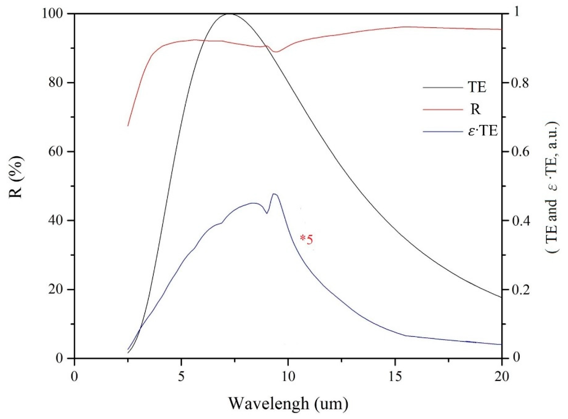
2.3.2. Analysis of Solar Absorption Efficiency, Emissivity, and αs for the SiO2/Cr/SiO2 CSSAs

Reflectance for each film at any one wavelength can be derived from Section 2.3.1. Subsequently, solar absorption efficiency (αs) is calculated by fitting this reflectance data to the spectral power density of the standard AM 1.5 solar spectrum, as referenced in [36].
α s = 0.25 2.0 ( 1 R ( λ ) ) S D ( λ ) d λ 0.25 2.0 S D ( λ ) d λ
where R(λ) and SD(λ) are, respectively, the measured reflectance and the spectral power density of AM1.5 at the wavelength of λ.
Subsequently, emissivity (ε) is calculated by fitting the reflectance data to the spectral power density of the thermal radiation, as referenced in [36].
ε = 2.5 25 ( 1 R ( λ ) ) TE ( λ , T ) d λ 2.5 25 TE ( λ , T ) d λ
PTCE = α s ε ( σ T 4 ) 0 . 25 2.0 S D ( λ ) d λ
where R(λ) and TE(λ) are, respectively, the measured reflectance and the thermal radiation spectral power density at the film’s temperature T and wavelength λ. σT4 is the thermal radiation power at the film’s temperature T. σ is the Stefan–Boltzmann constant (5.67 × 10⁻⁸ W⋅m−2⋅K−4).
The mathematical expression for TE(λ) of a blackbody at a specific wavelength λ and temperature T is given by Planck’s law:
T E λ , T = 2 h c 2 λ 5 1 e h c λ k T 1
where c, h, and k are the speed of light (3 × 10⁸ m/s), Planck’s constant (6.626 × 10⁻³⁴ J∙s), and Boltzman’s constant (1.38 × 10⁻²³ J/K), respectively. T is the absolute temperature in Kelvin. λ is the wavelength in meters.
Dan’s review article [50] on spectrally selective dielectric-metal-dielectric coatings provides a solar spectrum on the Earth’s surface and a temperature-dependent infrared radiation spectrum. When the film is at low temperatures (≤400 K), the intensity of solar energy at the Earth’s surface is significantly greater than the intensity of infrared radiation. When the solar absorption efficiency of a DMD film is greater than 90%, its emissivity is about 6% to 10%. Thus, the film’s infrared radiation intensity is less than 2% of the solar intensity (with a relatively small variation, indicating that the relationship between PTCE and αₛ approximates a linear relationship). For example, the absorption efficiency of all test pieces ranges from 90.5% to 93.2% [36], and their emissivity, as measured by FTIR, varies from 7.1% to 9.1%, with a typical range of 6% to 10%. Consequently, the film’s infrared radiation intensity is approximately 1.5% to 2.5% of the solar intensity at a film temperature of 400 K. In this study, a test piece with designed film thicknesses of 85/4.6/75 nm achieves a calculated αs of 96.3%. Figure 1 illustrates the following: (1) the IR reflectance (R) is greater than 90% across most wavelengths, except between 9.2 and 9.8 microns, where it exceeds 89%; (2) the thermal radiation spectral power density (TE) at 400 K; and (3) the thermal radiation spectral power density (ε·TE) of the test piece (at 5× magnification). This test piece only has a calculated emissivity of 7.5%, which is also in the 6–10% range. Therefore, for calculation convenience, it can be considered as 2%.
Therefore, PTCE can be written approximately as
PTCE ≈ αs − 2%

2.3.3. Analysis of Chromaticity for the SiO2/Cr/SiO2 CSSA

Tristimulus values for a color, characterized by its spectral power distribution I(λ) [40], are determined based on the standard observer as described by the following terms:
X = 380 780 I λ x ¯ λ d λ ,
Y = 380 780 I λ y ¯ λ d λ ,
Z = 380 780 I λ z ¯ λ d λ ,
where x ¯ λ , y ¯ λ , z ¯ λ are the CIE 1931 color-matching functions; I λ = D 65 λ R λ . D65 is CIE Standard Illuminant D65.
The chromaticity of a color can be specified by the two derived parameters x and y as follows:
x = X X + Y + Z ,
y = Y X + Y + Z ,
where x and y are the values obtained by translating the measured optical reflectance spectra to CIE1931 chromaticity coordinates.

3. Results and Discussion

3.1. Big Data Analysis of Optical Thin Film for the SiO2/Cr/SiO2 CSSAs

3.1.1. Simulation Settings and Optimal αs

In the thin film optical simulation for SiO2/Cr/SiO2 CSSAs, the layer thickness parameters are set as follows: the top SiO2 layer ranges from 1 to 200 or 300 nm, with 1 nm intervals; the middle Cr layer from 1 to 15 nm, with 0.2 nm intervals; and the bottom SiO2 layer from 1 to 200 or 300 nm, also with 1 nm intervals. The simulation covers a wavelength range of 300 to 2000 nm. As depicted in Figure 2a, the refractive index (n) and extinction coefficient (k) of both SiO2 and Cr layers are determined using an ellipsometer. The substrates used are Cr/Si wafer, Cr/mirror-like SS304, and Cr/sandblasted SS304. On the substrate, SiO2/Cr/SiO2 layers are deposited.
The film thickness of the SiO2/Cr/SiO2 absorbers is defined as the top layer thickness/Cr layer thickness/bottom layer thickness. The unit of layer thickness is nm. From a total of 2,800,000 combinations, the optimal αs is found in a film with thicknesses of 93 nm (top SiO2 layer), 5 nm (Cr layer), and 76 nm (bottom SiO2 layer) (i.e., 93/5/76), resulting in a maximum αs of 96.5%.

3.1.2. Graphing Colored CCD-αs Diagram in the CIE xy Chromaticity Diagram and Analyzing the Relationship Between αs Value and CCD

In this section, utilizing the software of thin film optical simulation, αs analysis, and chromaticity analysis and setting the αs value greater than 90%, the film’s reflectance spectrum, αs, and chromaticity of CSSAs are determined and thus the relationship between the chromaticity coordinate and αs is studied. This analysis enables mapping the film’s CCD, which is associated with the αs, onto the CIE xy chromaticity diagram. The data points with different αs values are represented by different colors. This process effectively links the optical properties of the optical thin film, as revealed by the simulation, to its colorimetric representation, providing a comprehensive understanding of its chromatic distribution behavior in various simulated CSSAs.
Figure 2b–g present the colored CCD-αs diagram, illustrating the relationship between chromaticity coordinates and αs of CSSAs when the αs is greater than 90%. Figure 2b displays a CCD-αs diagram for a Cr layer thickness ranging from 3 nm (inclusive) to less than 4 nm, denoted as 3–4 nm. The subsequent Figure 2b–g display the CCD-αs diagrams for Cr layer thickness intervals ranging from 3–4 nm to 8–9 nm. From Figure 2b, it can be found that the CCD-αs diagram covers any one chromaticity coordinate. So, the CCD region (CCR) is very wide, including pink, orange, yellow, green, blue, and purple. But its green CCD Area (CCA) is the smallest compared to the other CCAs. Roughly speaking, the αs within the same chromaticity area nearly remains the same. Compared to Figure 2b, Figure 2c also shows a broader CCR, with a notably larger green CCA. At the same αs, it encompasses a broader CCR; for instance, the CCR with αs exceeding 96% spans various hues including pink, orange, yellow, green, blue, and purple. Notably, there is a broader region in the yellow-orange and orange regions. Additionally, across all diagrams from Figure 2b–g, the green CCA is the most expansive in Figure 2c.
Figure 2d illustrates that with an increase in the αs, the chromaticity coordinates region shifts further from the area of white light characterized by high-temperature white light (above 6000 K). But it encompasses the lower-temperature white light (below 4000 K) region. The yellow and orange CCAs are notably broader. Figure 2c,d indicate that the highest αs can exceed 96%. The CCR shape in Figure 2e resembles that in Figure 2d but appears as a smaller version with a reduced CCA. Similarly, Figure 2f also mirrors the reduced version of Figure 2c,d, with an even smaller CCA, and the highest αs is less than 94%. Figure 2d–f collectively show that as αs increases, the chromaticity coordinate region moves from the high-temperature white light region. Figure 2g shows only a small CCR when αs ≥ 90% and the highest αs is less than 92%.
In summary, the distribution of αs and chromaticity varies with the film thickness of the CSSAs, and the αs and chromaticity of definite requirements can be readily obtained from the visualized colored CCD-αs diagrams. Table 1 presents an analysis of the relationship between the αs value and CCD in Figure 2b–g, along with the preparation of test samples.

3.2. Design and Fabrication of Seven CSSAs Utilizing Colored CCD-αs Diagrams: Comprehensive Property Analysis Including Investigation into Oxygen Atom Penetration and Cr Layer Oxidation

3.2.1. Design, Fabrication, and Analysis of Seven SiO2/Cr/SiO2 CSSAs Utilizing CCD-αs Diagrams

Following the comprehensive thin film optical simulations and analyses, at least one film layer will be fabricated for each defined Cr layer thickness interval shown in Table 2, as depicted in Figure 2b–f. In Figure 2g, CCR is notably limited, and the peak αs falls below 92%. Consequently, no film is fabricated within the Cr layer thickness range of 8–9 nm. Particularly for the Cr layer thickness intervals of 4–5 and 5–6 nm, as shown in Figure 2c,d, where the highest αs value exceeds 96% and the areas with αs greater than 90% are larger, two CSSAs in each interval will be fabricated. Furthermore, compared to other figures, Figure 2c is notable for its larger area, with the αs exceeding 96%, where the yellowish-orange region is the most expansive.
These analyses found that the simulation area is set to encompass the yellow and orange areas because the area with a αs of more than 96% is wider. This approach enables a film to offer two key benefits: a golden hue and the highest αs. This simulated film with a thickness of 85/4.6/75 nm can achieve a αs of 96.3% (its PTCE ≥ 94.3%). Figure 3a presents the reflectance spectrum of these simulated and fabricated films, along with a photograph of the fabricated film, which exhibits a dark gold color. The chromaticity coordinates of the fabricated film are located at point (A) in the yellowish-orange region of Figure 2c, with a film thickness of about 84.8/4.7/76.1 nm and a αs of 96.2%. This verifies nearly the same results as that of the thin film optical simulations and analysis. Across all Cr layer thickness intervals, except for the 4–5 nm range, the area for green hue remains notably small. Consequently, a green SSA, as depicted at point (B) in Figure 2c, is designed and fabricated. This film, designed with a thickness of 62/4.8/61 nm and a αs of 91.5% and fabricated with a thickness of about 62.1/4.8/61.5 nm and a αs of 91.3%, exhibits a grass-green color. Its reflected spectrum and a photograph are displayed in Figure 3b.
Next, in Figure 2d, corresponding to a Cr film thickness of 5–6 nm, two CSSAs are designed in orange-pink and blue hues. In Figure 2d, the film thicknesses of the films at points (C) and (D) are designed to be 91/5.4/101 nm and 119/5.8/108 nm, respectively, with their αs values being 94.4% and 92.2%, respectively. These films achieve αs values of 94.5% and 92.1%, respectively. Their reflectance spectra and photos are illustrated in Figure 3c,d. Notably, Figure 3d shows that at wavelengths below 500 nm, reflectance increases with decreasing wavelength, especially in the blue light band where reflectance exceeds 10%, reaching over 35% at 400 nm, thus presenting a bright blue appearance.
In the 6–7 nm Cr film thickness interval, as illustrated in Figure 2e, within the purplish-pink chromaticity region, a film is analyzed and designed with a thickness of 96/6.4/86 nm, achieving an improved αs of 95.1%. The fabricated film, positioned precisely at point (E) in Figure 2e, achieves an excellent αs of 95.2%. The reflectance spectra of both the simulated and fabricated films, alongside the photo of the fabricated film, are presented in Figure 3e.
In the Cr layer thickness range of 7–8 nm, as shown in Figure 2f, the maximum observed αs is below 94%. Therefore, a purple CSSA with a thickness configuration of 95/7.2/88 nm is designed and analyzed, labeled as F, achieving an αs of 93.3%. The fabricated film achieves a αs of 93.1%. The reflectance spectra for both simulated and fabricated films, along with the photo, are presented in Figure 3f. Finally, within the 3–4 nm Cr film thickness range depicted in Figure 2a, the color of the CSSA is designed to be a trendy color (earthy gold). Its chromaticity coordinates are located at point (G) in Figure 2a. This CSSA, with a minimal thickness of 46/3.8/43 nm (very thin first and third layers), still achieves a αs greater than 80%. The αs of the film fabricated according to this specification is 85.6%. The respective reflectance spectra and photos are shown in Figure 3g. This film demonstrates an increase of reflectance from 0% as the wavelength increases within the visible light spectrum (400 to 700 nm), and the reflectance exceeds 12% at 700 nm. And this fabricated film displays an earthy gold color.
Figure 4 displays the SEM cross-sectional image of the CSSA sample fabricated as shown in Figure 3e, illustrating layer thicknesses of approximately 96.3/6.4/86.1 nm. This is very close to the originally designed film thickness.

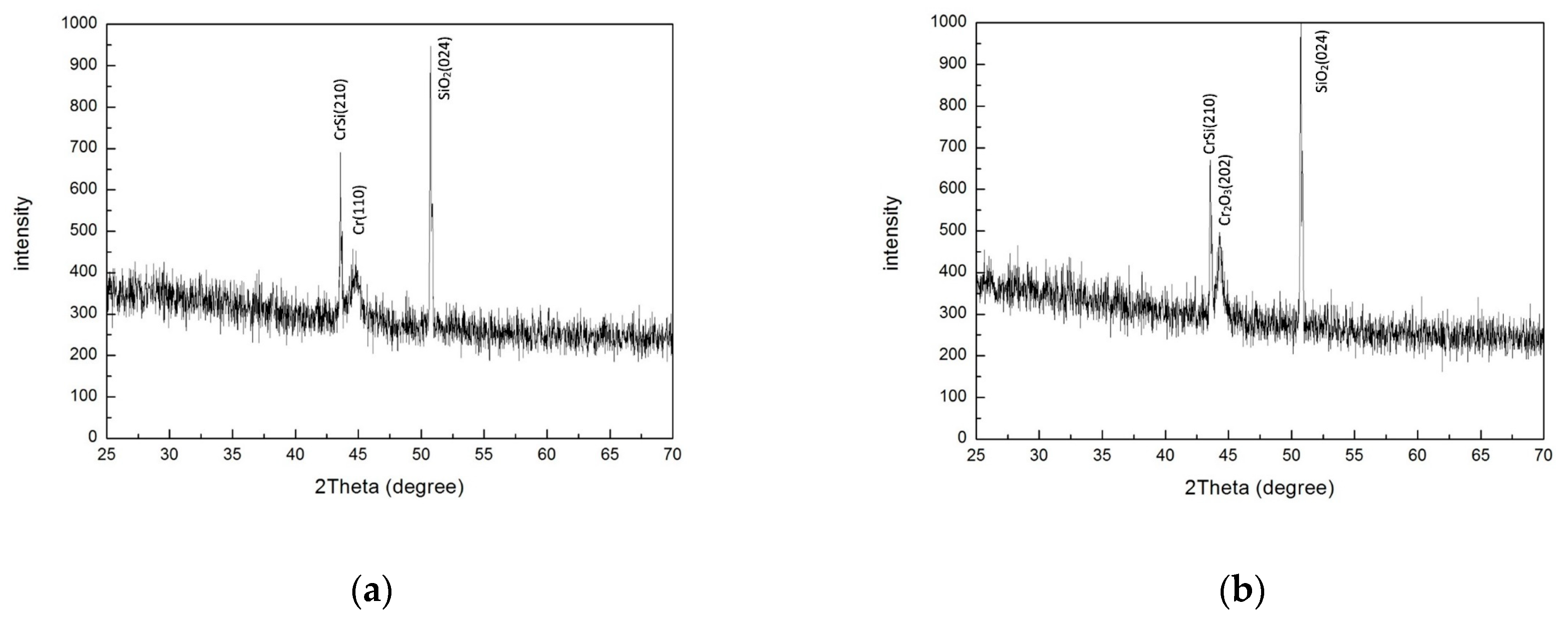
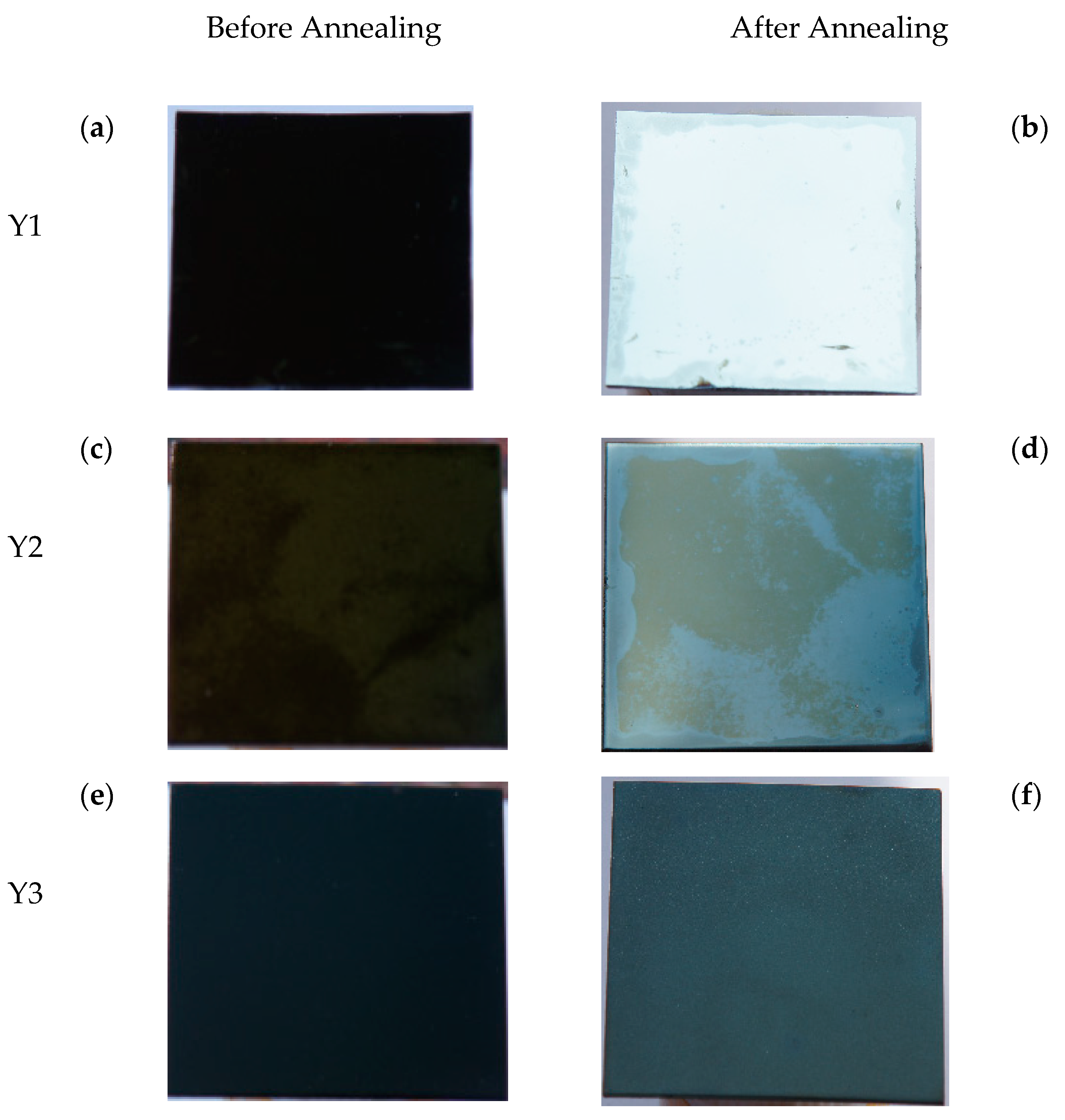
3.2.2. Exploring the Impact of Oxygen Atom Penetration on the Crystallographic Structure of CSSA During Annealing

Figure 5a,b present the XRD patterns illustrating the crystallographic structures of the CSSA before and after annealing, respectively. Before annealing, three distinct diffraction phases are observed: chromium silicide (CrSi) (210) [52], Cr (110), and SiO2 (024). After annealing, these phases transform into CrSi (210), Cr2O3 (202), and SiO2 (024). Notably, even before annealing, the CSSA exhibits a clear crystalline state, especially in the CrSi (210) phase. Driven by the impact of a high-energy ion-assisted source, this CrSi (210) phase results from the diffusion of Si atoms into the Cr layer and their subsequent reaction with Cr. After annealing in an air environment, it is observed that phase transition from Cr to Cr2O3 takes place. However, CrSi does not undergo a transition to chromium silicate (CrSiO). The phenomenon can be elucidated as follows: (1) Oxygen atoms or molecules permeate through the topmost layer of SiO2, subsequently interacting with Cr atoms within the Cr layer to form a compact layer of Cr2O3. (2) Oxygen atoms or molecules are hindered by the dense Cr2O3 layer, preventing further diffusion to the underlying layers, and thus inhibiting the oxidation of CrSi to CrSiO.

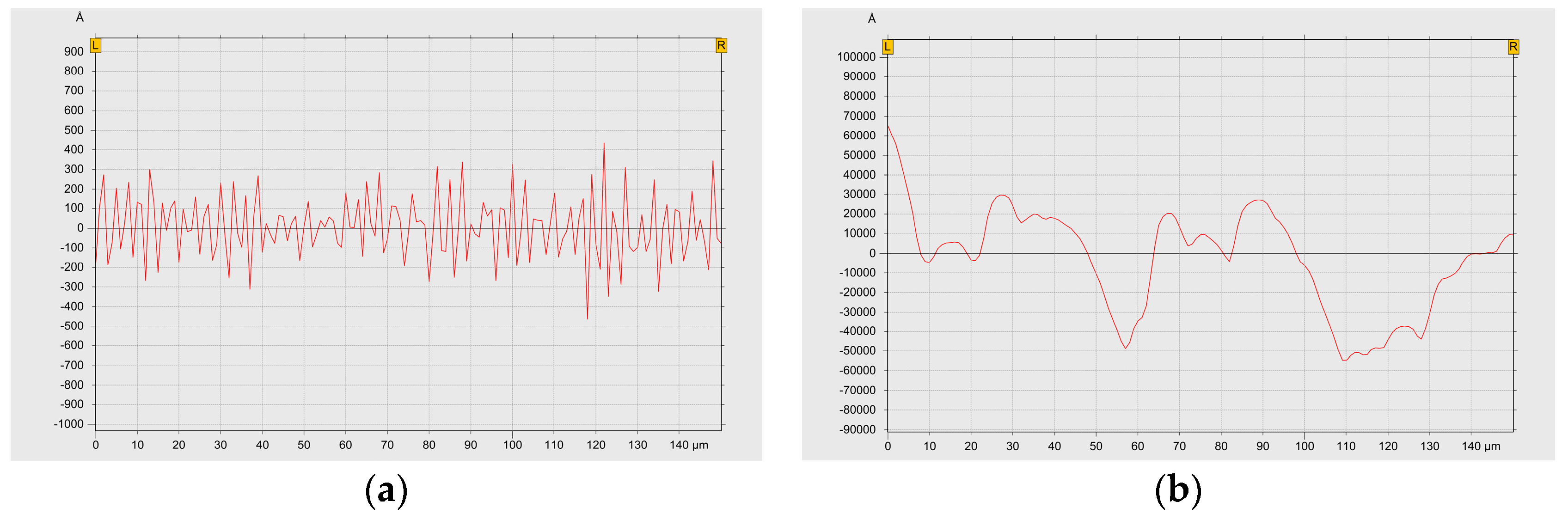
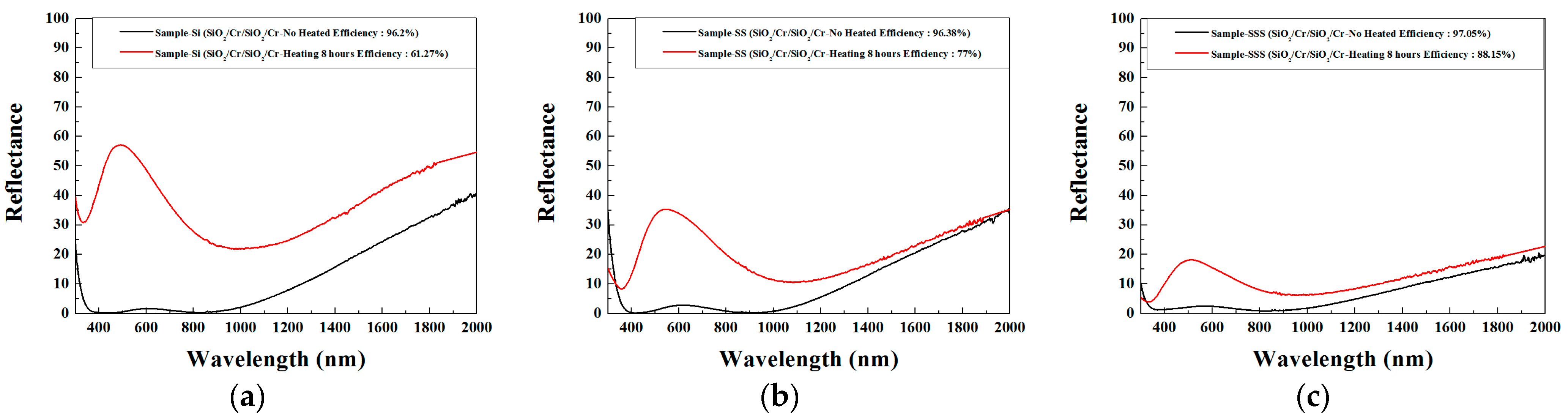
3.3. Effect of the Surface Roughness on Properties of the Fabricated CSSAs

The Si wafers used are of commercial-grade mirror surface quality, with a root mean square surface roughness (Rms) of less than 0.2 nm. The Rms of the mirror-like SS304 stainless steel and sandblasted SS304 stainless steel, measured using a α-stepper and illustrated in Figure 6, are 16 nm and 2642 nm, respectively. Mirror-like SS304 stainless steel is achieved through chemical mechanical planarization and electrolytic polishing. As shown in Figure 6a, there are no deep grooves on the surface of the mirror-like SS304 stainless steel. The sandblasted SS304 stainless steel is obtained by sandblasting the mirror-like SS304 stainless steel. Figure 6b shows that the distance between the grooves on the sandblasted surface is several microns, and the surface is uniformly rough. Cr films exhibit excellent adhesion properties with various substrates, making them a preferred choice for adhesion layers. Therefore, in this study, the absence of deep and narrow grooves on the surfaces of these three substrates allows Cr atoms to easily adhere uniformly, forming a complete and seamless adhesion layer.
SiO2/Cr/SiO2 solar selective absorbers deposited on substrates of Cr/Si wafer, Cr/mirror-like SS304, and Cr/sandblasted SS304 are designated Y1, Y2, and Y3, respectively. Figure 7a–c depict the reflectance spectra of these three CSSAs (Y1, Y2, and Y3) both before and after annealing for 8 h at 450 °C in an air environment. The black line represents the reflectance spectrum of the unannealed specimen, while the red line represents the reflectance spectrum of the annealed specimen. Initially, the αss for Y1, Y2, and Y3 are 96.2%, 96.4%, and 97.1%, respectively, indicating that a rougher surface correlates with a higher αs. The rougher the surface, the more times the incident light will be reflected, resulting in multiple absorptions. Consequently, this leads to a higher αs. However, after annealing, the αss decreased to 61.3%, 77.0%, and 88.2%, respectively, with a lesser reduction in αs observed for rougher surfaces. This may be because a rougher surface increases the film layer’s adhesion, resulting in a denser film that is less susceptible to oxidation. Photographs of Y1, Y2, and Y3, both before and after annealing, are shown in Figure 8a–f. After annealing, Y1’s αs declines from 96.2% to 61.3%, and its color shifts from dark gold to nearly white. The observed color shift is due to significant oxidation of the Cr layer, leading to a reduction in its absorbance. This results in the reflectance within the visible light spectrum surpassing 35% (as indicated by the red line in Figure 7a, giving the film an almost white appearance).
Evans diagrams for three specimens (Y0, Y2, and Y3) in a 1 M NaCl solution are presented in Figure 9. Y0 is an uncoated mirror-like SS304. The values for corrosion potential (ϕcorr), corrosion current density (ⅈcorr), and corrosion rate are summarized in Table 3. SS304 is naturally corrosion-resistant, and both Y2 and Y3 exhibit enhanced corrosion resistance compared to SS304. It is observed that a rougher surface results in a lower corrosion current density and corrosion rate, and a higher corrosion potential, implying that a CSSA on a rougher surface more effectively reduces the material’s electrochemical activity in a corrosive environment.

3.4. Discussion and Explanation

Exploring the properties of films with millions of film thickness variations is impractical through experimental methods. However, using thin film optical simulation and analyses of αs and chromaticity, the distribution of chromaticity coordinates based on αs in the CIE xy chromaticity diagram can be easily explored and analyzed. This approach facilitates comprehension of the effects that variations in film thickness have on its αs and chromaticity, thereby enhancing the exploration and analysis process. The conclusions drawn from Figure 2 are as follows: (1) Chromaticity and αs demonstrate significant variations with changes in film thickness, as observed in Figure 2b–g. (2) Within a specified αs range, such as 94% to 95%, the colored CCD-PTCE diagram depicts the colors and corresponding covered areas. (3) For a specific color requirement such as green, despite its smaller area, it can still determine the maximum attainable αs and the corresponding film thickness. (4) For a desired color such as yellow-orange and a αs exceeding 96%, the diagram illustrates the broadest area at Cr layer thicknesses ranging from 4 to 5 nm. Thus, akin to Figure 2, the colored CCD-αs diagram facilitates the estimation of film thickness for specific αs and color requirements.
The film thickness includes the thicknesses of the top layer, Cr layer, and bottom layer. Using software that includes thin film optical simulation and analysis tools for αs and chromaticity, the αs and chromaticity can be determined. The colored CCD-αs diagram, as depicted in Figure 2, is constructed to visually demonstrate the relationship between the film’s chromaticity coordinates and αs. Using this diagram to design required CSSAs, firstly, the appropriate αs and chromaticity coordinate region from Figure 2 are selected, followed by analyzing the film thickness to obtain a simulated film. Based on this approach, seven films are designed, chosen, and fabricated. Seven selected films are distributed across various colors and exhibit different αs values. The optical properties of these fabricated films are consistent with the results obtained from the initial simulations and designs.
The specimens shown in Figure 3e, Figure 4, Figure 5, Figure 7a and Figure 8a are SiO2/Cr/SiO2 CSSAs deposited on Cr/Si wafer substrates. Influenced by a high-energy ion-assisted source, the unannealed CSSA exhibits a clear crystalline structure, especially in the CrSi (210) phase. The substrate transitions from a wafer substrate of Cr/Si to CrSi/Si. After annealing, the αs of Y1 declines from 96.2% to 61.3%, with its color transitioning from dark gold to nearly white, as depicted in Figure 8a,b. As shown in Figure 5 and Figure 7a, the αs decrease during annealing is attributed to the phase transformation from Cr to Cr2O3, indicating the oxidation of Cr to Cr2O3. However, CrSi does not oxidize to CrSiO, possibly because the oxidation of Cr in the Cr layer to dense Cr2O3 obstructs the passage of oxygen atoms or molecules. Inference suggests that oxygen atoms or molecules can initially oxidize the inner chromium layer through tiny pinholes in the surface layer in a vertical direction, followed by horizontal diffusion and continued oxidation within the layer.
It is observed that a rougher surface results in a smaller reduction in αs, suggesting that a rougher surface mitigates the oxidation of the chromium layer in the CSSA. This could be due to the presence of tiny pinholes in the top SiO2 layer facilitating Cr oxidation. At the same time, the rough surface’s undulations impede the continuous horizontal oxidation of oxygen atoms or molecules within the Cr layer. Pronounced surface undulations serve as a barrier to this horizontal oxidation.
The Evans diagrams also demonstrate that the rougher the surface, the greater the reduction in electrochemical activity.
Hence, a CSSA on a rougher surface exhibits higher αs, antioxidant, and anti-corrosion properties, thereby enhancing its overall performance.
The SiO2/Cr/SiO2 CSSA has a high PTCE of over 90%, reaching up to 94.5%, with a full range of color options and excellent weather resistance, making it ideal for any type of architectural application.

4. Conclusions

Thin film optical simulation plays a crucial role in optical thin film coating technology. However, there is currently a lack of literature providing simple and clear diagrams to analyze and visualize CSSA optical properties, specifically regarding the thickness of each layer to meet chromaticity and high αs requirements. This study effectively explores and analyzes the impact of different film thicknesses on αs and chromaticity, as demonstrated in the CIE xy diagram. A series of colored CCD-αs diagrams were constructed and analyzed, revealing a broad color distribution for CSSAs with αs exceeding 90%, encompassing all colors. Subsequently, leveraging the colored CCD-αs diagrams, seven SiO2/Cr/SiO2 CSSAs were meticulously designed, fabricated, and subjected to optical and material property analysis. A film achieving an optimal αs exceeding 96% and exhibiting a yellow-orange hue was successfully engineered, aligning with initial design expectations. The techniques and methodologies employed in this study enhance the precision and convenience of both research and manufacturing. They equip users, spanning from researchers to industrial design and production engineers, with a comprehensive set of tools for investigating and producing Colored Solar Selective Absorbers.
Moreover, this study analyzes the impact of oxygen atoms or molecules infiltrating CSSAs, leading to Cr layer oxidation and subsequent alterations in CSSA performance. Additionally, the effect of surface roughness on CSSAs is examined, revealing that rougher surfaces enhance αs, oxidation resistance, and corrosion resistance.

Author Contributions

Conceptualization, F.-D.L.; Methodology, Y.-T.L.; Software, Y.-T.L.; Validation, F.-D.L. and C.-S.C.; Formal analysis, Y.-T.L.; Investigation, C.-S.C.; Data curation, Y.-T.L.; Writing—original draft, F.-D.L.; Writing—review & editing, F.-D.L.; Funding acquisition, F.-D.L. All authors have read and agreed to the published version of the manuscript.

Funding

This work is supported by National Science Council in Taiwan under Contract No. MOST 109-2637-E-992-004.

Institutional Review Board Statement

Not applicable.

Informed Consent Statement

Not applicable.

Data Availability Statement

The original contributions presented in the study are included in the article, further inquiries can be directed to the corresponding authors.

Acknowledgments

We extend our gratitude to Prof. Dr. Yu-Lin, Joseph, Kuo from the Department of Mechanical Engineering at Taiwan University of Science and Technology for his assistance with the measurement of the material’s electrochemical behavior.

Conflicts of Interest

The authors declare no conflict of interest.

References

  1. Lai, F.D. Effect of each layer thickness in Al2O3/Pt/Al2O3 solar absorber films on the photo-thermal conversion efficiency for rapid industrial production. Surf. Coat. Technol. 2020, 389, 125503. [Google Scholar] [CrossRef]
  2. Conserval Systems, Inc. Solar Wall. Available online: https://pdf.archiexpo.com/pdf/conserval-engineering/solarwall/60659-230117.html (accessed on 1 September 2024).
  3. Extended Campuses Building Expansion. Available online: https://in.nau.edu/facility-services/pdc/building-green/extended-campuses-building/ (accessed on 1 September 2024).
  4. Natural Ventilation System/Solar Chimney. Department of Environmental Engineering, Kitakyushu University, Japan. Available online: https://www.ibec.or.jp/jsbd/G/features.htm (accessed on 1 September 2024).
  5. Zeng, X.; Pelenovich, V.; Neena, D.; Xu, C.; Zhang, X.; Pogrebnjak, A.; Yang, B.; Liu, S. Thermal stability of high entropy graded solar selective absorbers deposited by non-equilibrium RF magnetron sputtering. J. Alloys Compd. 2023, 944, 169248. [Google Scholar] [CrossRef]
  6. Pelenovich, V.; Zeng, X.; Liu, Y.; Zhang, X.; Liu, H.; Pogrebnjak, A.; Vildanov, R.; Yang, B.; Liu, S. AlCrO protected textured stainless-steel surface for high temperature solar selective absorber applications. Surf. Coat. Technol. 2022, 436, 128282. [Google Scholar] [CrossRef]
  7. Liu, H.D.; Yang, B.; Mao, M.R.; Liu, Y.; Chen, Y.M.; Cai, Y.; Hu, X.J. Enhanced thermal stability of solar selective absorber based on nano-multilayered TiAlON films deposited by cathodic arc evaporation. Appl. Surf. Sci. 2020, 501, 501144025. [Google Scholar] [CrossRef]
  8. Qiu, X.-L.; Gao, X.-H.; He, C.-Y.; Chen, B.-H.; Liu, G. Structure, optical simulation and thermal stability of the HfB2-based high-temperature solar selective absorbing coatings. RSC Adv. 2019, 9, 29726–29733. [Google Scholar] [CrossRef]
  9. Yang, Y.; Wang, T.; Yao, T.; Li, G.; Sun, Y.; Cao, X.; Ma, L.; Peng, S. Preparation of a novel TiN/TiNxOy/SiO2 composite ceramic films on aluminum substrate as a solar selective absorber by magnetron sputtering. J. Alloys Compd. 2020, 815, 152209. [Google Scholar] [CrossRef]
  10. Lai, F.D.; Yan, Y.S. Optical properties, contour map and fabrication of Al2O3/Pt/Al2O3/Ta multilayer films for solar selective absorptance layer. Sci. Adv. Mater. 2019, 11, 1106–1111. [Google Scholar] [CrossRef]
  11. Nuru, Z.Y.; Arendse, C.J.; Khamlich, S.; Kotsedi, L.; Maaza, M. Tantalum diffusion barrier layer to improve the thermal stability of AlxOy/Pt/AlxOy multilayer solar absorber. Sol. Energy 2014, 107, 89–96. [Google Scholar] [CrossRef]
  12. Nuru, Z.Y.; Arendse, C.J.; Khamlich, S.; Maaza, M. Optimization of AlxOy/Pt/AlxOy multilayer spectrally selective coatings for solar thermal applications. Vacuum 2012, 86, 2129–2135. [Google Scholar] [CrossRef]
  13. Wang, S.; Chen, F.; Lu, W. Advanced thin film photo-thermal materials and applications. Adv. Thermoelec. Mater. 2019, 8, 317–381. [Google Scholar]
  14. Lai, F.-D.; Li, W.-Y.; Chang, K.-C.; Wang, Y.-Z.; Chi, P.-L.; Su, J.-Y. Optical properties, optimized design and fabrication of SiO2/W/SiO2 films for solar selective absorber. Integr. Ferroelectr. 2012, 137, 77–84. [Google Scholar] [CrossRef]
  15. Lai, F.D.; Li, W.Y. SiO2/Ti/SiO2 Three-layer films used as solar selective absorber layer in heat energy collector. Integr. Ferroelec. 2013, 145, 158–164. [Google Scholar] [CrossRef]
  16. Shaffei, M.F.; Hussein, H.S.; Abouelata, A.M.A.; Osman, R.M.; Mohammed, M.S. Effect of sealing on characteristics of nano-porous aluminum oxide as black selective coatings. Clean. Eng. Technol. 2021, 4, 100156. [Google Scholar] [CrossRef]
  17. Wu, Z.; Ren, Z.; Wang, J.; Hou, S.; Liu, Y.; Zhang, Q.; Mao, J.; Liu, X.; Cao, F. Realization of an efficient wide-angle solar selective absorber via the impedance matching. Sol. Energy Mater. Sol. Cells 2022, 238, 111582. [Google Scholar] [CrossRef]
  18. Wang, X.; Yuan, X.; Gong, D.; Cheng, X.; Li, K. Optical properties and thermal stability of AlCrON based multilayer solar selective absorbing coating for high temperature applications. J. Mater. Res. Technol. 2021, 15, 6162–6174. [Google Scholar] [CrossRef]
  19. Tian, Y.; Liu, X.; Ghanekar, A.; Zheng, Y. Scalable-manufactured metal–insulator–metal based selective solar absorbers with excellent high-temperature insensitivity. Appl. Energy 2021, 281, 116055. [Google Scholar] [CrossRef]
  20. Guo, H.-X.; Yu, D.-M.; He, C.-Y.; Qiu, X.-L.; Zhao, S.-S.; Liu, G.; Gao, X.-H. Double-layer solar absorber coating based on high entropy ceramic AlCrMoTaTiN: Structure, optical properties and failure mechanism. Surf. Interfaces 2021, 24, 101062. [Google Scholar] [CrossRef]
  21. He, C.-Y.; Gao, X.-H.; Yu, D.-M.; Guo, H.-X.; Zhao, S.-S.; Liu, G. Highly enhanced thermal robustness and photothermal conversion efficiency of solar-selective absorbers enabled by high-entropy alloy nitride MoTaTiCrN nanofilms. ACS Appl. Mater. Interfaces 2021, 13, 16987–16996. [Google Scholar] [CrossRef]
  22. Liu, H.; Xie, M.; Ai, Q.; Yu, Z. Ultra-broadband selective absorber for near-perfect harvesting of solar energy. J. Quant. Spectrosc. Radiat. Transfer. 2021, 266, 107575. [Google Scholar] [CrossRef]
  23. Liu, B.; Wang, C.; Bazri, S.; Badruddin, I.A.; Orooji, Y.; Saeidi, S.; Wongwises, S.; Mahian, O. Optical properties and thermal stability evaluation of solar absorbers enhanced by nanostructured selective coating films. Powder Technol. 2021, 377, 939–957. [Google Scholar] [CrossRef]
  24. Tian, Y.; Liu, X.; Caratenuto, A.; Li, J.; Zhou, S.; Ran, R.; Chen, F.; Wang, Z.; Wan, K.-T.; Xiao, G.; et al. A new strategy towards spectral selectivity: Selective leaching alloy to achieve selective plasmonic solar absorption and infrared suppression. Nano Energy 2022, 92, 106717. [Google Scholar] [CrossRef]
  25. Zhang, J.; Wang, C.; Shi, J.; Wei, D.; Zhao, H.; Ma, C. Solar selective absorber for emerging sustainable applications. Adv. Energy Sustain. Res. 2022, 3, 2100195. [Google Scholar] [CrossRef]
  26. Niranjan, K.; Kondaiah, P.; Biswas, A.; Kumar, V.; Srinivas, G.; Barshilia, H. Spectrally selective solar absorber coating of W/WAlSiN/SiON/SiO2 with enhanced absorption through gradation of optical constants: Validation by simulation. Coatings 2021, 11, 334. [Google Scholar] [CrossRef]
  27. Wang, Z.-Y.; Hu, E.-T.; Cai, Q.-Y.; Wang, J.; Tu, H.-T.; Yu, K.-H.; Chen, L.-Y.; Wei, W. Accurate design of solar selective absorber based on measured optical constants of nano-thin Cr Film. Coatings 2020, 10, 938. [Google Scholar] [CrossRef]
  28. Ji, S.-M.; Oh, S.-W.; Yoon, T.-H. Smart window based on angular-selective absorption of solar radiation with guest–host liquid crystals. Crystals 2021, 11, 131. [Google Scholar] [CrossRef]
  29. El-Fattah, H.A.A.; El-Mahallawi, I.S.; Shazly, M.H.; Khalifa, W.A. Optical properties and microstructure of TiNxOy and TiN thin films before and after annealing at different conditions. Coatings 2019, 9, 22. [Google Scholar] [CrossRef]
  30. Tyagi, P.K.; Kumar, R.; Said, Z. Recent advances on the role of nanomaterials for improving the performance of photovoltaic thermal systems: Trends, challenges and prospective. Nano Energy 2022, 93, 106834. [Google Scholar] [CrossRef]
  31. Said, Z.; Sundar, L.S.; Tiwari, A.K.; Ali, H.M.; Sheikholeslami, M.; Bellos, E.; Babar, H. Recent advances on the fundamental physical phenomena behind stability, dynamic motion, thermophysical properties, heat transport, applications, and challenges of nanofluids. Phys. Rep. 2022, 946, 1–94. [Google Scholar] [CrossRef]
  32. Anderson, T.; Duke, M.; Carson, J. The effect of colour on the thermal performance of building integrated solar collectors. Sol. Energy Mater. Sol. Cells 2010, 94, 350–354. [Google Scholar] [CrossRef]
  33. Selvakumar, N.; Karthik, G.; Jayaraj, S.; Barshilia, H.C. Sprayable PEDOT:PSS based spectrally selective coating for solar energy harvesting. Sol. Energy Mater. Sol. Cells 2021, 221, 110906. [Google Scholar] [CrossRef]
  34. Xuan, Z.; Li, J.; Liu, Q.; Yi, F.; Wang, S.; Lu, W. Artificial structural colors and applications. Innovation 2021, 2, 100081. [Google Scholar] [CrossRef] [PubMed]
  35. Guo, H.-X.; He, C.-Y.; Qiu, X.-L.; Shen, Y.-Q.; Liu, G.; Gao, X.-H. A novel multilayer high temperature colored solar absorber coating based on high-entropy alloy MoNbHfZrTi: Optimized preparation and chromaticity investigation. Sol. Energy Mater. Sol. Cells 2020, 209, 110444. [Google Scholar] [CrossRef]
  36. Lai, F.D.; Li, W.Y. Design, fabrication and analysis for Al2O3/Ti/Al2O3 colored solar selective absorbers for building applications. Coatings 2022, 12, 521. [Google Scholar] [CrossRef]
  37. Yang, R.; Liu, J.; Lin, L.; Qu, Y.; Zheng, W.; Lai, F. Optical properties and thermal stability of colored solar selective absorbing coatings with double-layer antireflection coatings. Sol. Energy 2016, 125, 453–459. [Google Scholar] [CrossRef]
  38. Chen, F.; Wang, S.-W.; Liu, X.; Ji, R.; Li, Z.; Chen, X.; Chen, Y.; Lu, W. Colorful solar selective absorber integrated with different colored units. Opt. Express 2017, 24, A92–A103. [Google Scholar] [CrossRef]
  39. Chen, F.; Wang, S.-W.; Liu, X.; Ji, R.; Yu, L.; Chen, X.; Lu, W. High performance colored selective absorbers for architecturally integrated solar applications. J. Mater. Chem. A 2015, 3, 7353–7360. [Google Scholar] [CrossRef]
  40. Wang, C.; Shi, J.; Geng, Z.; Ling, X. Polychromic Al–AlN cermet solar absorber coating with high absorption efficiency and excellent durability, Sol. Energy Mater. Sol. Cells 2016, 144, 14–22. [Google Scholar] [CrossRef]
  41. Dan, A.; Chattopadhyay, K.; Barshilia, H.C.; Basu, B. Colored selective absorber coating with excellent durability. Thin Solid Films 2016, 620, 17–22. [Google Scholar] [CrossRef]
  42. Schuler, A.; Boudaden, J.; Oelhafen, P.; De Chambrier, E.; Roecker, C.; Scartezzini, J.-L. Thin film multilayer design types for colored glazed thermal solar collectors. Sol. Energy Mater. Sol. Cells 2005, 89, 219–231. [Google Scholar] [CrossRef]
  43. Schüler, A.; Roecker, C.; Boudaden, J.; Oelhafen, P.; Scartezzini, J.-L. Potential of quarter-wave interference stacks for colored thermal solar collectors. Sol. Energy 2005, 79, 122–130. [Google Scholar] [CrossRef]
  44. No, L.; Šest, E.; Kapun, G.; Ruiz-Zepeda, F.; Binyamin, Y.; Merzel, F.; Jerman, I. High-solar-absorptance CSP coating characterization and reliability testing with isothermal and cyclic loads for service-life prediction. Energy Environ. Sci. 2019, 12, 1679–1694. [Google Scholar]
  45. Lai, F.D. Optical property analysis, contour map and fabrication of SiO2/Cr/SiO2/Cr multilayer films for high photo-thermal conversion efficiency. Integr. Ferroelectr. 2020, 210, 64–72. [Google Scholar] [CrossRef]
  46. Chang, S.-H.; Lin, S.-S.; Huang, K.-T. Effect of CrSi/CrSi2 content on the microstructure and properties of vacuum hot-pressed Cr-50 wt% Si alloys. Vacuum 2019, 162, 54–62. [Google Scholar] [CrossRef]
  47. Bhushan, T.; Chandrashekhar, A.; Prasat, S.V.; Reddy, I.R. Effect of substrate surface roughness on adhesion of titanium nitride coatings deposited by physical vapour deposition technique. Mater. Sci. Eng. 2020, 981, 042022. [Google Scholar] [CrossRef]
  48. Xiao, W.; Deng, H.; Zou, S.; Ren, Y.; Tang, D.; Lei, M.; Xiao, C.; Zhou, X.; Chen, Y. Effect of roughness of substrate and sputtering power on the properties of TiN coatings deposited by magnetron sputtering for ATF. J. Nucl. Mater. 2018, 509, 542–549. [Google Scholar] [CrossRef]
  49. Lee, L.C.; Ho, W.Y.; Lai, F.D. Effect of substrate surface roughness on the characteristics of CrN hard film. Mater. Chem. Phys. 1996, 43, 266–273. [Google Scholar] [CrossRef]
  50. Dan, A.; Barshili, H.C.; Chattopadhyay, K.; Basu, B. Solar energy absorption mediated by surface plasma polaritons in spectrally selective dielectric-metal-dielectric coatings: A critical review. Renew. Sustain. Energy Rev. 2017, 79, 1050–1077. [Google Scholar] [CrossRef]
  51. Cho, S.-H.; Seo, M.-K.; Kang, J.-H.; Yang, J.-K.; Kang, S.-Y.; Lee, Y.-H.; Hwang, K.H.; Lee, B.D.; Lee, J.-G.; Song, Y.-W.; et al. A Black Metal-dielectric Thin Film for High-contrast Displays. J. Korean Phys. Soc. 2009, 55, 501–507. [Google Scholar] [CrossRef]
  52. Caia, H.; Tonga, D.; Wanga, Y.; Songa, X.; Ding, B. Reactive synthesis of porous Cu3Si compound. J. Alloys Compd. 2011, 509, 1672–1676. [Google Scholar] [CrossRef]
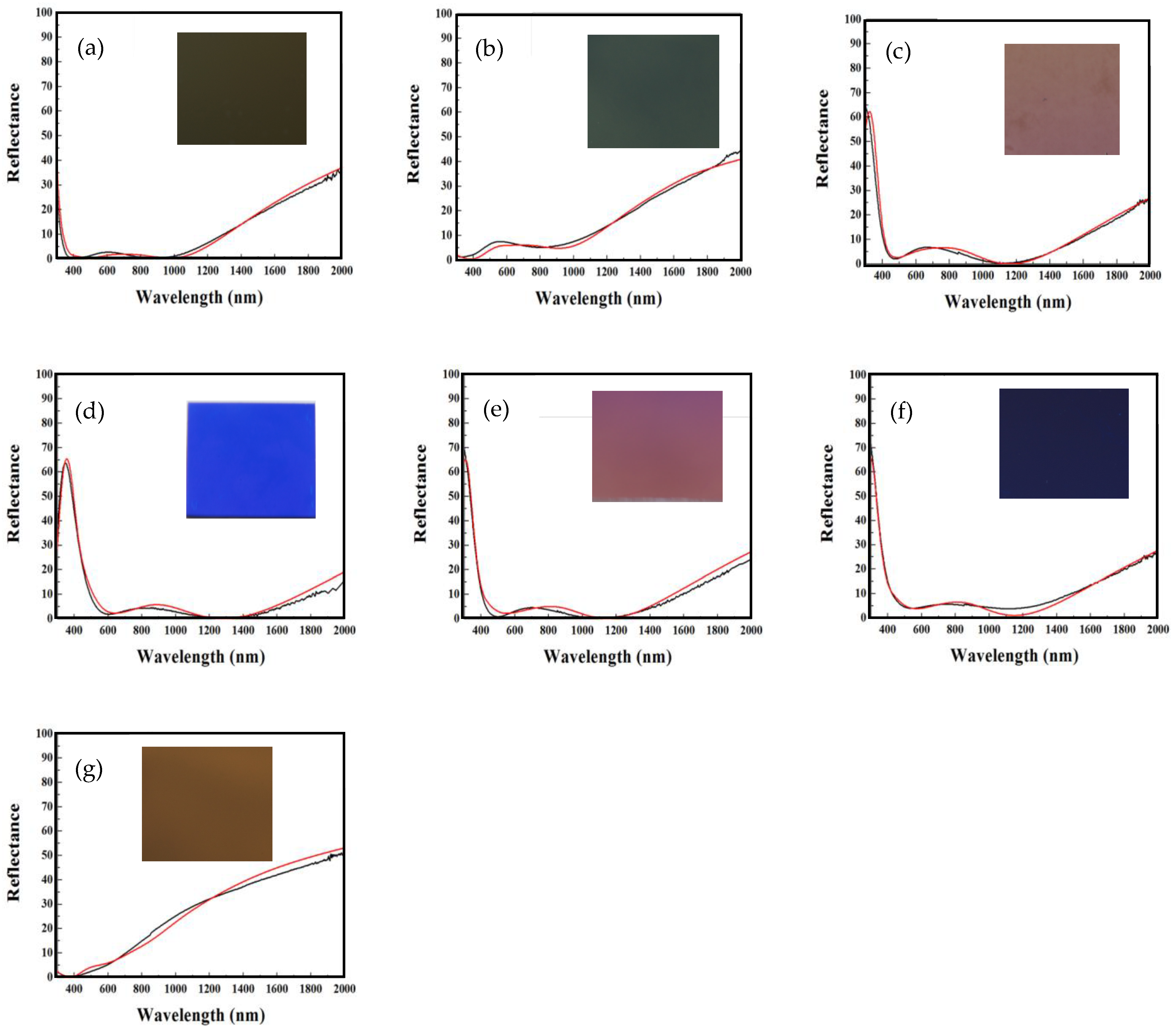
Figure 1. The IR reflectance (R), the thermal radiation spectral power density (TE), and the thermal radiation spectral power density (ε⋅TE) of the test piece (at 5× magnification) at 400 K.
Materials 17 05810 g001
Figure 2. (a) The refractive index (n) and extinction coefficient (k) of both SiO2 and Cr layers and the CCD-αs diagrams for the Cr layer thickness intervals ranging (b) 3–4, (c) 4–5, (d) 5–6, (e) 6–7, (f) 7–8, and (g) 8–9 nm. A to G are the designed and fabricated films. The colored CCD-αs diagrams illustrate the relationship between chromaticity coordinates and αs of CSSAs when the αs is greater than 90%.
Materials 17 05810 g002
Figure 3. The reflected spectrum and photograph of the fabricated CSSAs for the layer thicknesses of (a) 85/4.8/76, (b) 62/4.8/61, (c) 90/5.2/101, (d) 119/5.8/108, (e) 97/6.2/86, (f) 95/7.2/88, and (g) 45/3.8/41 nm. The red and black lines are simulated and measured reflectance spectra of the designed film, respectively. The red and black lines are simulated and measured reflectance spectra of the designed film, respectively.
Materials 17 05810 g003
Figure 4. An SEM cross-sectional image of the CSSA.
Materials 17 05810 g004
Figure 5. The XRD patterns, which depict the crystallographic structures of the CSSA (a) before and (b) after annealing.
Materials 17 05810 g005
Figure 6. The RMS surface roughness of (a) the mirror-like SS304 and (b) sandblasted SS304.
Materials 17 05810 g006
Figure 7. The reflectance spectra of the three CSSAs ((a) Y1, (b) Y2, and (c) Y3) both before and after annealing. The red and black lines are the reflectance spectra of these three CSSAs before and after annealing, respectively.
Materials 17 05810 g007
Figure 8. Photographs of Y1, Y2, and Y3, both before and after annealing.
Materials 17 05810 g008
Figure 9. Evans diagrams for the three CSSAs (Y0, Y2, and Y3) in a 1 M NaCl solution.
Materials 17 05810 g009
Table 1. Analyzing the relationship between αs value and CCD, and preparing the test pieces.
Figure
Number
Thickness Range (X) of a Cr Layer (nm)Chromaticity
Coordinate
Distribution Region
αs Range
(%)
Explanation of Chromaticity Coordinate Distribution and Preparation of Test Pieces
Figure 2b3 ≤ X < 4All Colors *90 to 95Its green CCD Area (CCA) is the smallest compared to other CCAs. Roughly speaking, αs within the same chromaticity area nearly remains the same. (Prepare a test piece of G).
Figure 2c4 ≤ X < 5All Colors90 to 97The CCA with αs exceeding 96% spans various hues including all colors. Notably, there is a broader region in the yellow-orange and orange regions. (Prepare a test piece of A).
Across all diagrams from Figure 2b–g, the green CCA is most expansive in Figure 2c. (Prepare a test piece of B).
Figure 2d5 ≤ X < 6All Colors90 to 97With an increase in the αs, the chromaticity coordinate region shifts further from the white light region. The yellow and orange CCAs are notably broader. (Prepare two test pieces, C and D).
Figure 2e6 ≤ X < 7All Colors90 to 96The CCR shape in Figure 2e resembles that in Figure 2d but appears as a smaller version with a reduced CCA. (Prepare a test piece of E).
Figure 2f7 ≤ X < 8pink, orange, blue, and purple90 to 94Figure 2f also mirrors the reduced version of Figure 2c,d, with an even smaller CCA, and the highest αs is less than 94%. (Prepare a test piece of F).
Figure 2g8 ≤ X < 9pink, blue, and purple90 to 92There is only a small CCR when αs ≥ 90% and the highest αs is less than 92%.
* “All colors” means complete coverage of the entire color gamut, including pink, orange, yellow, green, blue, and purple.
Table 2. Film thickness, PTCE, and color for designed and fabricated CSSAs.
Test Piece EncodingIn
Figure
Designed
Film Thickness
(nm)
Reflectance Spectrum of Test Piece (Figure)Calculated
αs (%)
Measured
αs (%)
Color
AFigure 2b85/4.6/75Figure 3a96.396.2dark gold
BFigure 2b62/4.8/61Figure 3b91.591.3grass-green
CFigure 2c91/5.4/101Figure 3c94.494.5orange-pink
DFigure 2c119/5.8/108Figure 3d92.292.1bright blue
EFigure 2d96/6.4/86Figure 3e95.195.2purplish-pink
FFigure 2e95/7.2/88Figure 3f93.393.1purple
GFigure 2a46/3.8/43Figure 3g86.885.6earthy gold
Table 3. Potentiodynamic scan for mirror-like SS304, CSSA/Cr/mirror-like SS304, and CSSA/Cr/ Cr/sandblasted SS304 specimens in 1 M NaCl solution.
ϕcorr
(mV)
corr
(μA/cm2)
Corrosion Rate
(×10−3 mmpy)
Y0−445.160.584.398
Y2−161.12 0.332.539
Y3−4.650.241.812
Disclaimer/Publisher’s Note: The statements, opinions and data contained in all publications are solely those of the individual author(s) and contributor(s) and not of MDPI and/or the editor(s). MDPI and/or the editor(s) disclaim responsibility for any injury to people or property resulting from any ideas, methods, instructions or products referred to in the content.

