
Optoelectronic Properties of Cold Plasma-Deposited, Oxidized Sn–C Thin Films


Abstract
1. Introduction
2. Materials and Methods
3. Results
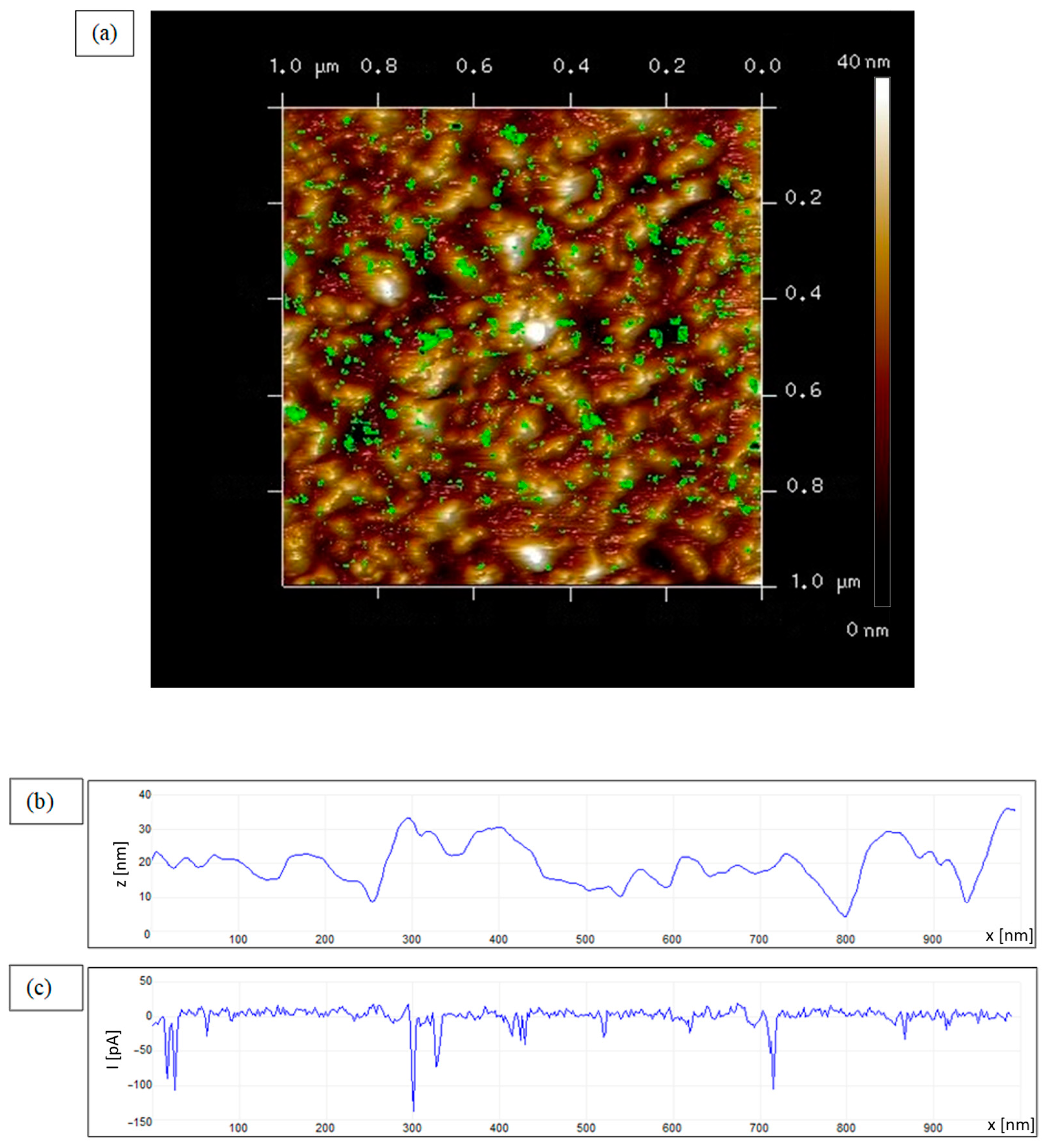
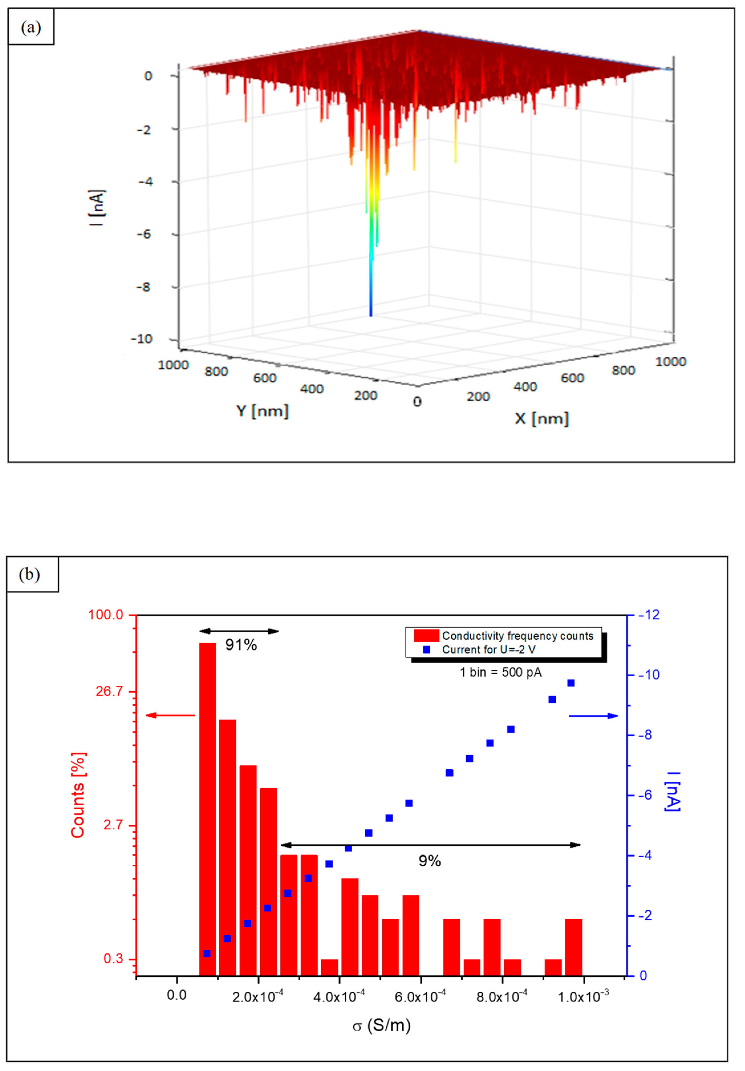
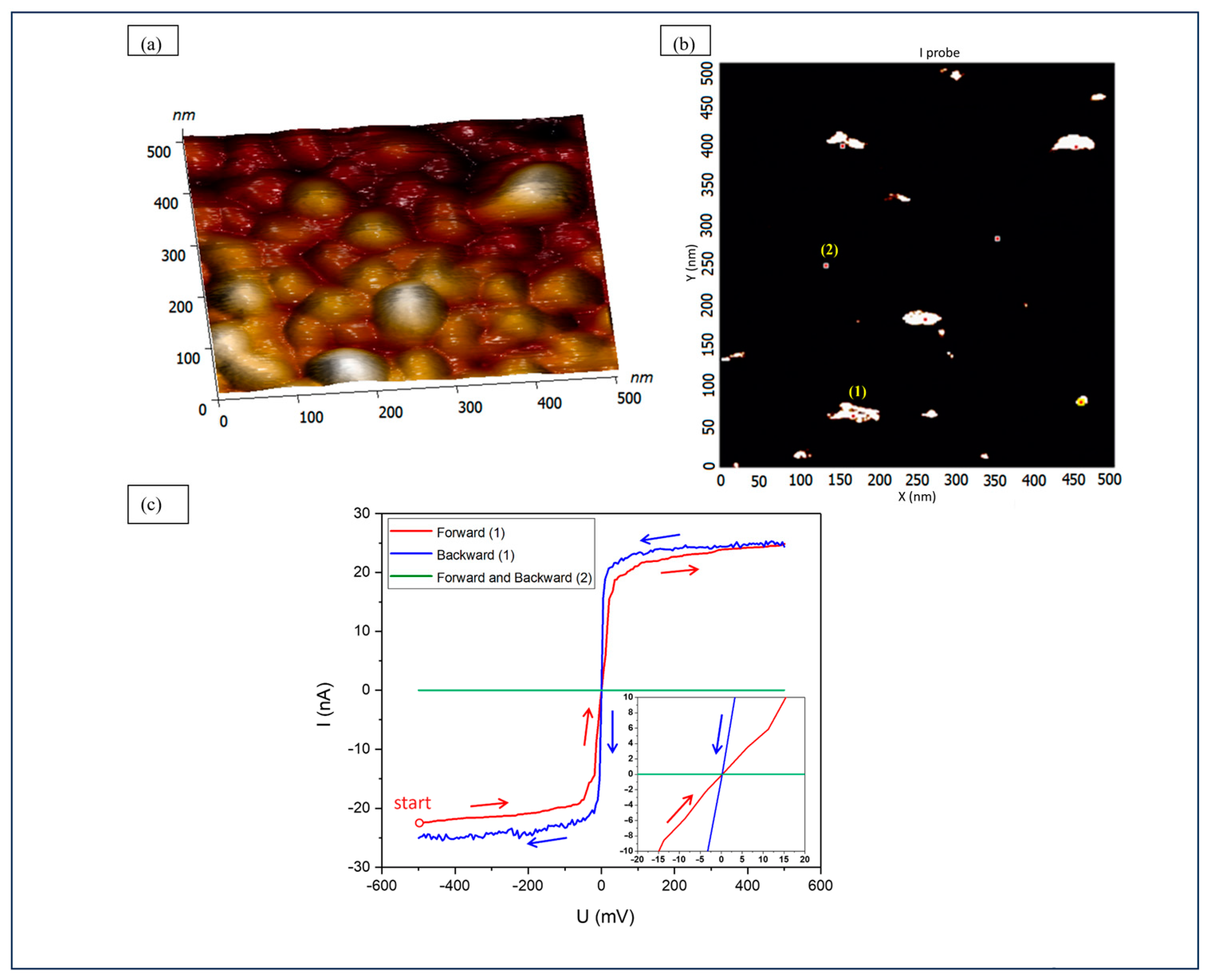
3.1. Nanoconductivity
3.2. Local Conductivity
3.3. Macroconductivity
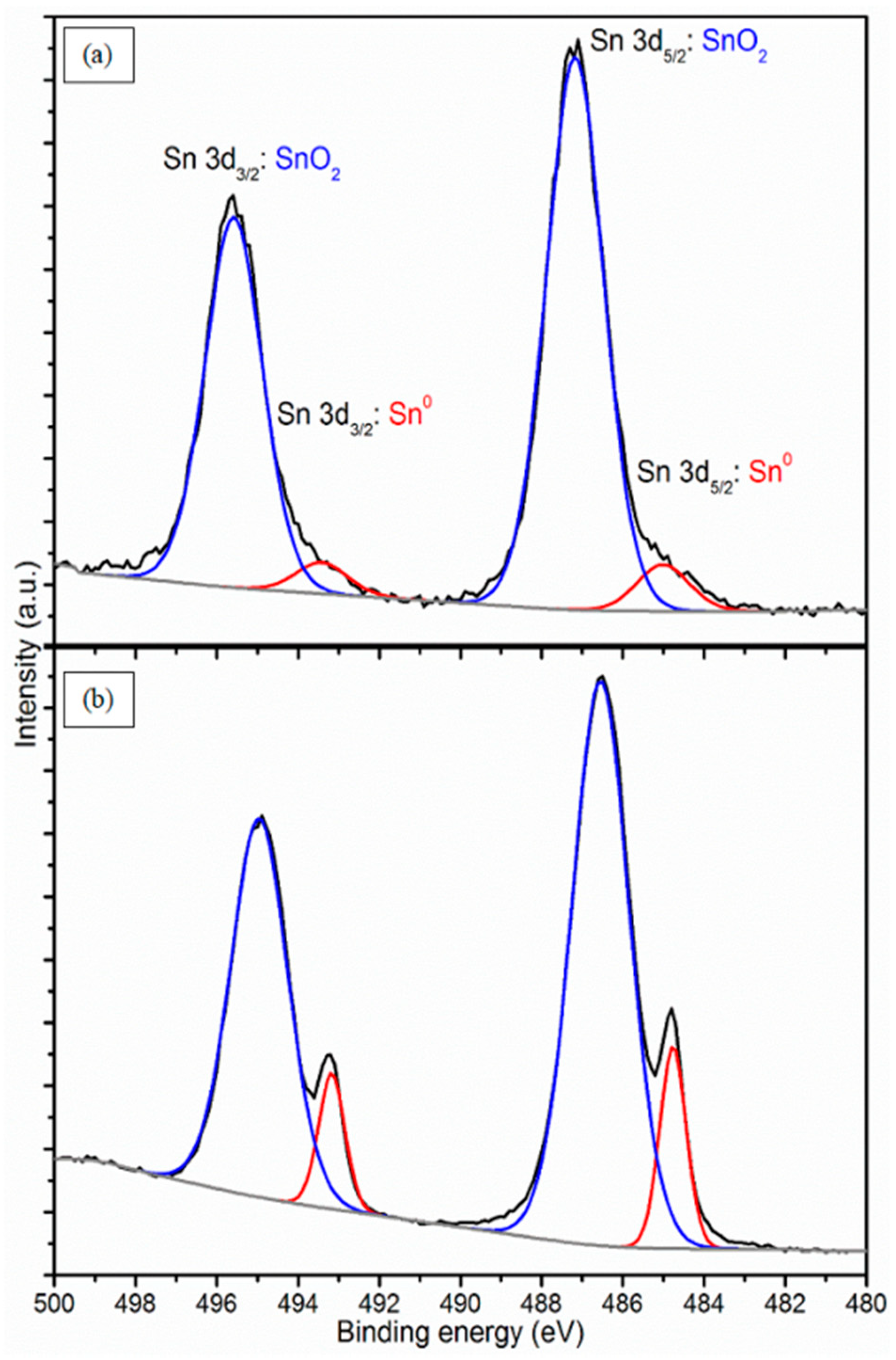
3.4. Atomic Concentration
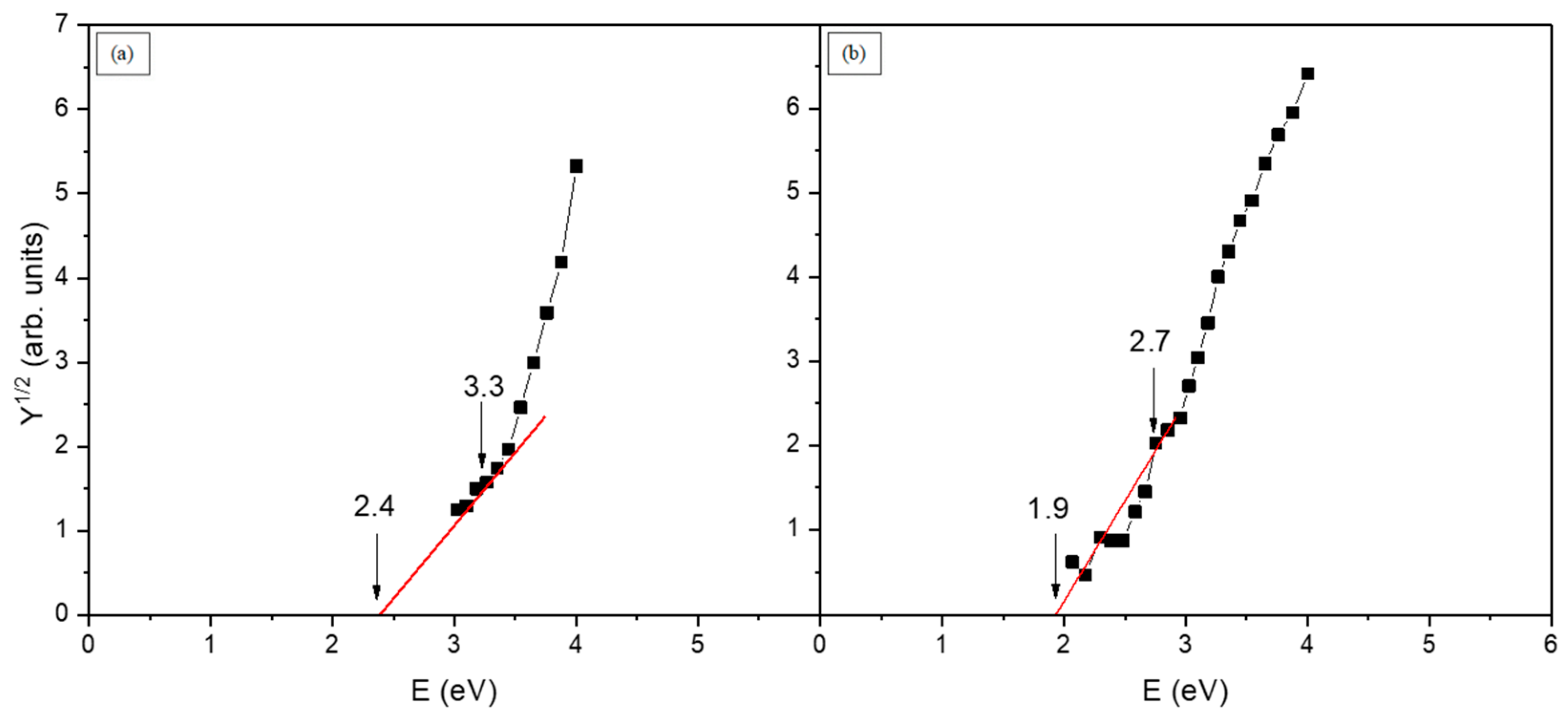
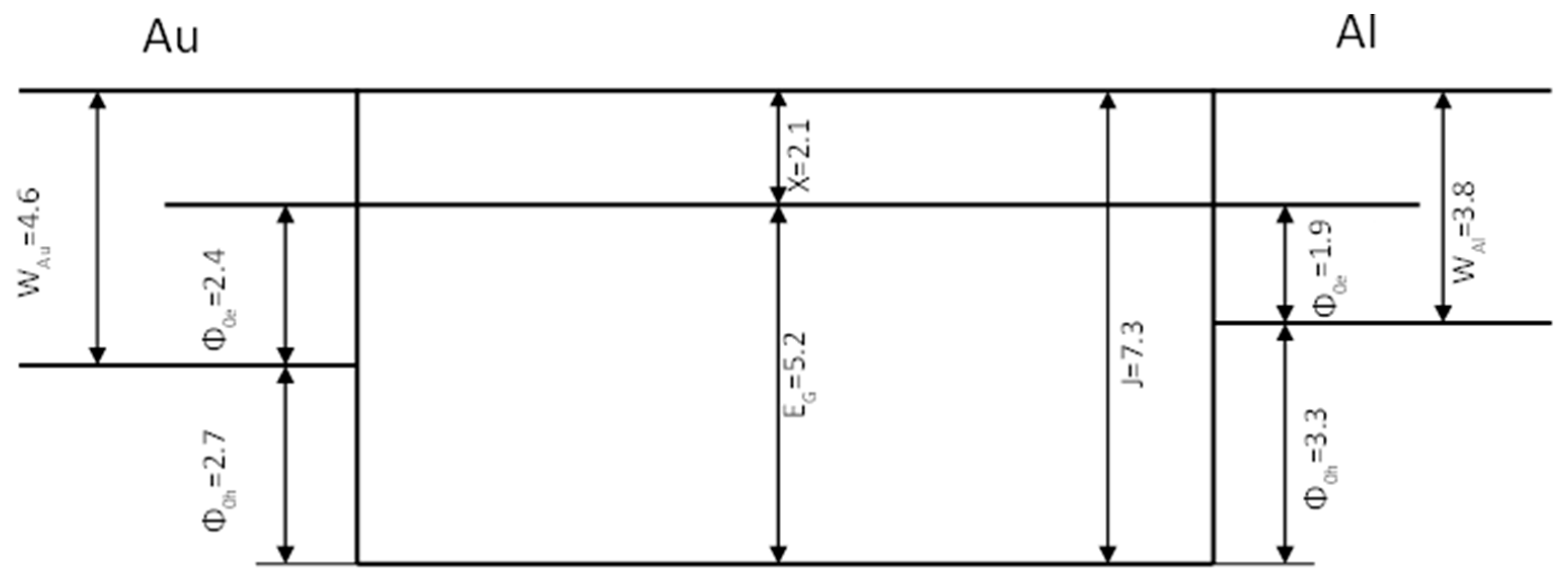
3.5. Internal Photoemission (Photoinjection)
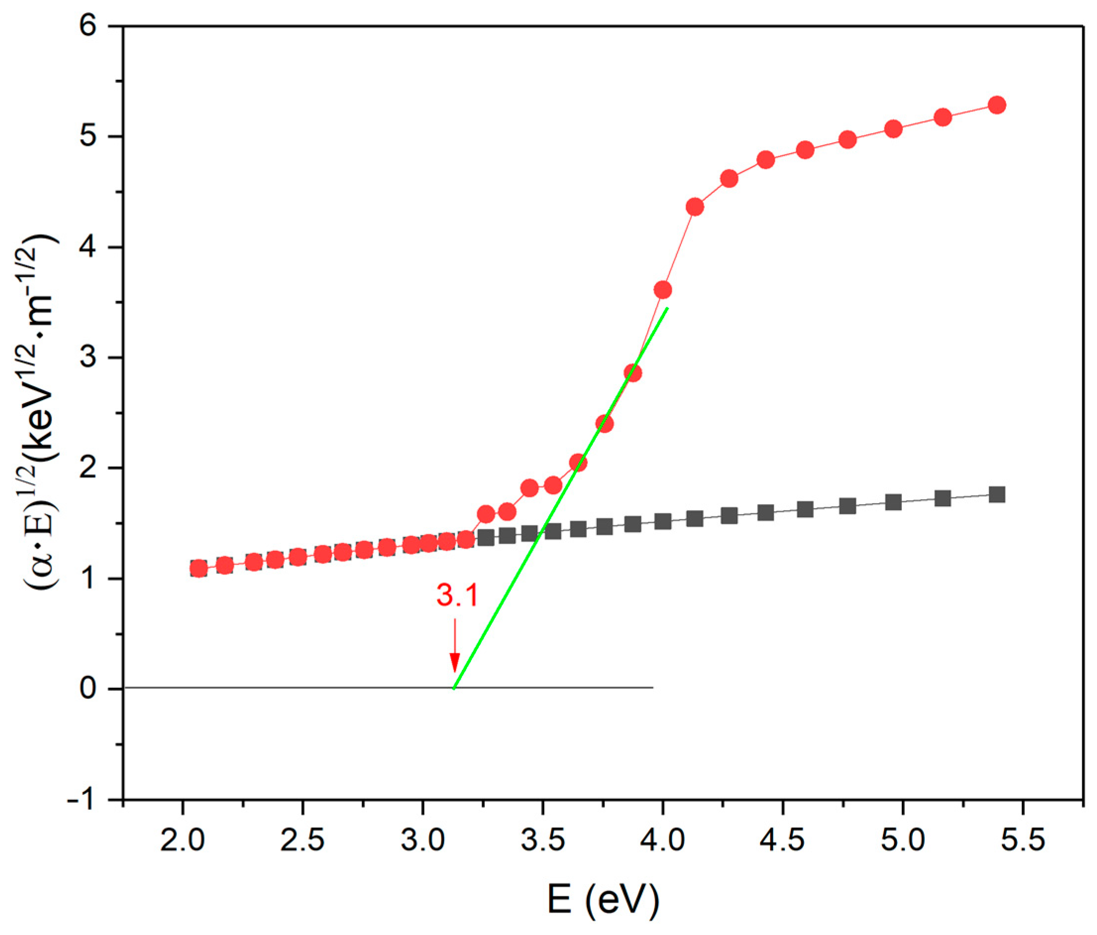
3.6. Optical Absorption
4. Conclusions
Supplementary Materials
Author Contributions
Funding
Institutional Review Board Statement
Informed Consent Statement
Data Availability Statement
Acknowledgments
Conflicts of Interest
References
- Smestad, G.P.; Krebs, F.C.; Lampert, C.M.; Granqvist, C.G.; Chopra, K.L.; Mathew, X.; Takakura, H. Reporting Solar Cell Efficiencies in Solar Energy Materials and Solar Cells. Sol. Energy Mater. Sol. Cells 2008, 92, 371–373. [Google Scholar] [CrossRef]
- Yu, M.; McCulloch, W.D.; Huang, Z.; Trang, B.B.; Lu, J.; Amine, K.; Wu, Y. Solar-Powered Electrochemical Energy Storage: An Alternative to Solar Fuels. J. Mater. Chem. A 2016, 4, 2766–2782. [Google Scholar] [CrossRef]
- Chaikaew, T.; Punyawudho, K. Optimal Voltage of Direct Current Coupling for a Fuel Cell–Battery Hybrid Energy Storage System Based on Solar Energy. Energy Rep. 2021, 7, 204–208. [Google Scholar] [CrossRef]
- Li, Q.; Liu, Y.; Guo, S.; Zhou, H. Solar Energy Storage in the Rechargeable Batteries. Nano Today 2017, 16, 46–60. [Google Scholar] [CrossRef]
- Tang, H.; Chen, C.J.; Huang, Z.; Bright, J.; Meng, G.; Liu, R.S.; Wu, N. Plasmonic Hot Electrons for Sensing, Photodetection, and Solar Energy Applications: A Perspective. J. Chem. Phys. 2020, 152, 220901. [Google Scholar] [CrossRef]
- Gautam, A.; Sk, S.; Pal, U. Recent Advances in Solution Assisted Synthesis of Transition Metal Chalcogenides for Photo-Electrocatalytic Hydrogen Evolution. Phys. Chem. Chem. Phys. 2022, 24, 20638–20673. [Google Scholar] [CrossRef]
- Loget, G.; Mériadec, C.; Dorcet, V.; Fabre, B.; Vacher, A.; Fryars, S.; Ababou-Girard, S. Tailoring the Photoelectrochemistry of Catalytic Metal-Insulator-Semiconductor (MIS) Photoanodes by a Dissolution Method. Nat. Commun. 2019, 10, 3522. [Google Scholar] [CrossRef]
- Suo, S.; Sheehan, C.; Zhao, F.; Xiao, L.; Xu, Z.; Meng, J.; Mallouk, T.E.; Lian, T. Direct Vibrational Stark Shift Probe of Quasi-Fermi Level Alignment in Metal Nanoparticle Catalyst-Based Metal-Insulator-Semiconductor Junction Photoelectrodes. J. Am. Chem. Soc. 2023, 145, 14260–14266. [Google Scholar] [CrossRef]
- Ma, X.C.; Dai, Y.; Yu, L.; Huang, B.B. Energy Transfer in Plasmonic Photocatalytic Composites. Light Sci. Appl. 2016, 5, e16017. [Google Scholar] [CrossRef]
- Wang, H.; Sun, Y.; He, W.; Zhou, Y.; Lee, S.C.; Dong, F. Visible Light Induced Electron Transfer from a Semiconductor to an Insulator Enables Efficient Photocatalytic Activity on Insulator-Based Heterojunctions. Nanoscale 2018, 10, 15513–15520. [Google Scholar] [CrossRef]
- Cui, W.; Chen, L.; Li, J.; Zhou, Y.; Sun, Y.; Jiang, G.; Lee, S.C.; Dong, F. Ba-Vacancy Induces Semiconductor-like Photocatalysis on Insulator BaSO4. Appl. Catal. B 2019, 253, 293–299. [Google Scholar] [CrossRef]
- Tyczkowski, J.; Pietrzyk, B.; Hatanaka, Y.; Nakanishi, Y. Electrical and Optical Properties of Carbon-Tin Films Plasma Deposited from Tetramethyltin in a Three-Electrode Reactor. Appl. Surf. Sci. 1997, 113–114, 534–538. [Google Scholar] [CrossRef]
- Tyczkowski, J.; Kryszewski, M. Photoinjection into Plasma-Polymerised Organosilicon Thin Films: I. Surface States. J. Phys. D Appl. Phys. 1981, 14, 1877–1888. [Google Scholar] [CrossRef]
- Kim, D.W.; Hwang, I.S.; Kwon, S.J.; Kang, H.Y.; Park, K.S.; Choi, Y.J.; Choi, K.J.; Park, J.G. Highly Conductive Coaxial SnO2-In2O3 Heterostructured Nanowires for Li Ion Battery Electrodes. Nano Lett. 2007, 7, 3041–3045. [Google Scholar] [CrossRef] [PubMed]
- Kiruthiga, G.; Rajni, K.S.; Geethanjali, N.; Raguram, T.; Nandhakumar, E.; Senthilkumar, N. SnO2: Investigation of Optical, Structural, and Electrical Properties of Transparent Conductive Oxide Thin Films Prepared by Nebulized Spray Pyrolysis for Photovoltaic Applications. Inorg. Chem. Commun. 2022, 145, 109968. [Google Scholar] [CrossRef]
- Nadolska, A.; Kowalczyk, D.A.; Lutsyk, I.; Piskorski, M.; Krukowski, P.; Dąbrowski, P.; Le Ster, M.; Kozłowski, W.; Dunal, R.; Przybysz, P.; et al. Electrostimulation and Nanomanipulation of Two-Dimensional MoO3-x Layers Grown on Graphite. Crystals 2023, 13, 905. [Google Scholar] [CrossRef]
- Romero, M.; Huerta, L.; Akachi, T.; Llamazares, J.L.S.; Escamilla, R. X-ray Photoelectron Spectroscopy Studies of the Electronic Structure of Superconducting Nb2SnC and Nb2SC. J. Alloys Compd. 2013, 579, 516–520. [Google Scholar] [CrossRef]
- Tyczkowski, J.; Zielinski, M.; Kryszewski, M. On the Mechanism of Electrical Conduction in Glow Discharge Polysilazane Films. Thin Solid Films 1978, 55, 253–259. [Google Scholar] [CrossRef]
- Tyczkowski, J.; Ledzion, R. Electronic Band Structure of Insulating Hydrogenated Carbon-Germanium Films. J. Appl. Phys. 1999, 86, 4412–4418. [Google Scholar] [CrossRef]
- Tyczkowski, J.; Kryszewski, M. Photoinjection into Plasma-Polymerised Thin Organosilicon Films: II. The Structure of Energy Levels. J. Phys. D Appl. Phys. 1984, 17, 2053. [Google Scholar] [CrossRef]
- Bardeen, J. Surface States and Rectification at a Metal-Semiconductor Contact. Phys. Rev. 1947, 71, 717–727. [Google Scholar] [CrossRef]
- Caywood, J.M. Photoemisssion from Metal Contacts into Anthracene Crystals: A Critical Review. Mol. Cryst. Liquid. Cryst. 1970, 12, 1–16. [Google Scholar] [CrossRef]
- Tauc, J.; Grigorovici, R.; Vancu, A. Optical Properties and Electronic Structure of Amorphous Germanium. Phys. Stat. Sol. 1966, 15, 627–637. [Google Scholar] [CrossRef]


| Sample | O [%at] | C [%at] | Sn [%at] | Sn:O |
|---|---|---|---|---|
| Semiconducting SnO2–C | 31.0 ± 0.2 | 43.1 ± 0.6 | 25.9 ± 0.8 | 0.84 ± 0.03 |
| Insulating SnO2–C | 26.6 ± 0.5 | 63.3 ± 0.3 | 10.1 ± 0.3 | 0.38 ± 0.02 |
| Parameters of Insulating Films | Energy (eV) |
|---|---|
| Au contact barrier for electrons Φ0e | 1.9 |
| Au contact barrier for holes Φ0h | 2.7 |
| Al contact barrier for electrons Φ0e | 2.4 |
| Al contact barrier for holes Φ0h | 3.3 |
| Transport gap (Φ0e + Φ0h) | 5.2 |
| Optical gap | 3.1 |
| Electron affinity Χ | 2.1 |
| Ionization potential J | 7.3 |
Disclaimer/Publisher’s Note: The statements, opinions and data contained in all publications are solely those of the individual author(s) and contributor(s) and not of MDPI and/or the editor(s). MDPI and/or the editor(s) disclaim responsibility for any injury to people or property resulting from any ideas, methods, instructions or products referred to in the content. |
© 2024 by the authors. Licensee MDPI, Basel, Switzerland. This article is an open access article distributed under the terms and conditions of the Creative Commons Attribution (CC BY) license (https://creativecommons.org/licenses/by/4.0/).
Share and Cite
Frątczak, E.Z.; Balcerzak, J.; Rogala, M. Optoelectronic Properties of Cold Plasma-Deposited, Oxidized Sn–C Thin Films. Materials 2024, 17, 314. https://doi.org/10.3390/ma17020314
Frątczak EZ, Balcerzak J, Rogala M. Optoelectronic Properties of Cold Plasma-Deposited, Oxidized Sn–C Thin Films. Materials. 2024; 17(2):314. https://doi.org/10.3390/ma17020314
Chicago/Turabian StyleFrątczak, Ewelina Zofia, Jacek Balcerzak, and Maciej Rogala. 2024. "Optoelectronic Properties of Cold Plasma-Deposited, Oxidized Sn–C Thin Films" Materials 17, no. 2: 314. https://doi.org/10.3390/ma17020314
APA StyleFrątczak, E. Z., Balcerzak, J., & Rogala, M. (2024). Optoelectronic Properties of Cold Plasma-Deposited, Oxidized Sn–C Thin Films. Materials, 17(2), 314. https://doi.org/10.3390/ma17020314