

Taguchi Optimization of Wetting, Thermal and Mechanical Properties of Sn-1.0wt.%Ag-0.5wt.%Cu Alloys Modified with Bi and Sb


Abstract
1. Introduction
2. Experiment
2.1. Synthesis, Microstructure, and Thermal Analysis
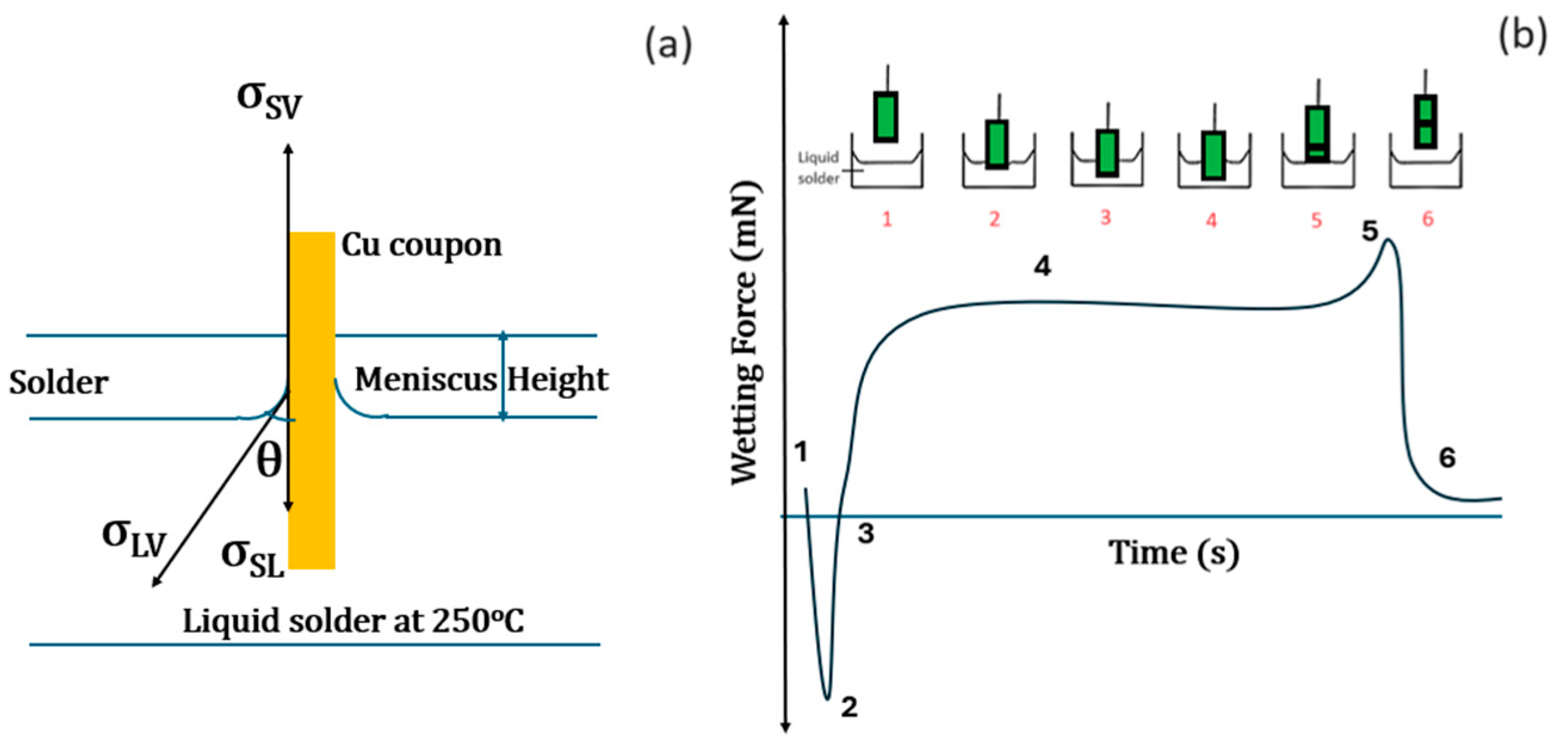
2.2. Wetting Balance Test
2.3. Tensile Strength Test
2.4. Taguchi Optimization
3. Results and Discussion
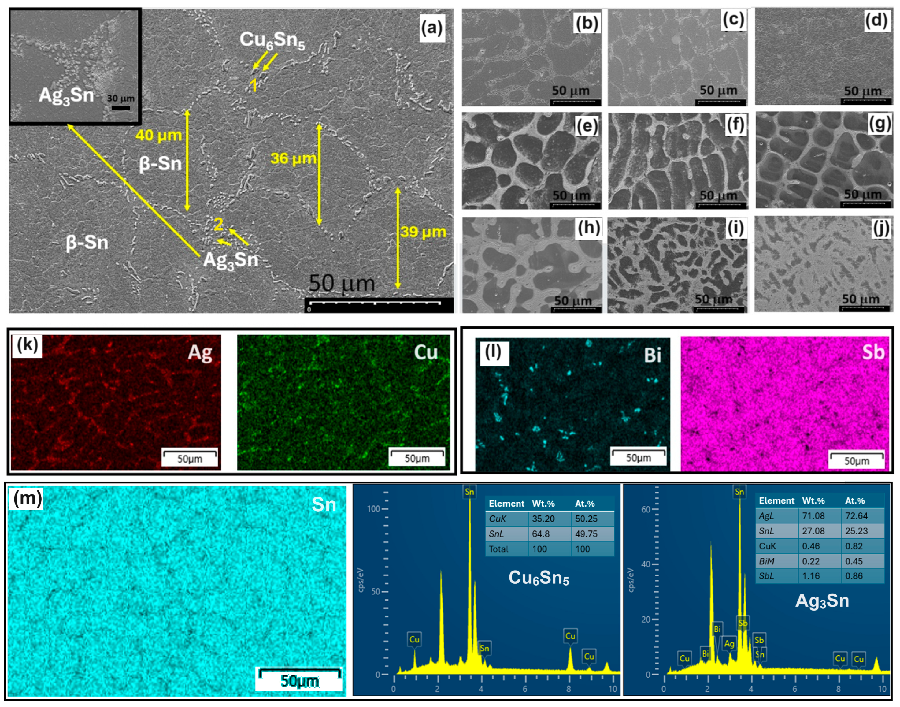
3.1. Microstructure
3.2. Wettability
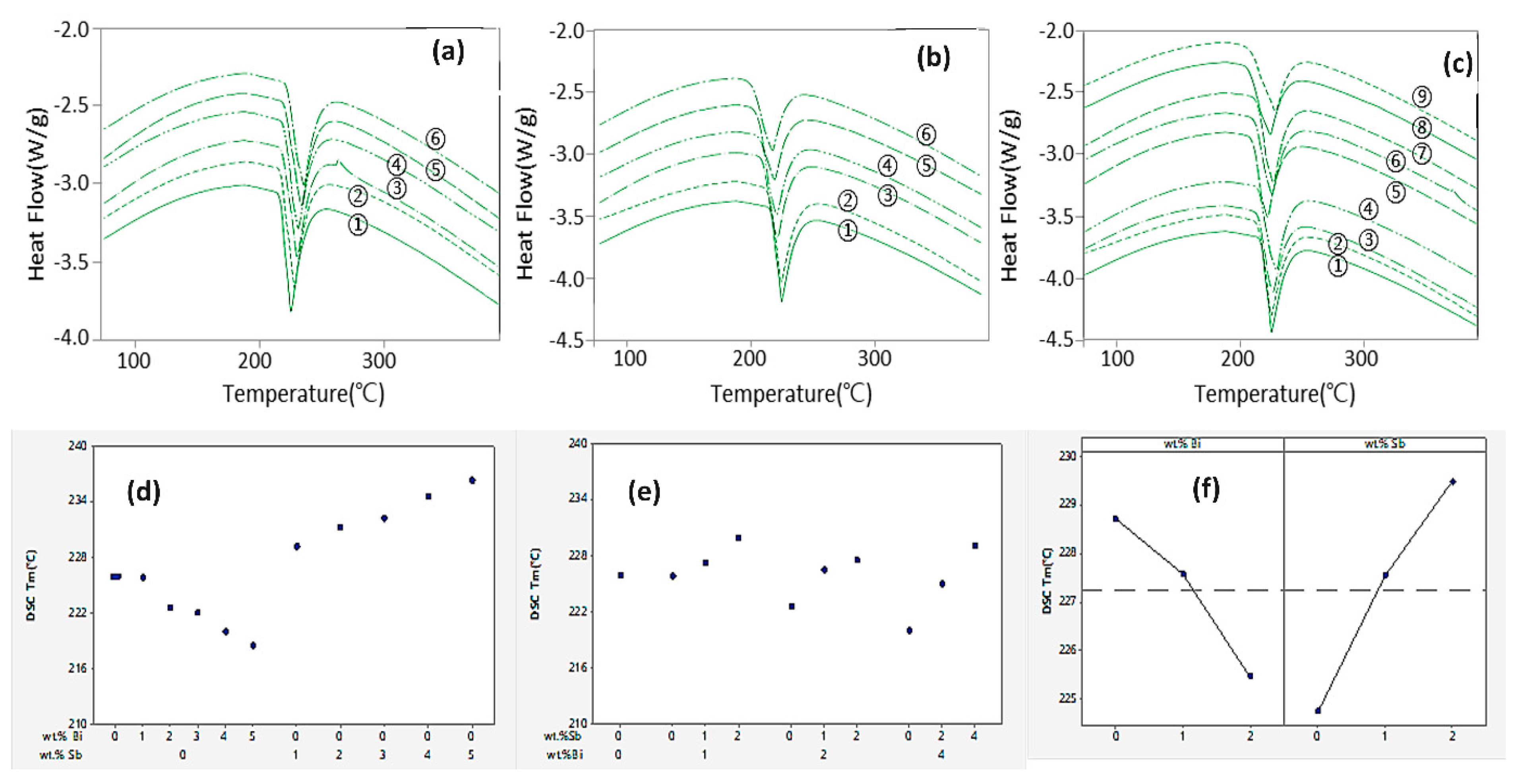
3.3. Melting Point
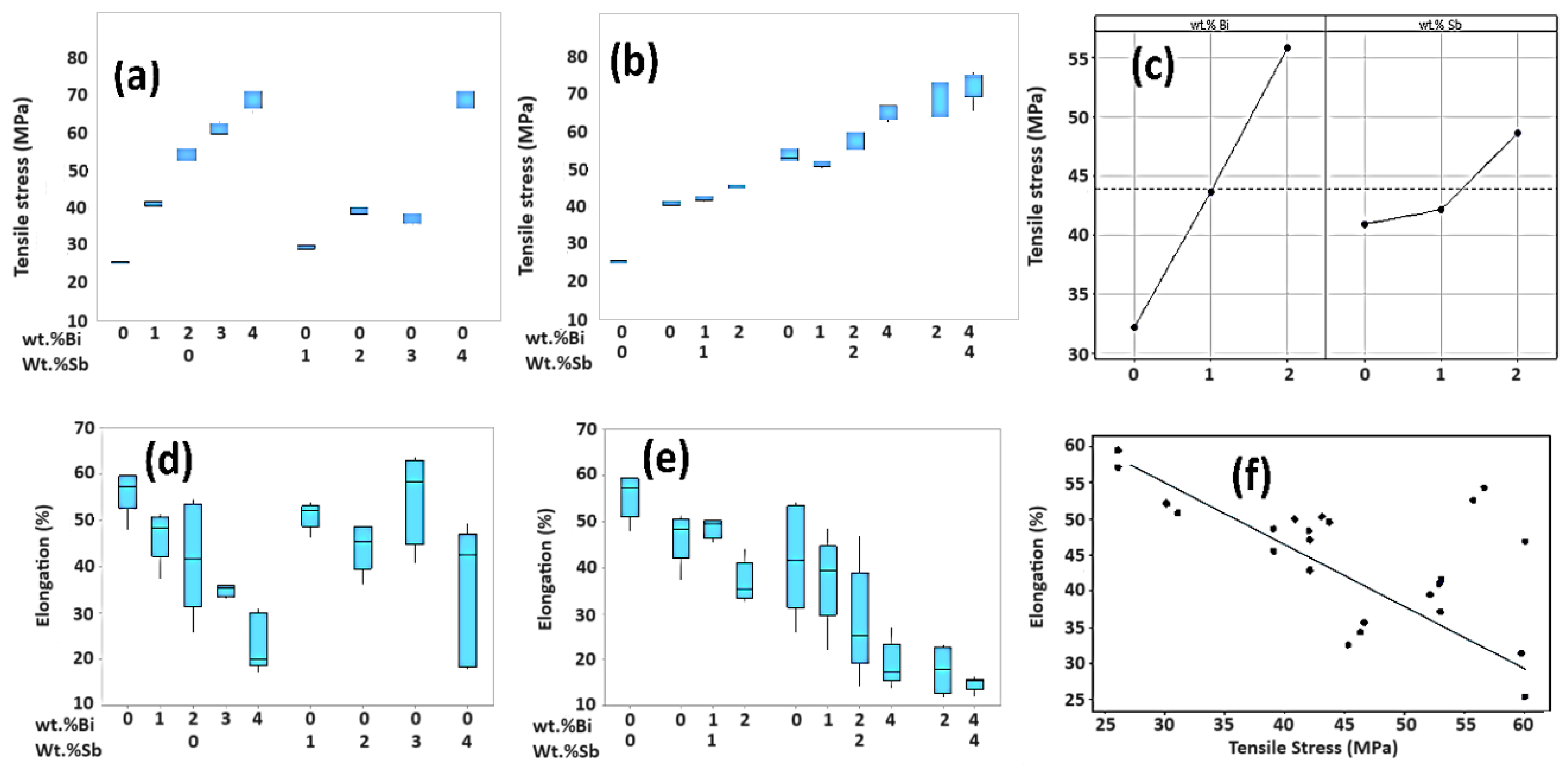
3.4. Tensile Test
4. Conclusions
- The incorporation of Bi and Sb slightly depressed the melting point of the SAC105 alloy. However, when the Bi and Sb are added in combination into SAC105, the melting point showed a drastic reduction which is beneficial to low temperature soldering.
- The wetting balance tests demonstrated that the addition of 2 wt.% of Bi and Sb enhanced the wetting of SAC105 alloys. The combined addition of Bi + Sb showed a more pronounced wetting up to 2 wt.%Sb and Bi.
- The addition of 2 wt.% of Bi and Sb into SAC105 slowed the growth of Sn grains and Ag3Sn IMCs without forming any Bi- or Sb-compounds. The β-Sn grain size and IMCs are refined with the addition of Bi or Sb, Bi being a stronger grain refiner than Sb.
- This study demonstrates that the mechanical properties, UTS and %El, could be significantly controlled when Bi and Sb are embedded into the SAC105 alloy. However, it should be noted that the fraction of Bi and Sb should not exceed 2 wt.% for better realization of properties.
- The Taguchi optimization method predicted a set of combination of properties for better realization of soldering properties to be 2 wt.%Bi and 0 wt.%Sb; ZCT = 0.9 s, wetting point of 222.55 °C, UTS of 55 MPa, and %El of 50%.
Author Contributions
Funding
Institutional Review Board Statement
Informed Consent Statement
Data Availability Statement
Conflicts of Interest
References
- Bharath Krupa Teja, M.; Sharma, A.; Das, S.; Das, K. A review on nanodispersed lead-free solders in electronics: Synthesis, microstructure and intermetallic growth characteristics. J. Mater. Sci. 2022, 57, 8597. [Google Scholar] [CrossRef]
- Zeng, K.; Tu, K.N. Six Cases Reliability Study of Pb-Free Solder Joints in Electronic Packaging Technology. Mater. Sci. Eng. R 2002, 38, 55. [Google Scholar] [CrossRef]
- Abtew, M.; Selvaduray, G. Lead-free solders in microelectronics. Mater. Sci. Eng. R 2000, 27, 95–141. [Google Scholar] [CrossRef]
- Ki, Y.S.; Kim, H.-I.I.; Kim, J.M.; Shin, Y.E. Prediction of thermal fatigue life on mBGA solder joint using Sn–3.5Ag, Sn–3.5Ag–0.7Cu, Sn–3.5Ag–3.0In–0.5Bi solder alloys. JWJ 2003, 21, 92–98. [Google Scholar]
- Park, J.H.; Lee, H.Y.; Jhun, J.H.; Cheon, C.S.; Jung, J.P. Characteristics of Sn–1.7Bi–0.7Cu 0.6In lead-free solder. JWJ 2008, 26, 43–48. [Google Scholar]
- Moon, J.W.; Kim, M.-I.I.; Jung, J.P. A study on the soldering characteristics of Sn–Ag Bi–In ball in BGA. JWJ 2002, 20, 99–103. [Google Scholar]
- Xu, S.; Chan, Y.C.; Zhang, K.; Yung, K.C. Interfacial intermetallic growth and mechanical properties of carbon nanotubes reinforced Sn3.5Ag0.5Cu solder joint under current stressing. J. Alloys Compd. 2014, 595, 92–102. [Google Scholar] [CrossRef]
- Lee, T.Y.; Choi, W.J.; Tu, K.N.; Jang, J.W.; Kuo, S.M.; Lin, J.K.; Frear, D.R.; Zeng, K.; Kivilahti, J.K. Morphology, kinetics, and thermodynamics of solid-state aging of eutectic SnPb and Pb-free solders (Sn–3.5Ag, Sn–3.8Ag–0.7Cu and Sn–0.7Cu) on Cu. J. Mater. Res. 2002, 17, 291–301. [Google Scholar] [CrossRef]
- El-Daly, A.A.; Fawzy, A.; Mansour, S.F.; Younis, M.J. Novel SiC nanoparticles containing Sn-1.0Ag-0.5Cu solder with good drop impact performance. Mater. Sci. Eng. A 2013, 578, 62–71. [Google Scholar] [CrossRef]
- Terashima, S.; Tanaka, M.; Tatsumi, K. Thermal fatigue properties and grain boundary character distribution in Sn-xAg-0.5Cu (x = 1, 1.2 and 3) lead free solder interconnects. Sci. Technol. Weld. Join. 2008, 13, 61–65. [Google Scholar]
- Terashima, S.; Kariya, Y.; Hosoi, T.; Tanaka, M. Effect of silver content on thermal fatigue life of Sn-xAg-0.5Cu flip-chip interconnects. J. Electron. Mater. 2003, 32, 1527–1533. [Google Scholar] [CrossRef]
- Lee, H.Y.; Sharma, A.; Kee, S.H.; Lee, Y.W.; Moon, J.T.; Jung, J.P. Effect of aluminium additions on wettability and intermetallic compound (IMC) growth of lead free Sn (2 wt.% Ag, 5 wt.% Bi) soldered joints. Electron. Mater. Lett. 2014, 10, 997–1004. [Google Scholar] [CrossRef]
- Fouzder, T.; Chan, Y.; Chan, D.K. Influence of cerium oxide (CeO2) nanoparticles on the microstructure and hardness of tin–silver–copper (Sn–Ag–Cu) solders on silver (Ag) surface-finished copper (Cu) substrates. J. Mater. Sci. Mater. Sci. 2014, 25, 5375–5387. [Google Scholar] [CrossRef]
- Xiong, M.; Zhang, L. Interface reaction and intermetallic compound growth behavior of Sn-Ag-Cu lead-free solder joints on different substrates in electronic packaging. J. Mater. Sci. 2019, 54, 1741–1768. [Google Scholar] [CrossRef]
- Tsao, L.C.; Chang, S.Y. Effects of Nano-TiO2 additions on thermal analysis, microstructure and tensile properties of Sn3.5Ag0.25Cu solder. Mater. Des. 2010, 31, 990. [Google Scholar] [CrossRef]
- Bhattacharya, S.; Sharma, A.; Das, S.; Das, K. Synthesis and properties of pulse electrodeposited lead-free tin-based Sn/ZrSiO4 nanocomposite coatings. Metall. Mater. Trans. A 2016, 47, 1292–1312. [Google Scholar] [CrossRef]
- Zhang, L.; Sun, L.; Han, L.; Guo, Y.H. Dorn Creep Model and Finite Element Simulation of SnAgCu-CNT Solder Joints in FCBGA Device. Int. J. Nonlinear Sci. Num. Simul. A 2014, 15, 329–335. [Google Scholar] [CrossRef]
- Sharma, B.; Kumar, M.; Kumar, V.; Sharma, A. Boron nitride nanotubes modified on a lead-free solder alloy for microelectromechanical packaging. ACS Appl. Nano Mater. 2022, 5, 13626–13636. [Google Scholar] [CrossRef]
- Chen, G.; Wu, F.; Liu, C.; Silberschmidt, V.V.; Chan, Y.C. Microstructures and properties of new Sn–Ag–Cu lead-free solder reinforced with Ni-coated graphene nanosheets. J. Alloys Compd. 2016, 656, 500–509. [Google Scholar] [CrossRef]
- Plevachuk, Y.; Poverzhuk, V.; Svec Sr, P.; Svec, P.; Janotová, I.; Janickovic, D.; Rud, A. Electrical Resistivity of Lead-Free Solders Reinforced by Carbon Nanospheres. Int. J. Thermophys. 2024, 45, 31. [Google Scholar] [CrossRef]
- Fine, M. Creep of tin, Sb-solution-strengthened tin, and Sb-Sn precipitate strengthened tin. Metall. Mater. Trans. 2002, 33, 1531–1539. [Google Scholar]
- Li, C.; Yan, Y.; Gao, T.; Xu, G. The microstructure, thermal, and mechanical properties of Sn-3.0Ag-0.5Cu-xSb high-temperature lead-free solder. Materials 2020, 13, 4443. [Google Scholar] [CrossRef] [PubMed]
- Chen, B.L.; Li, G.Y. Influence of Sb on IMC growth in Sn-Ag-Cu-Sb Pb-free solder joints in reflow process. Thin Solid Films 2004, 462, 395–401. [Google Scholar] [CrossRef]
- Kamal, M.; Gouda, E.S.; Marei, L.K. Effect of Bi-content on hardness and micro-creep behavior of Sn-3.5Ag rapidly solidified alloy. J. Exp. Ind. Crystallogr. 2010, 44, 1308–1312. [Google Scholar] [CrossRef]
- Witkin, D.B. Influence of microstructure on quasi-static and dynamic mechanical properties of bismuth-containing lead-free solder alloys. Mater. Sci. Eng. A 2012, 532, 212–220. [Google Scholar] [CrossRef]
- Jaffery, H.A.; Sabri, M.F.M.; Rozali, S.; Mahdavifard, M.H.; Shnawah, D.A. Effect of temperature and alloying elements (Fe and Bi) on the electrical resistivity of Sn-0.7 Cu solder alloy. RSC Adv. 2016, 6, 58010–58019. [Google Scholar] [CrossRef]
- Kisiel, R.; Gasior, W.; Moser, Z.; Pstrus, J.; Bukat, K.; Sitek, J. Electrical and mechanical studies of the Sn-Ag-Cu-Bi and Sn-Ag-Cu-Bi-Sn lead free soldering materials. Arch. Metall. Mater. 2005, 50, 1065–1071. [Google Scholar]
- Delhaise, A. Solid-State Diffusion of Bismuth in Tin-Rich, Lead-Free Solder Alloys. Ph.D. Thesis, University of Toronto, Toronto, ON, Canada, 2018. [Google Scholar]
- Moriuchi, M.; Kariya, Y.; Kondo, M.; Kanda, Y. Class I creep deformation of Sn-Ag-Cu containing solid solution elements and its effect on thermal fatigue life of solder joints. Mater. Trans. 2022, 63, 805–812. [Google Scholar] [CrossRef]
- Shen, L.; Septiwerdani, P.; Chen, Z. Elastic modulus, hardness and creep performance of SnBi alloys using nanoindentation. Mater. Sci. Eng. A 2012, 53, 2811–2822. [Google Scholar] [CrossRef]
- Liu, J.C.; Zhang, G.; Wang, Z.H.; Ma, J.S.; Suganuma, K. Thermal property, wettability and interfacial characterization of novel Sn–Zn–Bi–In alloys as low-temperature lead-free solders. Mater. Des. 2015, 84, 331–339. [Google Scholar] [CrossRef]
- Protsenko, P.; Terlain, A.; Traskine, V.; Eustathopoulos, N. The role of intermetallics in wetting in metallic systems. Scr. Mater. 2001, 45, 1439–1445. [Google Scholar] [CrossRef]
- Zhang, C.; Liu, S.D.; Qian, G.T.; Jian, Z.; Feng, X. Effect of Sb content on properties of Sn—Bi solders. Trans. Nonferrous Met. Soc. China 2014, 24, 184–191. [Google Scholar] [CrossRef]
- Sun, L.; Zhang, L. Properties and Microstructures of Sn-Ag-Cu-X Lead-Free Solder Joints in Electronic Packaging. Adv. Mater. Sci. Eng. 2015, 2015, 639028. [Google Scholar] [CrossRef]
- Shalaby, R.M. Effect of silicon addition on mechanical and electrical properties of Sn-Zn based alloys rapidly quenched from melt. Mater. Sci. Eng. A Struct. Mater. Prop. Microstruct. Process. 2012, 550, 112–117. [Google Scholar] [CrossRef]
- Hasnine, M.; Tolla, B.; Karasawa, M. Effect of Ge addition on wettability, copper dissolution, microstructural and mechanical behavior of SnCu–Ge solder alloy. J. Mater. Sci.-Mater. Electron. 2017, 28, 16106–16119. [Google Scholar] [CrossRef]
- Sayyadi, R.; Naffakh-Moosavy, H. Physical and mechanical properties of synthesized low Ag/lead-free Sn-Ag-Cu-xBi (x = 0, 1, 2.5, 5 wt%) solders. Mater. Sci. Eng. A 2018, 735, 367–377. [Google Scholar] [CrossRef]


| S. No. | Sample | wt.%Bi | S. No. | Sample | wt.%Sb | S. No. | Sample | wt.%Bi, wt.%Sb |
|---|---|---|---|---|---|---|---|---|
| 1 | SAC105 | 0 | 12 | SAC105-1Bi-1Sb | 1, 1 | |||
| 2 | SAC105-1Bi | 1 | 7 | SAC105-1Sb | 1 | 13 | SAC105-1Bi-2Sb | 1, 2 |
| 3 | SAC105-2Bi | 2 | 8 | SAC105-2Sb | 2 | 14 | SAC105-2Bi-1Sb | 2, 1 |
| 4 | SAC105-3Bi | 3 | 9 | SAC105-3Sb | 3 | 15 | SAC105-2Bi-2Sb | 2, 2 |
| 5 | SAC105-4Bi | 4 | 10 | SAC105-4Sb | 4 | 16 | SAC105-2Bi-4Sb | 2, 4 |
| 6 | SAC105-5Bi | 5 | 11 | SAC105-5Sb | 5 | 17 | SAC105-4Bi-2Sb | 4, 2 |
| 18 | SAC105-4Bi-4Sb | 4, 4 | ||||||
| Samples | IMCs Thickness |
|---|---|
| SAC105 | 2.9 ± 0.45 µm |
| SAC105-1Bi | 3.0± 0.51 µm |
| SAC105-2Bi | 3.4 ± 0.57 µm |
| SAC105-4Bi | 3.6 ± 0.69 µm |
| SAC105-1Sb | 2.8 ± 0.35 µm |
| SAC105-2Sb | 2.7 ± 0.29 µm |
| SAC105-4Sb | 2.9 ± 0.32 µm |
| SAC105-2Bi-2Sb | 2.9 ± 0.35 µm |
| SAC105-2Bi-4Sb | 2.6 ± 0.26 µm |
| SAC105-4Bi-2Sb | 2.7 ± 0.27 µm |
| Elements | Sn | Ag | Cu | Bi | Sb |
|---|---|---|---|---|---|
| Atomic radius (nm) | 0.158 | 0.144 | 0.128 | 0.170 | 0.160 |
| Sources | DF | Adj SS | Adj MS | F-Value | p-Value |
|---|---|---|---|---|---|
| Model | 8 | 0.54 | 0.06 | 24.23 | 0.000 |
| Linear | 4 | 0.44 | 0.11 | 39.97 | 0.000 |
| Bi | 2 | 0.08 | 0.04 | 15.04 | 0.000 |
| Sb | 2 | 0.36 | 0.18 | 64.91 | 0.000 |
| Bi + Sb | 4 | 0.09 | 0.02 | 8.49 | 0.000 |
| Model Summary | |||||
| S | R-square | R-S (modify) | R-S (forecast) | ||
| 0.05 | 91.50% | 87.73% | 80.88% | ||
| Sources | DF | Adj SS | Adj MS | F-Value | p-Value |
|---|---|---|---|---|---|
| Model | 4 | 50.342 | 12.5854 | 27.66 | 0.004 |
| Linear | 4 | 50.342 | 12.5854 | 27.66 | 0.004 |
| Bi | 2 | 16.22 | 8.11 | 15.04 | 0.010 |
| Sb | 2 | 34.121 | 17.0607 | 64.91 | 0.003 |
| Bi + Sb | 4 | 1.38 | 2.45 | 12.56 | 0.002 |
| Model Summary | |||||
| S | R-square | R-S (modify) | R-S (forecast) | ||
| 0.67452 | 96.51% | 93.02% | 82.34% | ||
| Tensile Strength | |||||
|---|---|---|---|---|---|
| Sources | DF | Adj SS | Adj MS | F-value | p-value |
| Model | 4 | 2852.71 | 713.18 | 125.64 | 0.000 |
| Linear | 4 | 2852.71 | 713.18 | 125.64 | 0.000 |
| Bi | 2 | 2540.8 | 1270.4 | 223.8 | 0.000 |
| Sb | 2 | 311.91 | 155.96 | 27.47 | 0.000 |
| Bi + Sb | 4 | 124.88 | 5.68 | 30.08 | 0.000 |
| Model Summary—Tensile strength | |||||
| S | R-square | R-S (modify) | R-S (forecast) | ||
| 2.38254 | 95.81% | 95.04% | 93.68% | ||
| Elongation | |||||
| Sources | DF | Adj SS | Adj MS | F-value | p-value |
| Model | 4 | 1492.8 | 373.2 | 15.6 | 0.000 |
| Linear | 4 | 1492.8 | 373.2 | 15.6 | 0.000 |
| Bi | 2 | 575.3 | 287.66 | 12.03 | 0.000 |
| Sb | 2 | 917.5 | 458.73 | 19.18 | 0.000 |
| Bi + Sb | 4 | 526.2 | 23.92 | 9.84 | 0.000 |
| Model Summary—Elongation | |||||
| S | R-square | R-S (modify) | R-S (forecast) | ||
| 1.35492 | 96.24% | 96.09% | 95.74% | ||
Disclaimer/Publisher’s Note: The statements, opinions and data contained in all publications are solely those of the individual author(s) and contributor(s) and not of MDPI and/or the editor(s). MDPI and/or the editor(s) disclaim responsibility for any injury to people or property resulting from any ideas, methods, instructions or products referred to in the content. |
© 2024 by the authors. Licensee MDPI, Basel, Switzerland. This article is an open access article distributed under the terms and conditions of the Creative Commons Attribution (CC BY) license (https://creativecommons.org/licenses/by/4.0/).
Share and Cite
Hong, S.-j.; Sharma, A.; Jung, J.P. Taguchi Optimization of Wetting, Thermal and Mechanical Properties of Sn-1.0wt.%Ag-0.5wt.%Cu Alloys Modified with Bi and Sb. Materials 2024, 17, 2661. https://doi.org/10.3390/ma17112661
Hong S-j, Sharma A, Jung JP. Taguchi Optimization of Wetting, Thermal and Mechanical Properties of Sn-1.0wt.%Ag-0.5wt.%Cu Alloys Modified with Bi and Sb. Materials. 2024; 17(11):2661. https://doi.org/10.3390/ma17112661
Chicago/Turabian StyleHong, Sung-joon, Ashutosh Sharma, and Jae Pil Jung. 2024. "Taguchi Optimization of Wetting, Thermal and Mechanical Properties of Sn-1.0wt.%Ag-0.5wt.%Cu Alloys Modified with Bi and Sb" Materials 17, no. 11: 2661. https://doi.org/10.3390/ma17112661
APA StyleHong, S.-j., Sharma, A., & Jung, J. P. (2024). Taguchi Optimization of Wetting, Thermal and Mechanical Properties of Sn-1.0wt.%Ag-0.5wt.%Cu Alloys Modified with Bi and Sb. Materials, 17(11), 2661. https://doi.org/10.3390/ma17112661