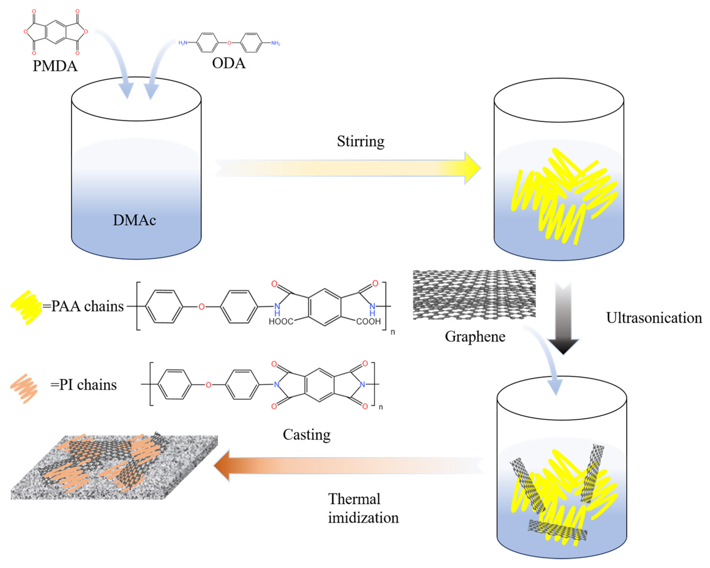
1. Introduction
Since the discovery of graphene, its excellent properties have attracted continuous attention, especially the electrical conductivity of monolayer graphene up to 5 × 10
6 s·m
−1 [
1,
2,
3]. Nowadays, powdered graphene has been widely used in various applications, including electrodes for energy storage devices [
4,
5] and conductive fillers [
6,
7] for polymer nanocomposites. In practice, however, it is often difficult to take advantage of the excellent conductive properties of graphene–polymer composites [
8,
9]. The main reason for this is that the interfacial contact between graphene sheets impedes electrical transmission, so the conductivity of graphene materials is generally much lower than the intrinsic conductivity of a single graphene sheet [
10]. Faced with this problem, some researchers have attempted to introduce similar sp
2-hybridised covalently bonded carbon atom structures to connect graphene sheets while retaining the original excellent in-plane conductivity of graphene. For example, M. M. Slepchenkov and colleagues used single-walled carbon nanotubes to form single-walled carbon nanotube–graphene junctions of different diameters in graphene nanopores, thereby controlling the conductivity of the material [
11]. Another group of researchers built conductive networks using polymer materials as the substrates. For example, J. Y. Suh and his colleagues used the hot pressing method to construct conductive networks with 30 vol% graphene wrapped in polytetrafluoroethylene powder to prepare composites with 7353 s·m
−1 conductivity [
12].
Among the polymers featured in these attempts, polyimide has been used by many researchers as a polymer matrix for graphene composites due to its broad application prospects in the fields of thin-film electrodes [
13,
14,
15], integrated circuit radiators [
16,
17], high-temperature structural materials [
18,
19,
20] and lithium-ion batteries [
21,
22]. Moreover, it has been widely used as one of the best pyrolysis precursors for the preparation of carbon films by carbonisation and graphitisation [
23,
24,
25]. R. K. Biswas et al., have thermally converted polyimide to graphene by writing with a pulsed CO
2 laser on a copper substrate [
26]. However, the composites of graphene and polyimide are not ideally dispersed, often requiring dispersants or modification of the graphene to improve its dispersion and binding in the polyimide matrix [
27,
28]. C. Lim and his colleagues prepared graphene/polyimide films via the electrostatic discharge method and found that the thermal conductivity of the graphene/polyimide films increased exponentially with an increasing graphene content; however, when the graphene content was more than 40 wt%, the graphene/polyimide films could not maintain their shape [
29]. On the other hand, Y. Liu et al., synthesised a 2D monolayer polyimide on a water surface and formed a 2D van der Waals heterostructure through its face-to-face assembly with graphene, which achieved ultrafast interlayer charge transfer through interlayer cation-Π interactions between the 2D polyimide and the graphene [
30]. Z. Xu and his colleagues prepared a series of flexible electrically heated films using polyimide (PI) as a film-forming substrate and graphene as a conductive filler, with the film with 8 wt% graphene rapidly reaching a temperature of 390 °C under a 24 V power supply [
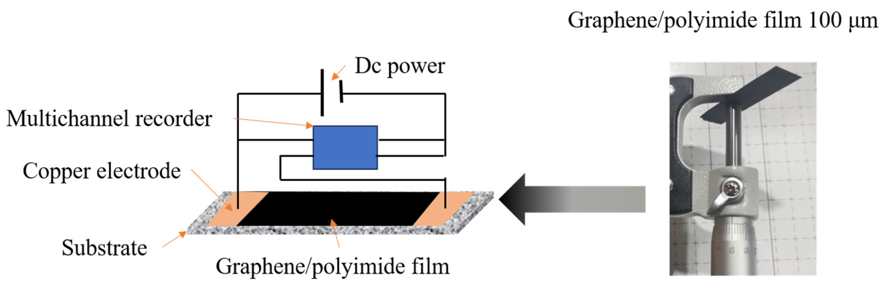
31]. This electrical heating method is called Joule heating [
32,
33]. P. Zhang et al., prepared polyimide/vapour-grown carbon fibre (VGCF) composites via in situ polymerisation and investigated the frequency–temperature relationship between the Joule thermal modulus and the electron transfer mechanism, concluding that thermal fluctuations in the polyimide chain arrangement are small, despite the collision of the electrons with the atoms of the polyimide chains [
34]. Therefore, in the present study, in situ synthesis was used to prepare graphene/polyimide films by the in situ mixing of polyimide precursors with graphene, which ensured the dispersion of the latter. The films were based on a polyimide substrate and a main body of 50 wt% graphene to construct the conductive network. Subsequently, the film was subjected to a simple and fast Joule heating treatment. The polyimide was treated to generate a similar sp
2-hybridised covalently bonded carbon atom structure with graphene as a template, which enhanced the conductive properties of the graphene/polyimide films by ~76.85%.
3. Results and Discussion
The sheet resistance of the raw graphene/polyimide film samples without the Joule heating treatment and the samples of sizes 2.5, 4.0, 5.5 and 7.0 was measured using four-probe resistivity measurements. Each sample was tested three times, and the results are shown below (
Table 1).
The conductivity of the sample can be calculated by the formula [
37,
38]:
where
is the conductivity;
is the resistivity;
is the measured resistance;
is the thickness of the sample;
is the cross-sectional area of the sample; and
is the length of the sample.
The electrical conductivity of the pristine graphene/polyimide film was calculated to be ~1484.79 s·m−1, while the treated graphene/polyimide film had a conductivity of ~2625.84 s·m−1, an enhancement of ~76.85%.
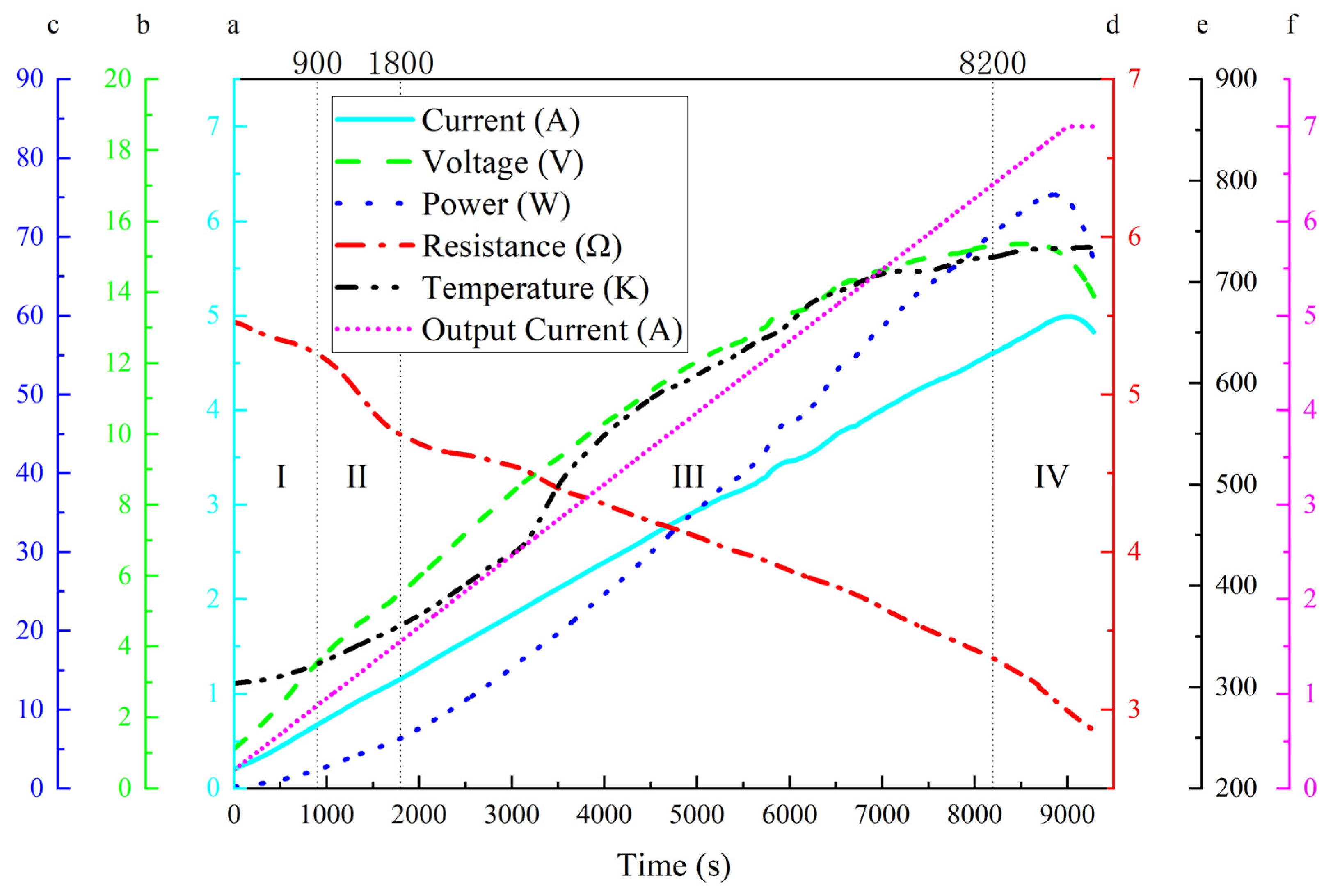
During the Joule heating treatment of the graphene/polyimide films, the input electrical energy was partly converted into thermal energy by the electrothermal effect and partly served as the driving energy for the rearrangement of the atoms in the material. As a result, when the atomic rearrangement was near completion, the power of the material showed a significant decrease as the current continued to increase, as shown in
Figure 3. The current through the sample was less than the output current of the power supply due to the circuit design and the multichannel recorder; this difference increased as the current increased. It is worth noting that while the output current remained at 7.0 A, the current through the sample decreased. This phenomenon may have resulted from the decrease in the shunt of the current through the sample due to the decrease in the resistance. From
Figure 3, it can be observed that the Joule heating process can be divided into four periods: period I, from the start to ~900 s, showing a slow decrease in resistance and relatively fast increases in voltage; period II, from ~900 s to ~1800 s, with an obvious, fast decrease in resistance; period III, from ~1800 s to ~8200 s, with a slow decrease in resistance, a gradually declining rate of voltage increase, and a variational increase in temperature, which inferred a complex collision process between the electrons and the polyimide chains; period IV, from ~8000 s to the end, during which resistance showed an accelerated decrease, voltage, power and current sequentially reached their peaks and then declined, and the increasing temperature trend flattened. This pattern suggests that the change in the internal resistance of the material is produced by multiple factors. An important possible influencing factor is the combined effect of current and heat, causing the excitation of more charge carriers in the graphene/polyimide film as the temperature increases, leading to the phenomenon of a decreasing resistance with increasing temperature. In this study, in the first and third periods, the resistance decline in the graphene/polyimide film was mainly attributed to the temperature increase, which was due to the semiconductor properties of the graphene/polyimide film material, a combination of the quite-high and zero bandgaps of polyimide and graphene, respectively. In the second period, the main influence may have been the atomic rearrangement phenomenon due to the movement of electrons driven by the electric current. The recrystallisation of carbon atoms in the presence of electrons greatly improved electron transport within the material, resulting in a rapid decrease in resistance. The fourth period may have been dominated by the reduction in resistance caused by the large-scale formation of a new graphene/polyimide interface near the end of the atomic rearrangement process. The conductivity measured by the Joule heating method was significantly different from that measured by the four-probe method, mainly due to the resistance change caused by the inevitable temperature increase during Joule thermal experiments. The rest might have been caused by the different contact resistance of the two measurement methods.
During the Joule heating treatment, according to Equation (1), the conductivity of the raw sample was ~7328.69 s·m−1, and that of the sample after Joule heating was ~13,907.28 s·m−1, which was an increase of ~89.76%. This difference, compared to the conductivity registered during the sheet resistivity calculations, may have been due to the current and temperature effects.
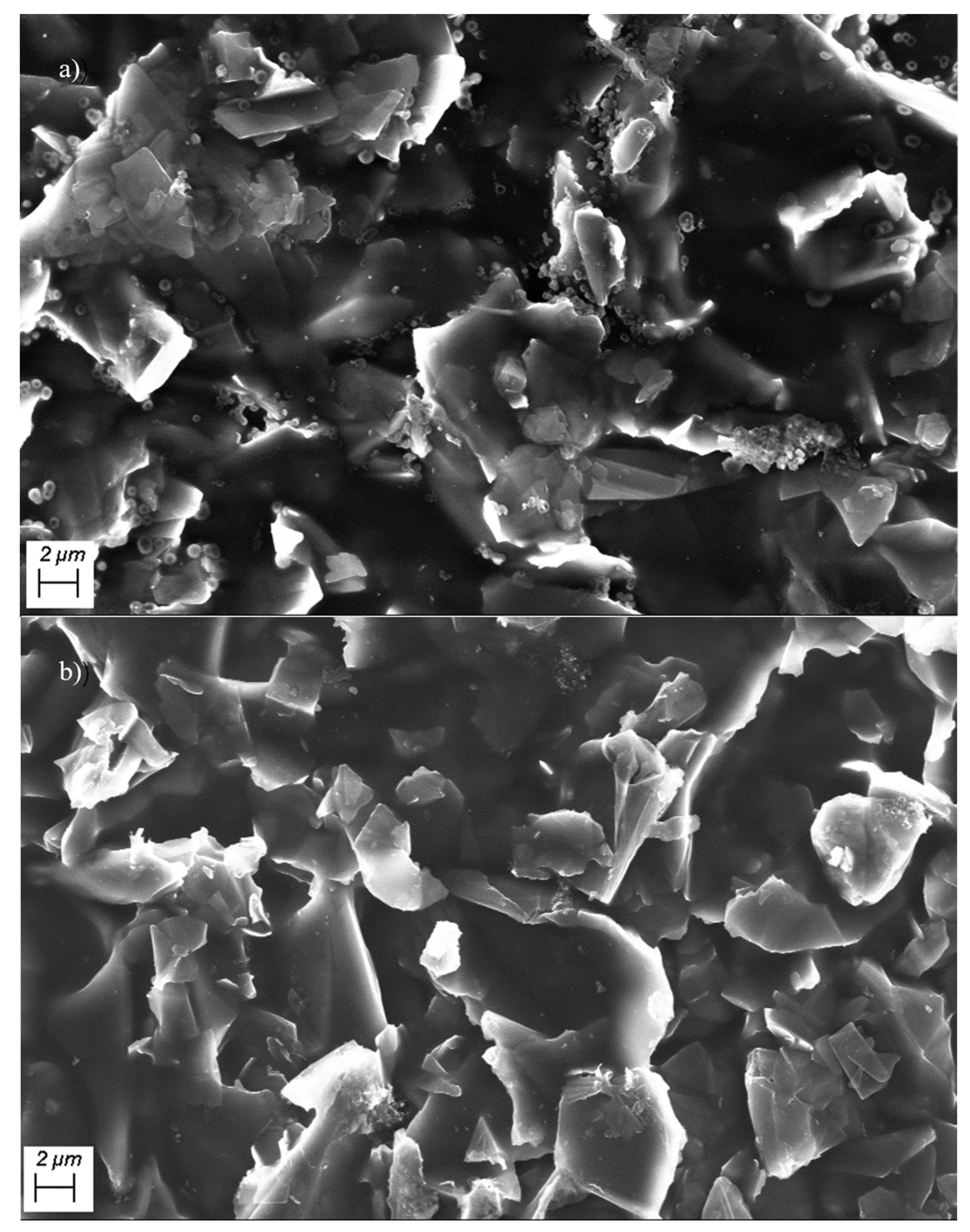
Figure 4a,b show scanning electron microscope (SEM) images of the graphene/polyimide films before and after treatment. As can be seen from the figure, the graphene sheets are stacked together, and, on them, there are irregular gelatinous polyimides. From the structure of graphene/polyimide films at the same scale, the Joule heating treatment did not damage their integrity, as there were no obvious holes and shrinkage. Meanwhile, the more detailed microstructure was observed by transmission electron microscopy.
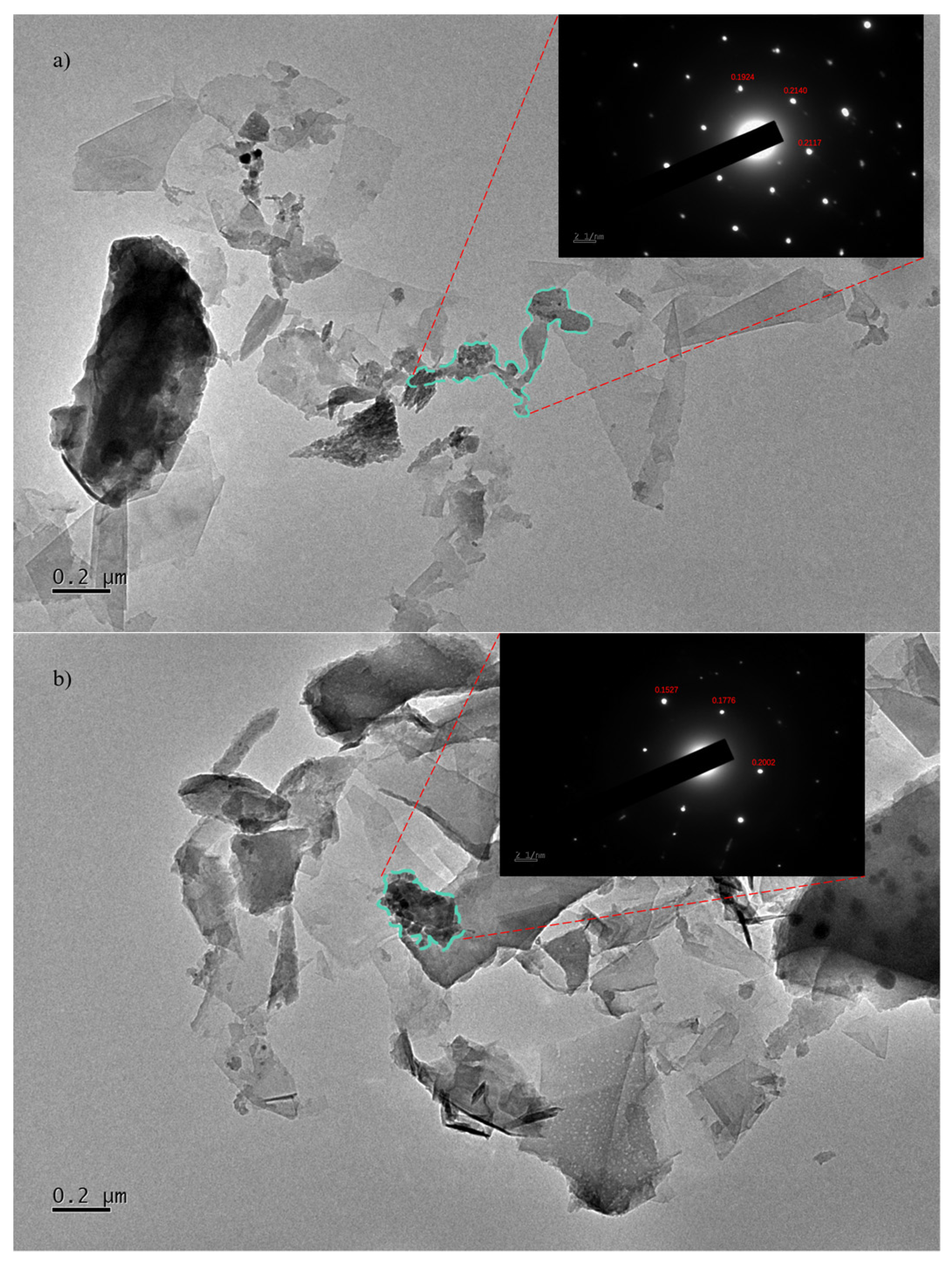
Figure 5a,b include the transmission electron microscope (TEM) images of the graphene/polyimide films before and after treatment. The samples were dispersed with ethanol, treated ultrasonically and, then, placed onto the copper grid. As can be seen in
Figure 5a, the graphene was stacked in a lamellar state, and it maintained a relatively complete and clean edge. Between its lamellae, the graphene was bonded by polyimide. For the selected region electron diffraction (SAED) pattern of the connected parts, a new crystalline diffraction pattern like graphene but with different lattice parameters appeared. This diffraction pattern indicated that the graphene/polyimide thin-film material formed, through the crystallisation of polyimide and using graphene as a template, a new phase resembling a six-membered ring structure during the Joule heating treatment [
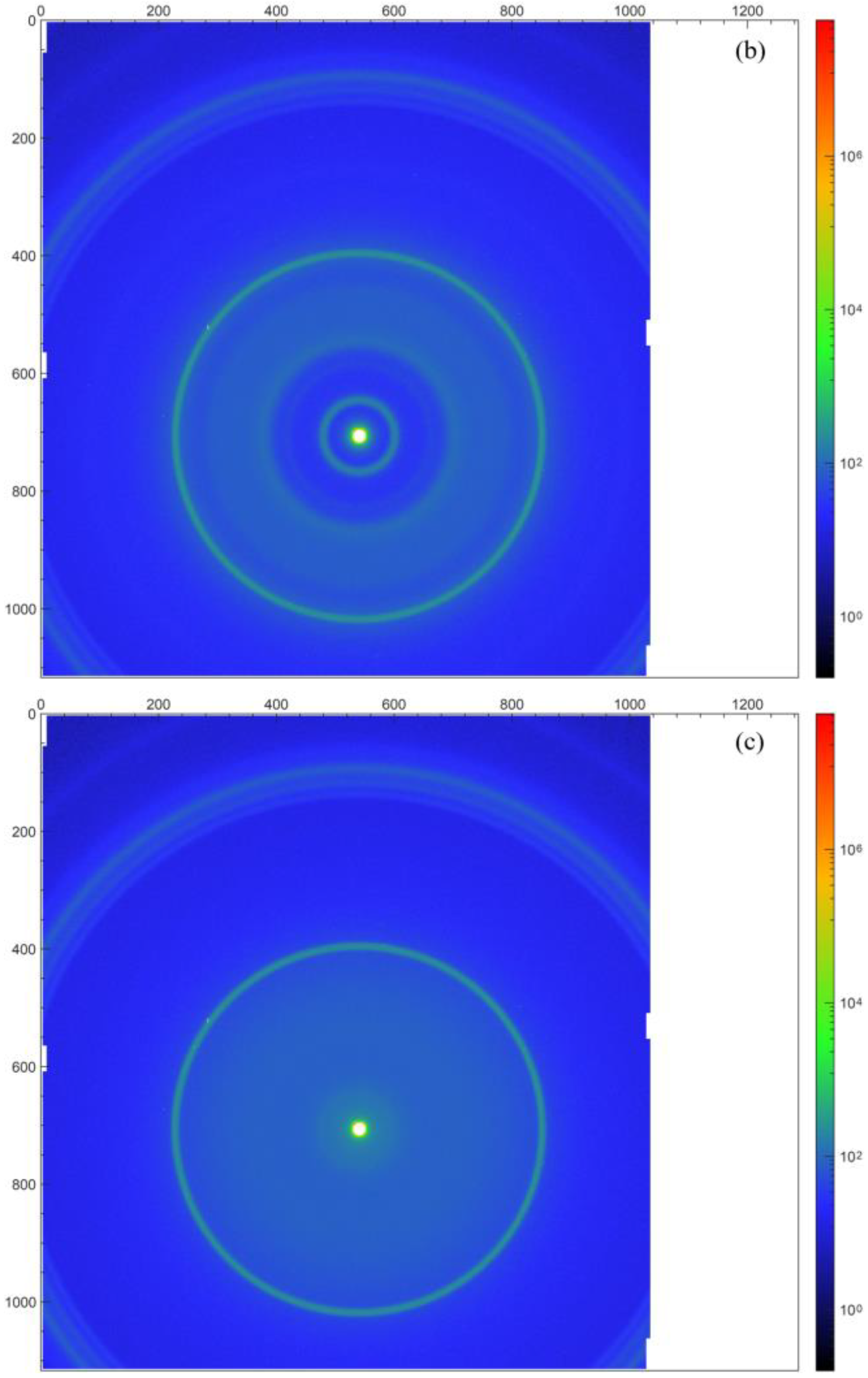
39]. By calibrating the crystal plane’s spacing, it can be seen that the last three spacings of this new phase (0.1527 nm, 0.1776 nm and 0.2002 nm) were smaller than those of the raw sample’s graphene (0.1924 nm, 0.2140 nm and 0.2117 nm).
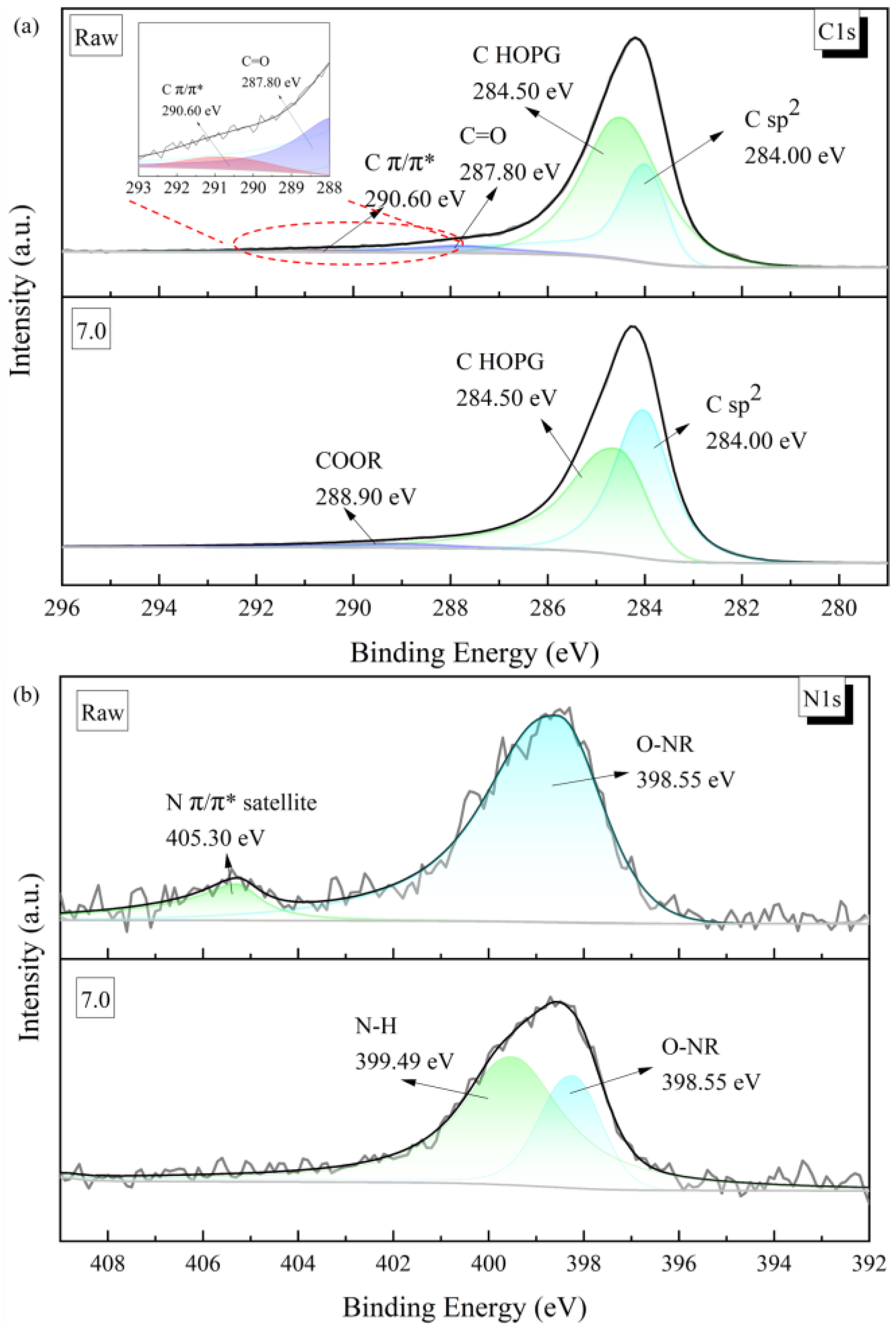
This structural change in the thin-film material was also evident in its electronic structure. As can be seen from the C1s peaks of the materials characterised by X-ray photoelectron spectroscopy (XPS), the graphene/polyimide films both before and after treatment showed clear characteristics of inorganic carbon materials, with the peaks being sharp and asymmetric overall (
Figure 6a). Both of them were characterised by the C sp
2 characteristic peak (284.00 eV), with a highly oriented graphite-like crystal structure. After Joule heating, the C Π/Π* bond (290.60 eV), which was present in the sample in small amounts, disappeared, and a COOR bond (288.90 eV) appeared, which may have been related to the oxidisation of the C=O bond (287.80 eV) in the original material [
40]. Correspondingly, the N1s energy spectra of both materials showed a clear signal from the imide ring (O-NR, 298.55 eV) (
Figure 6b). However, in the original material, there was also a more pronounced peak at 405.30 eV caused by the signal drift in the Π-bond of N in the imide ring. The X-ray photoelectron spectroscopy results indicated some loss and rearrangement of the chemical bonds of C. The recombination of these bonds could have come from the electrons moving, under the influence of an external power source, in the direction of the potential difference, accompanied by the perturbation of the Π-electronic structure inside the material, during the Joule heating treatment. In this process, the electrons would have been driven by the voltage and left the domains throughout the material space, with the consequent re-bonding of the atoms, to form a more stable and oriented crystal structure. From the perspective of the energy bands, as shown in
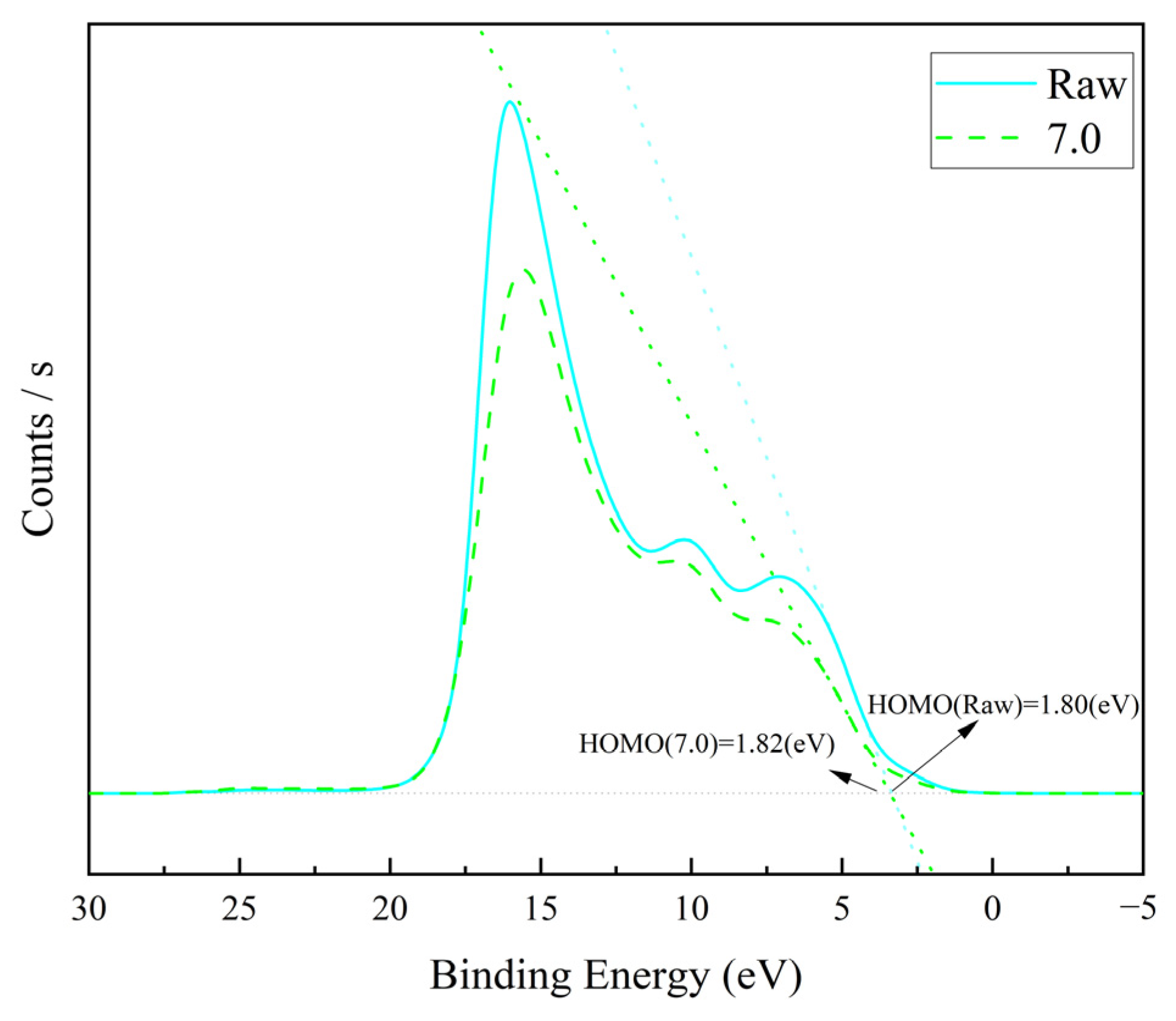
Figure 7, the HOMO orbits of the graphene/polyimide films before and after the Joule heating treatment were close, both about 1.81 eV. Moreover, the band structure of the two was similar, revealing that the Joule heat treatment did not change the band structure of the graphene/polyimide films.
The Raman spectroscopy results of the films showed that the raw samples, the samples during the treatment process, and the already-treated samples exhibited graphene-like spectral features (
Figure 8) [
41]. In particular, three major peaks—D, G and 2D—were found in all the samples, located at ~1350 cm
−1, ~1570 cm
−1 and ~2700 cm
−1, respectively. The D peaks are usually considered to be defect or edge peaks of graphene, involving a process of inelastic intervalley scattering of an iTO phonon near the K point with the intervalley scattering of a defect, which would activate the respiratory vibrational modes of the six-membered ring. The G peak is usually considered to be a characteristic peak of sp
2-hybridised carbon atoms, and it involves the intravalley scattering process of two doubly condensed iTO and iLO phonons near the Γ point. The peak generally arises from an in-plane vibration of the sp
2 carbon atom, corresponding to a vibrational mode with E
2g symmetry. The 2D peak, on the other hand, is produced by two-interval inelastic scattering of troughs from an iTO phonon near the K point, and it is an overtone of the D peak. The 2D band is the second-order D band corresponding to the two phonon lattice vibrations, and it is a characteristic peak of graphene’s structure [
42]. The number of graphene layers can be inferred from the ratio of G/2D band intensities (I
G/I
2D), as well as the shape and position of these bands [
41]. As shown in
Figure 8, the 2D band was not sharp, and the I
G/I
2D value was relatively big, indicating that the graphene sample had a low degree of graphitisation and significant layer-stacking. From the change in the value of I
G/I
2D, the stacking degree of graphene became larger at 4.0 and 5.5 A. This may have been due to the appearance of a new crystalline phase caused by atomic rearrangement during the Joule heating process, which reduced the inelastic cavity scattering of iLO phonons. The new phase took graphene as a template, showing a greater degree of stacking. Then, with the growth of the new crystalline phase, the ratio of I
G/I
2D tended to return to the raw sample’s value. The D’ peak at ~1620 cm
−1 was present in the raw sample. The formation of this peak mainly involved a process of inelastic intravalley scattering of an iLO phonon near the K point, with the intravalley scattering of a defect, suggesting a defect in the raw sample, that disappeared with the Joule heating treatment. It is noteworthy that the G peak first appeared to be red-shifted during the treatment, implying that, in the graphene/polyimide films, during the Joule heating process, the rearrangement of the atomic structure caused by the electrons’ directional movement led to a recrystallisation phenomenon. The increase in crystallinity led to an expansion of the material, resulting in a decrease in the frequency of the phonons interacting with the incident photons. The subsequent blue shift, on the other hand, indicated the formation of a large number of new interfacial layers between the graphene and the recrystallised polyimide, which had a higher phonon frequency. The G peak of the final 7.0 sample showed another small red shift, indicating the gradual stabilisation of the new interface and a slight increase in crystallinity. This phenomenon was also confirmed by the X-ray diffraction (XRD) results (
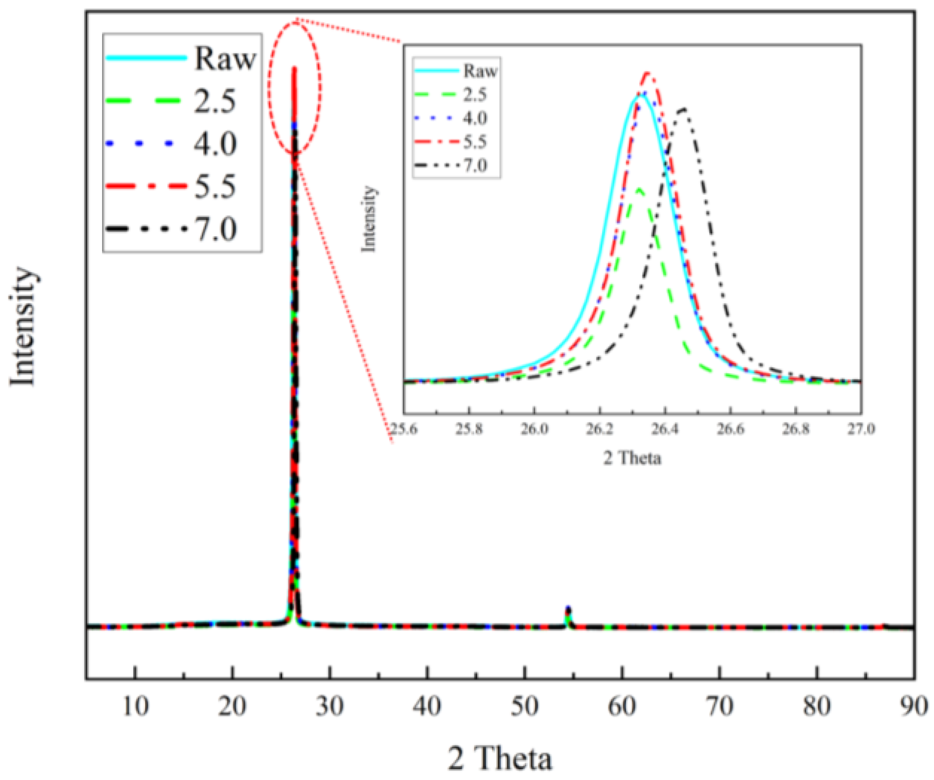
Figure 9), in which it was clear that the main peak of the film was located at the position of the (002) peak and that 2θ was close to 26.4°. It could be seen that, with the Joule heating treatment, the 2θ angle of its Schott peak became larger, indicating smaller lattice spacing and the expansion of the material. Moreover, the treated sample had the largest 2θ angle, which was subject to the double effect of recrystallisation and the formation of a new interfacial layer.
The average grain size (
) in the graphene/polyimide films could be calculated from the intensity ratio of the G and D peaks in the Raman spectrum (
Figure 8) [
43], as follows:
where
is the wavelength of the incident light in the Raman spectrum. From this result, the average grain size in the graphene/polyimide films appeared to increase, then decrease and increase again during the Joule heating treatment, which was supported by the shift in the Raman peak position. Furthermore, the growth of new grains followed the Arrhenius equation [
43], as follows:
where
is the reaction rate of grain growth at a given temperature;
is the prefactor, also known as the Arrhenius constant, in the same units as
;
is the experimental activation energy in J·mol
−1;
is the molar gas constant, =8.314 J·K
−1mol
−1; and
is the reaction temperature.
From the voltage–temperature curve in
Figure 1, it can be seen that the range and variation in the reaction temperature was large, so the correction of Equation (3) was obtained [
44]:
where
is the experimentally measured constant;
is the reaction temperature; and
is the initial reaction temperature. Molecular dynamics calculations show that the temperature at which PI crystals form graphene rings is ~2400 K, and the critical temperature for PI carbonation is around 700 °C [
26]. Therefore, the present graphene/polyimide film did not form graphene rings nor undergo large-scale carbonation, and the whole should have still retained the structure of polyimide, with only some minor atomic rearrangements to form new grains and crystal phases. In this process, graphene improved the aggregation structure of polyimide molecules, forming a crystal structure which was more conducive to electron transport.
The detailed microstructure formed by this localised atomic rearrangement was difficult to capture directly, but it was possible to characterise some of the microstructural differences in the graphene/polyimide thin films before and after Joule heating by wide-angle X-ray scattering (WAXS). The 1D WAXS pattern in
Figure 10a shows the diffraction rings at 1.77 Å
−1 and 2.96 Å
−1 for the graphene/polyimide films both before and after Joule heating. They correspond to d-space values of 3.55 Å and 2.12 Å, respectively, with the former being due to the spacing of the few graphene stacks in the sample and the latter being close to the lattice constant of graphene. The untreated pristine graphene/polyimide film also had three diffraction loops of 0.36 Å
−1, 0.72 Å
−1 and 0.97 Å
−1, corresponding to d-space values of 17.45 Å, 8.73 Å and 6.48 Å, respectively. The two sites at 17.45 Å and 8.73 Å were derived from the same lamellar-stacking spacing structure between the main chains of the polyimide polymer chain caused by the separation of the side-chains. Moreover, the site at 6.48 Å was likely to have been derived from the imide ring. This result suggested that, during the Joule heating treatment, the side-chain structures of some polyimide polymer chains and the imide ring were destroyed and their atomic structures rearranged, resulting in the disappearance of the diffraction rings at these locations. In addition, the diffraction rings of the pristine graphene/polyimide films at 1.77 Å
−1 had a half-peak width slightly larger than that of the graphene/polyimide films after the Joule heating treatment. This indicated that the crystallinity of the graphene in the samples increased after Joule heating.
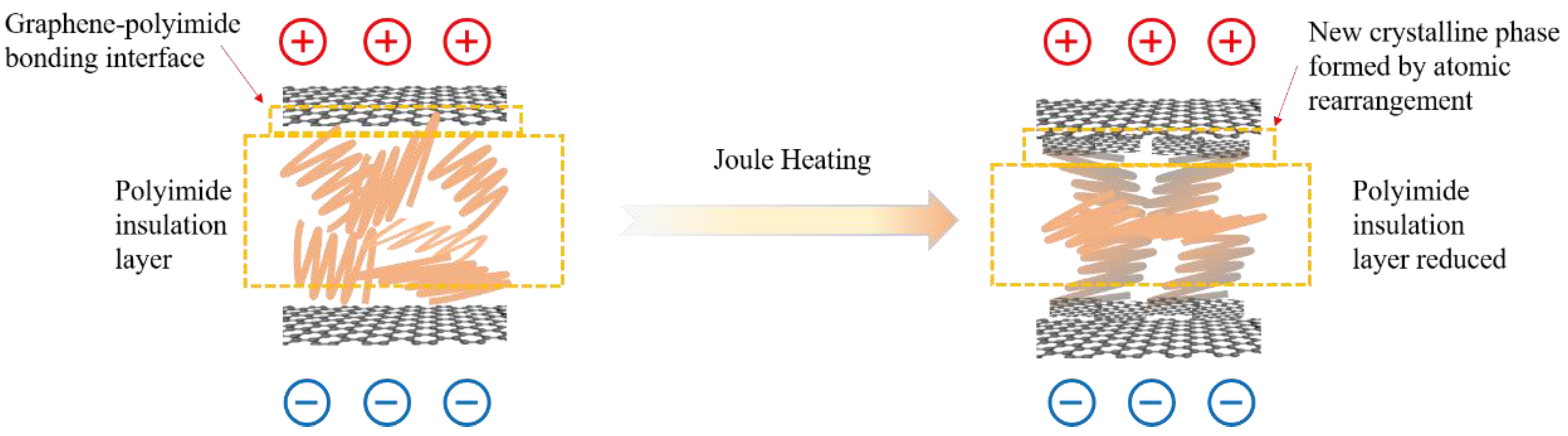
From the above results, it can be inferred that, in the graphene/polyimide film, the graphene lamellae are connected by polyimide, forming a microstructure similar to a double-layer capacitor with graphene as the electrode plate and polyimide as the insulator. As shown in
Figure 11, when a current is applied, the graphene is polarised at both ends. At this point, when the graphene is polarised to a certain extent, a pathway for electron transport is formed, due to the tiny size of the polyimide, coupled with a small number of out-of-domain electrons from the benzene ring on it. When the graphene/polyimide film is subjected to a Joule heating treatment, the crystallinity of the graphene increases. The polyimide does not undergo significant pyrolysis as there are no obvious shrinkage and holes in the films after Joule heating, as shown in
Figure 4, coupled with the fact that no noticeable gas release can be observed during the treatment. The structural changes in the graphene/polyimide films during a Joule heating treatment may be mainly due to the breaking of ether bonds, benzene rings and imide rings [
45] which, once broken, are oriented, to some extent, along the direction of the current. Finally, under the influence of the current, a certain number of rearrangements of the atoms exposed to the current occurs, using the graphene at the interface as a template. On the one hand, this reduces the distance between the graphene in the capacitive structure of the bilayer, thus reducing the resistance. On the other hand, the rearranged atoms that use graphene as a template will provide more off-domain electrons, thus increasing the number of charge carriers. With this synergistic effect, the electron mobility of the graphene/polyimide film is greatly increased after treatment with Joule heating.
The above conclusion can be illustrated using electrochemical impedance spectroscopy (EIS). As shown in
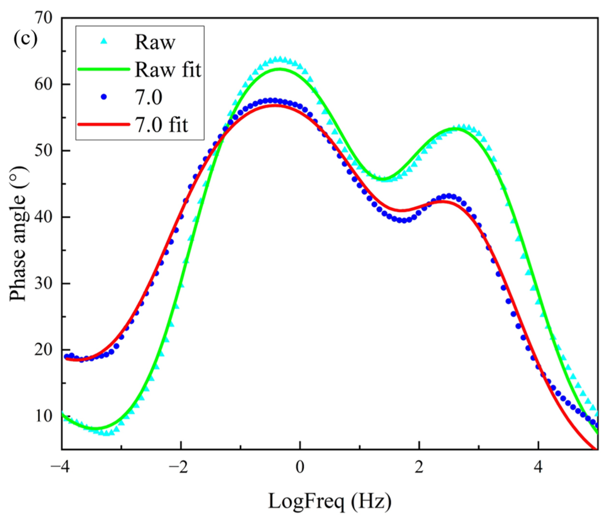
Figure 12, a complex Faraday impedance appears when an AC signal passes through the graphene/polyimide film. In the low-frequency part, the diffusion effect exceeds the electrochemical effect, and a Warburg impedance appears. Meanwhile, in the high-frequency part, part of it manifests as a capacitive arc of the bilayer capacitance, and the other part is the relaxation of the surface state in response to the potential due to the complexity of the graphene/polyimide film interface. The Faraday current appears as a second time constant due to this surface state factor. Moreover, this time constant exhibits capacitive impedance. The electrochemical impedance characteristics of graphene/polyimide films before and after a Joule heating treatment are more consistent. As can be seen in
Figure 12a, both of the semicircles of the raw film were larger than those of the film treated with Joule heating in the Nyquist plot, probably due to the electron transfer impedance and the capacitive impedance of the interfacial time relaxation of the raw film both being larger than those of the treated film. Moreover, because of the larger capacitive reactance, the slope of the straight line representing the Warburg impedance of the raw film in the Nyquist plot was greater. In the Bode plots’ modulus value plots in
Figure 12b, the modulus values of the raw films were always larger than those of the treated films. Moreover, in the low-frequency region, at frequencies <10
−2, the modulus value of the raw film remained almost constant, while the modulus value of the treated film increased with decreasing frequencies, probably due to the greater diffusion of the treated film. In the Bode plot’s phase-angle plot in
Figure 12c, two peaks appeared for both the raw and treated films, indicating the presence of two time constants for both. The first time constant in the high-frequency region >10
2 may have resulted from the impedance of electron transfer within the sample. The second time constant in the mid-frequency range <10
0 may have arisen from the capacitive impedance of the graphene–polyimide interface.
Their equivalent circuits are shown in
Figure 12a, and the original parameters of each equivalent circuit are shown in
Table 2. It can be seen that the internal resistances of the samples before and after treatment were quite close to one another (R1: 9.847 and 10.00, respectively). Their constant phase-angle components, CPE-P, on the other hand, were all around 0.7 (CPE1-P: 0.71187 and 0.66545, CPE2-P: 0.77232 and 0.69409, respectively), indicating that diffusion effects were present in the samples and that Warburg impedance appeared. While CPE-T represents the electrochemically active area of a capacitor, both CPE-T model parameters of the treated samples were almost three times those of the original samples (CPE1-T: 0.00006259 and 0.00019798, CPE2-T: 0.00010222 and 0.00032375, respectively). With respect to the electron transfer impedance in the sample’s Faraday impedance, the R2 (309.10 and 88.32, respectively) and R3 (64,175 and 23,741, respectively) of both of the treated samples’ capacitive impedances were only 1/3 of those of the original samples, indicating that the distance of the electrons travelling through the polyimide was much shorter. In the Warburg impedance, the W-P of the two samples was closer (W-P: 0.26776 and 0.20536, respectively), indicating the existence of Warburg impedance in both samples. W-R (W-R: 383.6 and 30,882.0, respectively) is the coefficient of Warburg impedance in an equivalent circuit. W-T is the diffusion flux of a sample, which is given by the formula L
2/d, where L is the thickness of the diffusion layer, and d is the diffusion coefficient [
46]. The W-T of the treated sample was more than 2500 times that of the original sample (W-T: 1.507 and 3849.000, respectively). This indicated that the thickness of the diffusion layer containing the electrons involved in the reaction was significantly greater than that of the original sample’s layer when the electrons overcame the electron transfer impedance to reach the surface of the sample and diffused by reacting with the ions in the electrolyte in samples treated with Joule heating. In the electrochemical equivalent circuit, R1 was the systematic internal resistance of the electrochemical test system. The first Faraday impedance may have been the capacitive impedance in the graphene/polyimide two-electrode capacitance model. The decrease in R2 may have been due to the reduction in the thickness of the polyimide layer in the model. The second Faraday impedance may have originated from the graphene–polyimide junction interface. The decrease in R3 suggested a decrease in the interface impedance. Moreover, the large increase in W-T suggested an increase in the thickness of the interface capable of electron transfer. Meanwhile, the increase in the electrochemically active area represented by CPE-T predicted an active interfacial reaction. These conclusions are consistent with the above-described reaction model inference.
The effect of a Joule heat treatment on the structure of graphene/polyimide films is irreversible. Moreover, multiple Joule heat treatments can further improve the conductivity of graphene/polyimide films, but the overall effect shows a slowing trend.
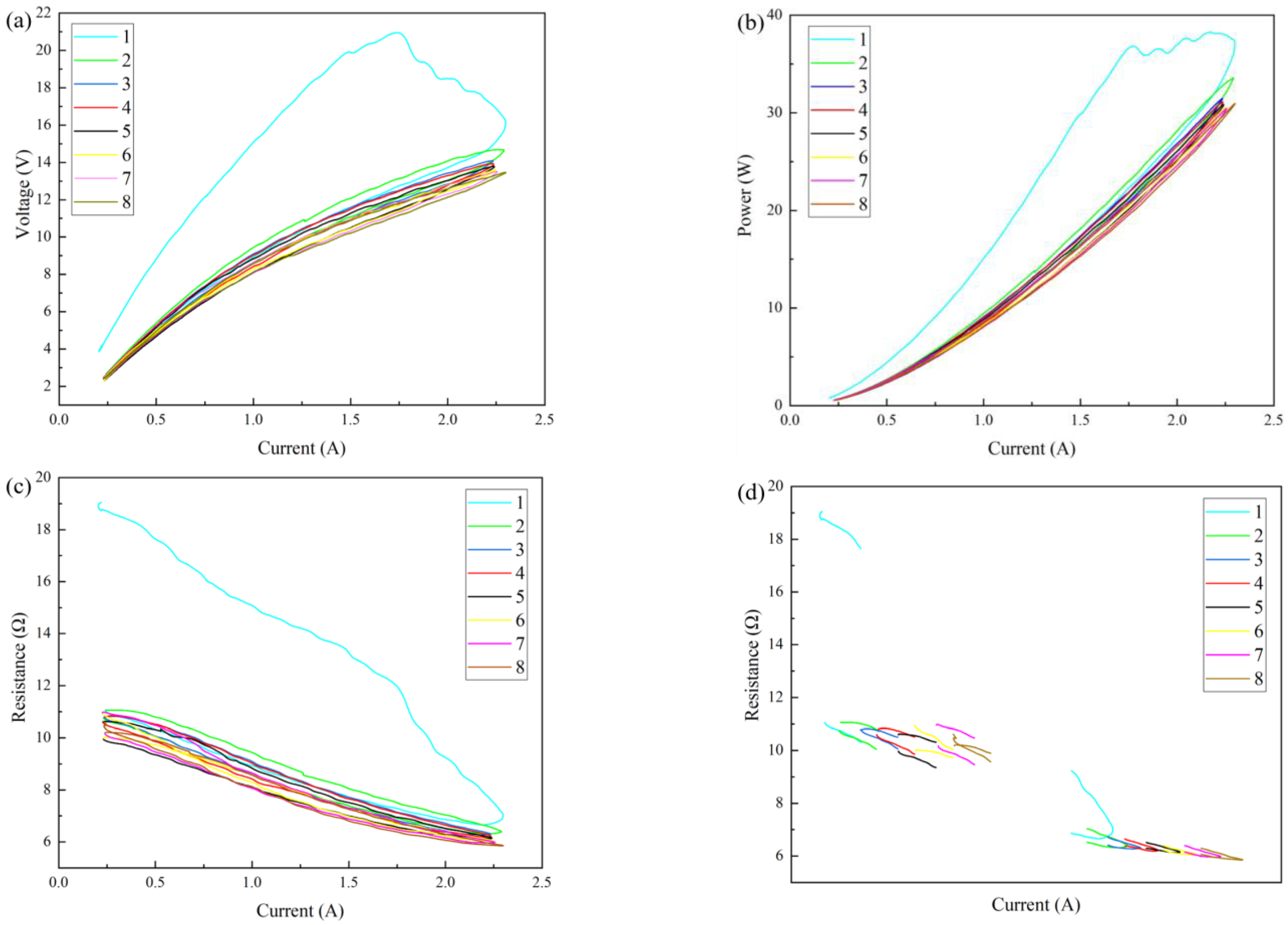
Figure 13a shows the CV curves of the graphene/polyimide films treated with eight Joule thermal cycles. As can be seen from the figure, in the first cycle’s current increase stage, the voltage dropped significantly with the increase in the current. However, according to the CP curve (
Figure 13b), the voltage drop was not synchronised with the power drop. This verified that, under the action of Joule heating, the voltage provided by the external power supply helped the atoms in the graphene/polyimide film to break away from their original positions and rearrange across the energy barrier, which was macroscopic, as the maximum voltage. After that, the electrical energy continued to drive the atoms to complete the rearrangement, so the power continued to increase, while the voltage decreased. This process was not instantaneous and did not occur synchronously throughout the material, so it appeared as a fluctuation in voltage and a wave-like rise in power. According to the current–resistance curve (
Figure 13c), during the first cycle’s current increase stage, the resistance showed an obvious four-stage decline. However, in the first, second and eighth cycles’ current reduction stages, the resistance showed a slow negative correlation with the current change. Specifically, it can be seen from the current–resistance endpoint curve (
Figure 13d) that the resistance was not stable at the beginning and at the end of cycles 2–8. However, when the current of the second to eighth cycles was at a maximum, the resistance was relatively stable, showing a phenomenon of successive reduction, and the reduction trend slowed down. This may have been because, under the synergistic effect of electric heating, a carrier is more excited with an increase in the number of cycles when the current is at a maximum. At the beginning and at the end of a cycle, electron–hole coordination may occur due to the reduced driving force of the excited carrier. However, this process is relatively random, so the resistance at the beginning and at the end of a cycle is unstable. In general, Joule heating changes the atomic structure at the interface of the graphene/polyimide films, causing it to rearrange and form a crystal structure which is more conducive to electron transport. This process is most obvious during the first Joule heat treatment. Moreover, with the increase in Joule heat treatments, the improvement in the films’ conductivity tends to slow down. After the eighth cycle, the conductivity is ~2879.97 s·m
−1, an increase of ~93.94%. It can be inferred that, after a certain number of Joule heating treatments, the interface structure of graphene/polyimide films will be fixed and no longer change with the input current, at which point the conductivity of the graphene/polyimide film would reach its maximum. The sheet resistivity of graphene/polyimide film with eight Joule heating treatment cycles is shown in
Table 3.


