
The Influence of the ITO Layers’ Thicknesses on Their Chosen Physical Surface Parameters


Abstract
:1. Introduction
2. Materials for Investigation
3. Methodology
4. Results and Discussion
5. Conclusions
6. Summary
- From the measurements using the Kelvin probe, the work function Φ of In2O3 does not depend on the layer thickness, while the work function Φ of ITO seems to depend on the thickness of the layer.
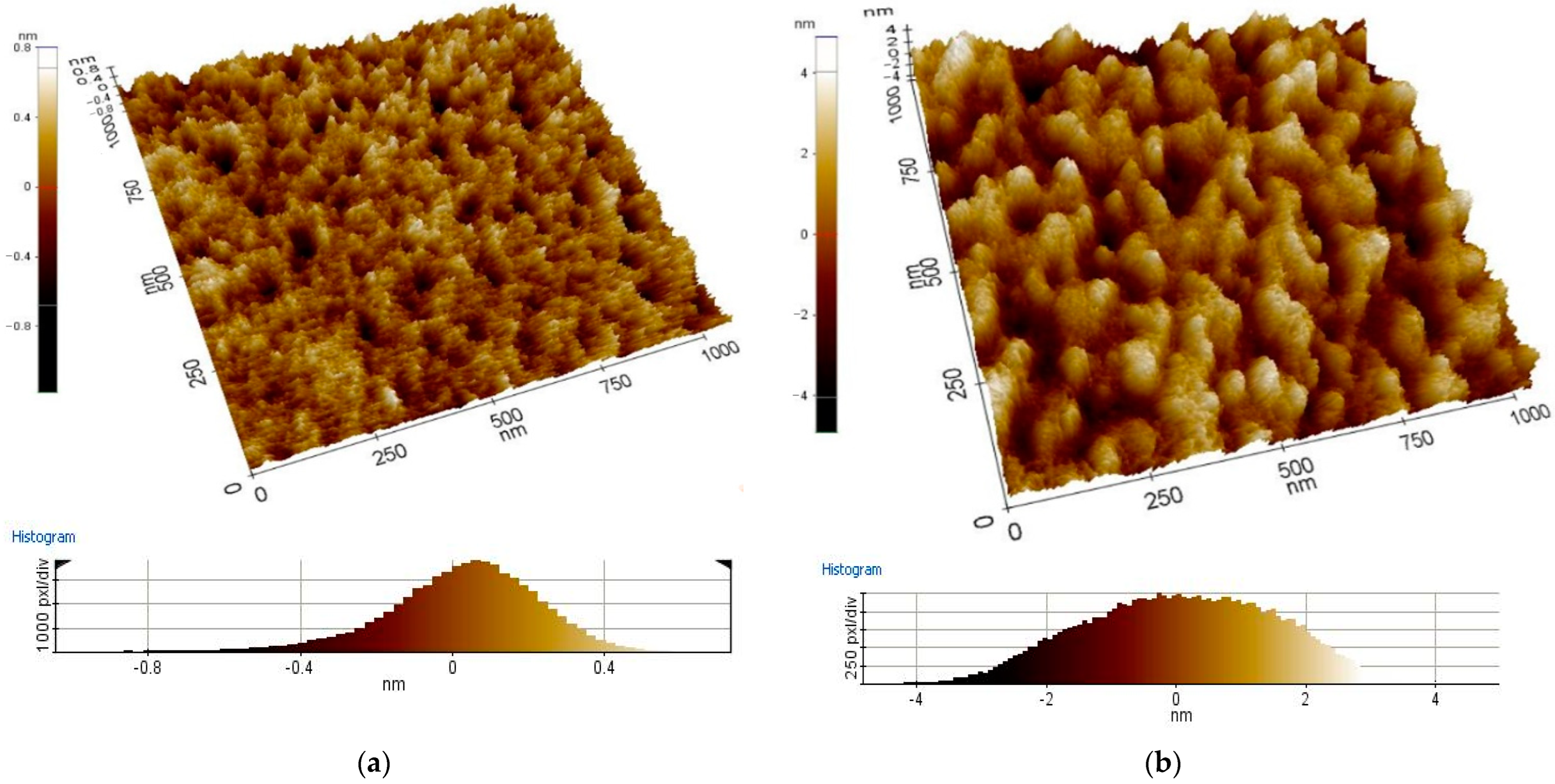
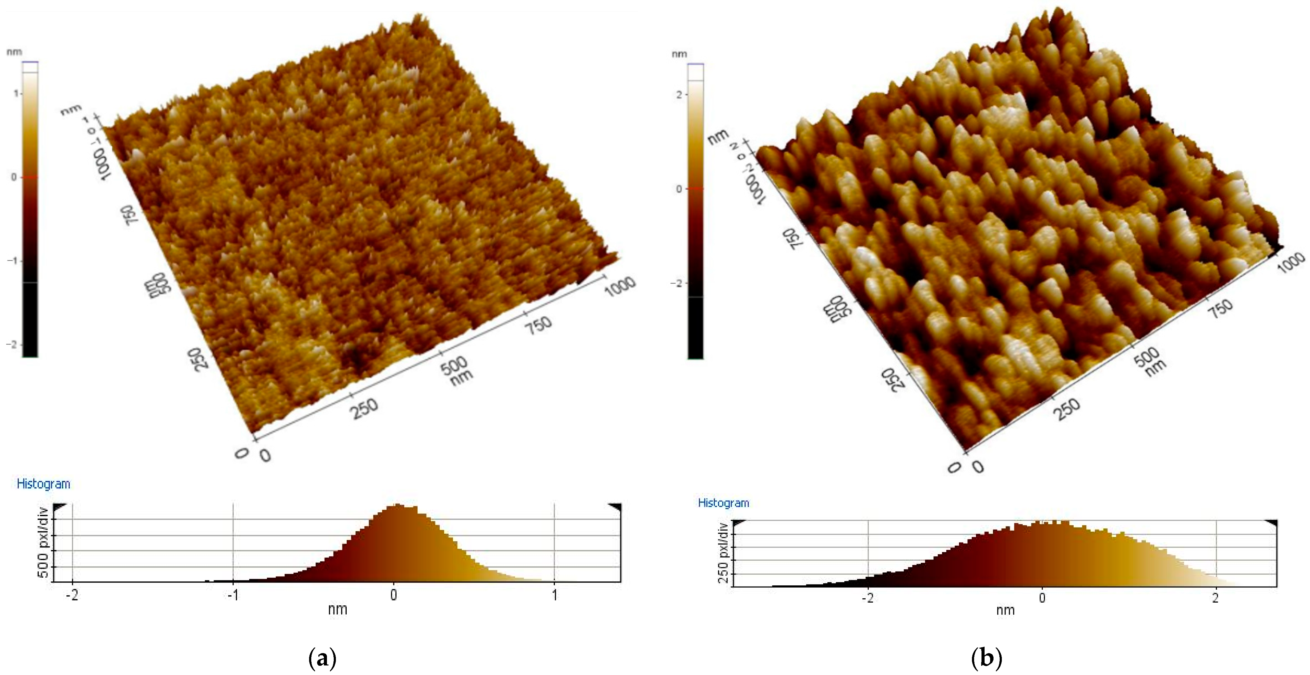
- The results of coating morphology investigations with the use of AFM show the dependence of the coating structure on thickness. It was found that thinner coatings have a structure with a smaller grain size than thicker coatings. It proves that the grains of the tested coating material grow along with the increasing thickness of the coating. Similar phenomena were explained in other works by the Ostwald-Lussac law, for example, in the work [31].
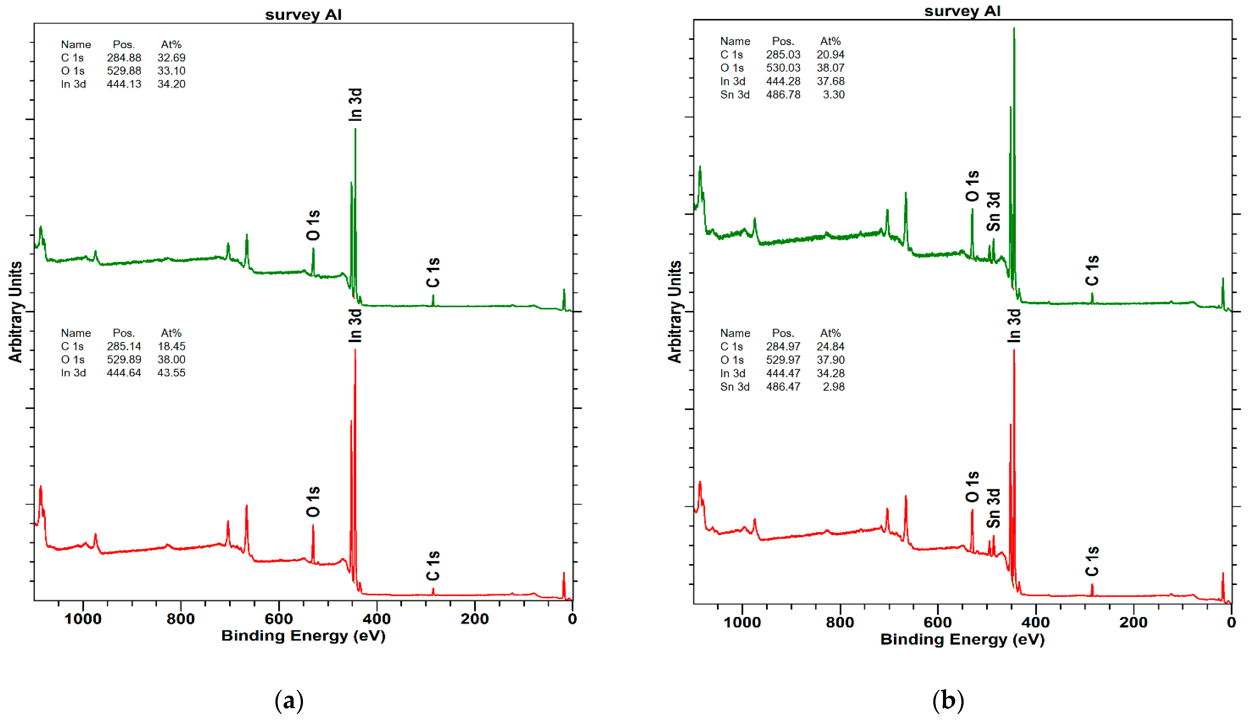
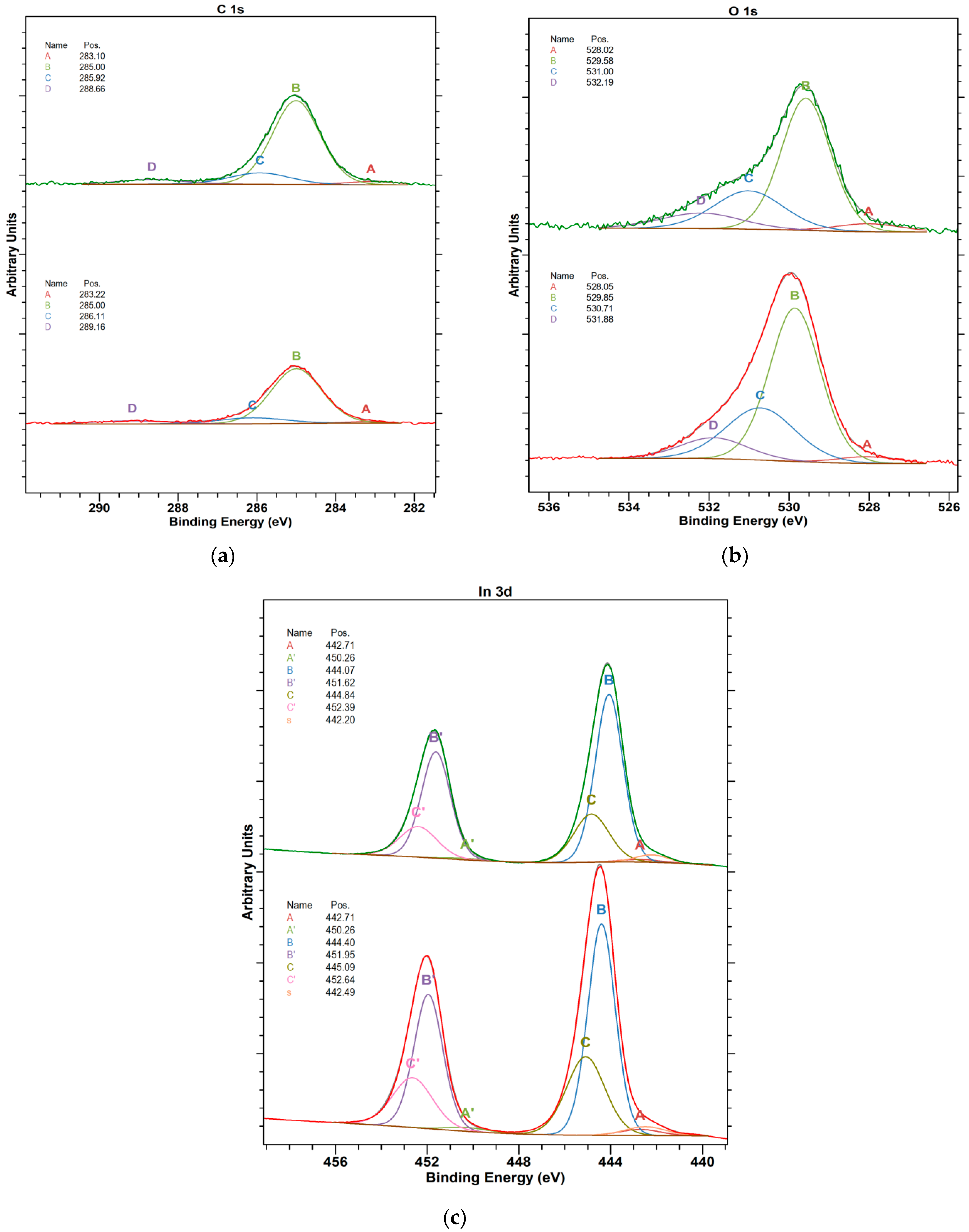
- The Kelvin probe equipped with a light source allows for testing the surface conditions of samples. For example, in photovoltaic materials, surface states play an important role in charge transfer. The depth of analysis of the investigated material is about 2 nm for the Kelvin probe and about 10 nm for XPS. The XPS method shows high sensitivity surface, which comes down to a small analytical depth, which, in the case of metals, is about 5 nm.
- Obtaining a photovoltaic cell with the highest efficiency value is possible by the mutual correlation of the material and technological parameters. The work function, valence band maximum, and electronic states in the band gap are other parameters that need to be investigated in In2O3 and ITO layers, which is also the future aim of the author’s works. We are going to discuss changes in the electronic structure induced by the defects to evaluate the applicability of band gap corrections.
Author Contributions
Funding
Institutional Review Board Statement
Informed Consent Statement
Data Availability Statement
Conflicts of Interest
References
- Schroder, D.K. Semiconductor Material and Device Characterisation, 3rd ed.; Wiley-IEEE Press: Hoboken, NJ, USA, 2006; ISBN 9780471749080. [Google Scholar]
- Wojas, W.; Wojas, J. Part II: The Main Measurement Methods of Physical Surface Parameters. In Physical Parameters of Solid Surfaces and Their Dependence on the Outside Conditions; Universal Decimal Classification: The Hague, The Netherlands, 2009; pp. 391–405. [Google Scholar]
- Li, M.; Wang, Y.; Tian, N.; Huang, H. Heterojunction and ferroelectric polarisation co-promoting photocatalytic activity. Appl. Surf. Sci. 2022, 587, 1–11. [Google Scholar] [CrossRef]
- Zhukov, A.A.; Bozhko, S.I.; Eliseev, A.A. Measurements of the work function of AgI intercalated carbon nanotubes using different scanning techniques. Phys. E Low Dimens. Syst. Nanostruct. 2022, 135, 114943. [Google Scholar] [CrossRef]
- Yue, X.; Cheng, L.; Fan, J.; Xiang, Q. 2D/2D BiVO4/CsPbBr3 S-scheme heterojunction for photocatalytic CO2 reduction: Insights into structure regulation and Fermi level modulation. Appl. Catal. B Environ. 2022, 304, 120979. [Google Scholar] [CrossRef]
- Singh, R.; Dutta, A.; Basu, N.; Lahiri, J.; Som, T. Improved photovoltaic performance of CdTe-based solar cells: Roles of using a hole-blocking layer and nanoscale imaging of barrier height at interfaces. Sol. Energy 2021, 215, 1–11. [Google Scholar] [CrossRef]
- Elakia, M.; Gobinath, M.; Sivalingam, Y.; Palani, E.; Ghosh, S.; Nutalapati, V.; Surya, V.J. Investigation on visible light assisted gas sensing ability of multi-walled carbon nanotubes coated with pyrene based organic molecules. Phys. E Low Dimens. Syst. Nanostruct. 2020, 124, 114232. [Google Scholar] [CrossRef]
- Gawlińska-Nęcek, K.; Majchrowicz, Ł.; Starowicz, Z.; Wlazło, M.; Putynkowski, G.; Socha, R.; Panek, P. Innovative Methods of Production of Photovoltaic Cells and Modules, Publisher; Attyka: Warsaw, Poland, 2021; p. 119. [Google Scholar]
- Riviere, J.C. Work Function: Measurements and Results. In Solid State Surface Science; Decker: New York, NY, USA, 1969. [Google Scholar]
- Hansen, W.N.; Hausen, G.J. Standard reference surfaces for work function measurements in air. Surf. Sci. 2001, 481, 172–184. [Google Scholar] [CrossRef]
- Wojas, J. Physics of Semiconductor Surfaces; PLJ: Warsaw, Poland; Academic Publishing House: Warsaw, Poland, 1995. [Google Scholar]
- Ciszewski, A.; Kiejna, A. The Work Function in Metals; University of Wroclaw: Wroclaw, Poland, 1986. [Google Scholar]
- Hamberg, I.; Granqvist, C.G. Evaporated Sn-doped In2O3 films: Basic optical properties and applications to energy-efficient windows. J. Appl. Phys. 1986, 60, R123–R159. [Google Scholar] [CrossRef]
- Hung, L.S.; Chen, C.H. Recent progress of molecular organic electroluminescent materials and devices. Mater. Sci. Eng. R Rep. 2002, 39, 143–222. [Google Scholar] [CrossRef]
- Tak, Y.H.; Kim, K.B.; Park, H.G.; Lee, K.H.; Lee, J.R. Criteria for ITO (Indium–Tin–Oxide) thin film as the bottom electrode of an organic light emitting diode. Thin Solid Film 2002, 411, 12–16. [Google Scholar] [CrossRef]
- Minami, T. Present status of transparent conducting oxide thin-film development for Indium-Tin-Oxide (ITO) substitutes. Thin Solid Film 2008, 516, 5822–5828. [Google Scholar] [CrossRef]
- Taylor, M.P.; Readey, D.W.; van Hest, M.F.A.M.; Teplin, C.W.; Alleman, J.L.; Dabney, M.S.; Gedvilas, L.M.; Keyes, B.M.; To, B.; Perkins, J.D.; et al. The Remarkable Thermal Stability of Amorphous In-Zn-O Transparent Conductors. Adv. Funct. Mater. 2008, 18, 3169–3178. [Google Scholar] [CrossRef]
- Chaney, J.A.; Koh, S.E.; Dulcey, C.S.; Pehrsson, P.E. Surface Chemistry of Carbon Removal from Indium Tin Oxide by Base and Plasma Treatment, with Implications on Hydroxyl Termination. Appl. Surf. Sci. 2003, 218, 258–266. [Google Scholar] [CrossRef]
- Chaney, J.A.; Pehrsson, P.E. Work function changes and surface chemistry of oxygen, hydrogen, and carbon on indium tin oxide. Appl. Surf. Sci. 2001, 180, 214–226. [Google Scholar] [CrossRef]
- Chen, S.H.; Bogaerts, A. Laser ablation of Cu and plume expansion into 1 atm ambient gas. J. Appl. Phys. 2005, 97, 063305. [Google Scholar] [CrossRef]
- Beerbom, M.M.; Lägel, B.; Cascio, A.J.; Doran, B.V.; Schlaf, R. Direct comparison of photoemission spectroscopy and in situ Kelvin probe work function measurements on indium tin oxide films. J. Electron Spectrosc. Relat. Phenom. 2006, 152, 12–17. [Google Scholar] [CrossRef]
- Available online: https://www-1sciencedirect-1com-1pjn01ni70007.han.polsl.pl (accessed on 28 March 2021).
- Available online: https://www-1scopus-1com-1gui8jpi70016.han.polsl.pl (accessed on 28 March 2021).
- Available online: https://www.webofscience.com (accessed on 28 March 2021).
- Szlufcik, J. Principles of Crystalline Silicon Solar Cells. In Photovoltaic and Photoactive Materials—Properties, Technology and Applications; Lecture in NATO Advanced Study Institute: Sozopol, Bulgaria, 2001. [Google Scholar]
- Musztyfaga-Staszuk, M.; Pudis, D.; Socha, R.; Gawlińska-Nęcek, K.; Panek, P. Optimised Magnetron Sputtering Method for the Deposition of Indium Tin Oxide Layers. Bull. Pol. Acad. Sci. Tech. Sci. 2021, 69, e139005. [Google Scholar]
- Musztyfaga-Staszuk, M.; Starowicz, Z.; Panek, P.; Socha, R.; Gawlińska-Nęcek, K. The Influence of Material Parameters on Optical and Electrical Properties of Indium-Tin Oxide (ITO) Layer. In Journal of Physics—Conference Series; IOP Publishing: Bristol, UK, 2020; Volume 1534, p. 012001. [Google Scholar]
- Lindau, I.; Pianetta, P.; Yu, K.Y.; Spicer, W.E. Photoemission of gold in the energy range 30–300 eV using synchrotron radiation. Phys. Rev. B 1976, 13, 492–495. [Google Scholar] [CrossRef]
- Pan, C.A.; Ma, T.P. CW carbon monoxide laser with microwave excitation in the supersonic flow. Appl. Phys. Lett. 1980, 37, 672–674. [Google Scholar]
- Parsianpour, E.; Raoufi, D.; Roostaei, M.; Sohrabi, B.; Samavat, F. Characterization and Structural Property of Indium Tin Oxide Thin Films. Adv. Mater. Phys. Chem. 2017, 7, 42–57. [Google Scholar] [CrossRef]
- Staszuk, M. Investigations of CrN+Cr2O3/TiO2 coatings obtained in a PVD/ALD hybrid method on austenitic 316L steel substrate. Vacuum 2023, 207, 111653. [Google Scholar] [CrossRef]


| No. | Action | Formula |
|---|---|---|
| 1 | Before the test, the determination of the reference electrode parameter ΦAu depends on the crystallographic orientation of its surface | |
| 2 | Calibration of a reference electrode with a sample from highly ordered pyrolytic graphite (HOPG) | |
| 3 | Determination of the potential difference between the gold ER and the sample. | CPD = U = (Φsample − ΦAu)/q |
| 4 | Determination of the charge Q accumulated on the capacitor cover. | Q = C (U-V), after differentiation dQ/dt = dC/dt (U-V *) |
| 5 | Designation of the work function sought for the sample | Φsample = ΦAu + qV eV |
| The Issue You Are Looking For | WOS | SCOPUS | ELSEVIER |
|---|---|---|---|
| Kelvin probe | 6.801 | 6.295 | 1 |
| Kelvin probe + Contact potential difference | 627 | 532 | 9.031 |
| Kelvin probe + Transparent Conductive Oxides | 27 | 21 | 1.029 |
| Contact potential difference + Transparent Conductive Oxides | 21 | 7 | 13.952 |
| WOS | SCOPUS | WOS | SCOPUS | WOS | SCOPUS |
|---|---|---|---|---|---|
| AZO and In2O3 | FTO and In2O3 | In2O3 | |||
| 6 | 6 | 38 | 20 | 9.116 | 5.710 |
| AZO and SnO2 | FTO and SnO2 | SnO2 | |||
| 22 | 36 | 1478 | 401 | 34.258 | 25.305 |
| ITO | Kelvin probe and ITO | work function and ITO | |||
| 25.43 | 10.15 | 89 | 185 | 1.285 | 1.72 |
| Kelvin probe and In2O3 | TCO and In2O3 | work function and In2O3 | |||
| 20 | 9 | 561 | 376 | 310 | 137 |
| Kelvin probe and SnO2 | TCO and SnO2 | work function and SnO2 | |||
| 66 | 43 | 579 | 516 | 862 | 424 |
| The Name of The Oxides | The Thickness of Layers [nm] | The Work Function of Layers [eV] | Roughness Ra [nm] |
|---|---|---|---|
| In2O3 | 15 | 4.6 | 0.1 |
| 25 | 4.6 | 0.2 | |
| 45 | 4.7 | 0.5 | |
| 65 | 4.6 | 0.9 | |
| 135 | 4.7 | 1.2 | |
| ITO | Ref | 4.9 | 1 |
| 15 | 4.6 | 0.2 | |
| 25 | 4.3 | 0.2 | |
| 45 | 4.4 | 0.2 | |
| 65 | 4.7 | 1 | |
| 135 | 4.8 | 1 |
| In2O3 | 25 nm | 135 nm |
|---|---|---|
| Name * | At% | At% |
| C 1s | 18.4 | 32.6 |
| O 1s | 38.0 | 33.1 |
| In 3d | 43.5 | 34.2 |
| ITO | 25 nm | 135 nm |
| Name * | At% | At% |
| C 1s | 24.8 | 20.9 |
| O 1s | 37.9 | 38.0 |
| In 3d | 34.2 | 37.6 |
| Sn 3d | 2.9 | 3.3 |
Disclaimer/Publisher’s Note: The statements, opinions and data contained in all publications are solely those of the individual author(s) and contributor(s) and not of MDPI and/or the editor(s). MDPI and/or the editor(s) disclaim responsibility for any injury to people or property resulting from any ideas, methods, instructions or products referred to in the content. |
© 2023 by the authors. Licensee MDPI, Basel, Switzerland. This article is an open access article distributed under the terms and conditions of the Creative Commons Attribution (CC BY) license (https://creativecommons.org/licenses/by/4.0/).
Share and Cite
Musztyfaga-Staszuk, M.; Gawlińska-Nęcek, K.; Socha, R.; Panek, P. The Influence of the ITO Layers’ Thicknesses on Their Chosen Physical Surface Parameters. Materials 2023, 16, 1363. https://doi.org/10.3390/ma16041363
Musztyfaga-Staszuk M, Gawlińska-Nęcek K, Socha R, Panek P. The Influence of the ITO Layers’ Thicknesses on Their Chosen Physical Surface Parameters. Materials. 2023; 16(4):1363. https://doi.org/10.3390/ma16041363
Chicago/Turabian StyleMusztyfaga-Staszuk, Małgorzata, Katarzyna Gawlińska-Nęcek, Robert Socha, and Piotr Panek. 2023. "The Influence of the ITO Layers’ Thicknesses on Their Chosen Physical Surface Parameters" Materials 16, no. 4: 1363. https://doi.org/10.3390/ma16041363
APA StyleMusztyfaga-Staszuk, M., Gawlińska-Nęcek, K., Socha, R., & Panek, P. (2023). The Influence of the ITO Layers’ Thicknesses on Their Chosen Physical Surface Parameters. Materials, 16(4), 1363. https://doi.org/10.3390/ma16041363