Review

Emerging Schemes for Advancing 2D Material Photoconductive-Type Photodetectors

by
Huanrong Liang
,
Yuhang Ma
,
Huaxin Yi
and
Jiandong Yao
*
State Key Laboratory of Optoelectronic Materials and Technologies, Nanotechnology Research Center, School of Materials Science & Engineering, Sun Yat-sen University, Guangzhou 510275, China
*
Author to whom correspondence should be addressed.
Materials 2023, 16(23), 7372; https://doi.org/10.3390/ma16237372
Submission received: 9 October 2023 / Revised: 21 November 2023 / Accepted: 25 November 2023 / Published: 27 November 2023

Abstract

:
By virtue of the widely tunable band structure, dangling-bond-free surface, gate electrostatic controllability, excellent flexibility, and high light transmittance, 2D layered materials have shown indisputable application prospects in the field of optoelectronic sensing. However, 2D materials commonly suffer from weak light absorption, limited carrier lifetime, and pronounced interfacial effects, which have led to the necessity for further improvement in the performance of 2D material photodetectors to make them fully competent for the numerous requirements of practical applications. In recent years, researchers have explored multifarious improvement methods for 2D material photodetectors from a variety of perspectives. To promote the further development and innovation of 2D material photodetectors, this review epitomizes the latest research progress in improving the performance of 2D material photodetectors, including improvement in crystalline quality, band engineering, interface passivation, light harvesting enhancement, channel depletion, channel shrinkage, and selective carrier trapping, with the focus on their underlying working mechanisms. In the end, the ongoing challenges in this burgeoning field are underscored, and potential strategies addressing them have been proposed. On the whole, this review sheds light on improving the performance of 2D material photodetectors in the upcoming future.

1. Introduction

Photoelectric conversion is the pivotal function of various modern civilian and military applications, including sunlight harvesting [1], medical diagnosis [2,3,4,5], optical communications [6], radiation monitoring [7,8], LiDAR [9], Internet of Things [10], e-skin [11], imaging [12,13,14], artificial photonic nociceptors [15], health monitoring [16], target tracking [17], information encryption [18], etc. Photodetectors represent a family of optoelectronic devices that can convert elusory optical signals into easily processed and modulated electrical signals. Traditional photodetectors are usually prepared based on bulk covalent semiconductors, such as silicon [19], indium gallium arsenic [20], group IIIA nitrides [21], etc. However, with the rapid development of intelligence and automation technologies, the technical standards for photodetectors are becoming increasingly stringent, including the demand for superior flexibility, better portability, a higher integration level, and so on. Due to their inherent structural characteristics, the limitations of traditional materials in terms of photodetection have gradually become prominent, and they thus cannot fully meet the growing demand for next-generation optoelectronic applications.
Two-dimensional layered materials (2DLMs) are denoted as a class of ultra-thin phases in which atomic-scale planar structural units are bonded by weak van der Waals force, while the intralayer atoms are commonly conjugated by strong covalent bonds [22,23,24,25,26,27,28]. In recent years, 2DLMs have attracted widespread attention from researchers worldwide due to their excellent and abundant physical and chemical properties, and these materials have been widely applied in various industries, such as fundamental physics [29,30,31,32,33,34], electronics [35,36,37,38,39,40,41,42], photonics [43,44,45,46,47,48], piezo-phototronics [49], catalysis [50,51,52], batteries [53,54,55,56], energy storage [57], thermal management [58], etc. Due to the high in-plane carrier mobility, self-passivated surface, excellent flexibility, wide availability, good compatibility with the modern microfabrication platform, and thickness/strain-dependent energy band structures, 2DLMs have shown indisputable application prospects in the next generation of photodetection applications [59,60,61,62,63,64]. For example, in 2022, Dodda et al. demonstrated a low-energy-consumption active pixel sensor matrix based on a monolayer MoS2 phototransistor array [65]. In another study, Xie et al. achieved an exceptional polarization-perceptual neuro-transistor with reconfigurable anisotropic vision by exploiting the low-symmetry ReS2 nanosheet as the light-sensing channel [66]. Remarkably, several proof-of-concept polarization-perceptual applications, such as polarized navigation with reconfigurable adaptive learning abilities and 3D visual polarization imaging, have been experimentally realized. Most recently, Gao et al. constructed a transparent hemispherical optoelectronic array for artificial electronic eyes [67]. Proof-of-concept double-sided imaging has been realized based on two kinds of electronic eye prototypes (concave and convex hemispheres) in a single device configuration. Thus far, researchers have developed numerous photodetectors based on various 2DLMs spanning elemental semiconductors/semimetals [68,69,70,71,72], chalcogenides [73,74,75,76,77,78,79,80,81,82,83], nitrides [84], multi-elemental semiconductors [85,86,87,88,89,90,91,92], etc.
Despite the encouraging development, further breakthroughs of 2DLMs in the field of photodetection have still been confronted with some pivotal challenges. On the one hand, due to the substantially small absorption cross-section caused by the atomic-level out-of-plane dimension, the light absorption of 2DLMs is commonly quite low, which hinders the generation of photocarriers. On the other hand, the lifetime of photocarriers in 2D materials is usually limited, predominantly stemming from the pronounced interface effects and strong quantum confinement, which plagues the accumulation of photocarriers. Therefore, there is still much room for improvement in the photosensitivity of 2DLM photodetectors.
Taking these deficiencies into account, researchers have developed a series of optimization strategies for 2D material photodetectors. However, in the current stage, these improvement strategies have been still relatively scattered. To date, although a handful of reviews have summarized the research progress on improving the 2DLM photodetectors, these studies have usually only focused on an individual kind of improvement strategy, such as light manipulation [93,94]. Currently, there is still a lack of a systematic review regarding the performance improvement in 2DLM photodetectors in multiple perspectives. In order to help researchers in this field to have a comprehensive and in-depth understanding, this review provides a systematic overview on the recently harnessed approaches for improving 2DLM photodetectors, by categorizing them as improvement in crystalline quality, band engineering, interface passivation, light harvesting enhancement, channel depletion, channel shrinkage, and selective carrier trapping, with the focus on how to implement these strategies and their underlying physical principles. In the end, we propose the key challenges that stand in the way of further breakthroughs and potential approaches for solving them. The main purpose of this review is to provide a platform for researchers to have a quick and comprehensive understanding of this fascinating field and to point out the research direction for future optimization of 2DLM photodetectors.

2. Figures of Merit of Photodetectors

To quantificationally assess the light-sensing capability of photodetectors, several important performance metrics have been defined, which are illustrated in detail as follows.

2.1. Responsivity (R)

Responsivity is a fundamental parameter of photodetectors, which can describe the device’s optoelectronic conversion capability to generate output photocurrent under illumination. It can be extracted by using the following equation:
R = I Ph P A = I light I dark P A ,
where IPh is the photocurrent, P is the power density of incident light, A is the effective sensing area of the photodetector, Ilight is the channel current under illumination, and Idark is the channel current in darkness.

2.2. External Quantum Efficiency

External quantum efficiency (EQE) is an important parameter describing the efficiency of photodetectors to convert incident photons into photogenerated free carriers (electrons and holes) collected by the electrodes. It can be calculated by using the following equation:
EQE = h c R e λ ,
where h, c, e, and λ represent the Planck constant, the velocity of light, the electron charge, and the wavelength of light, respectively.

2.3. Detectivity (D*)

Detectivity (D*) is an important indicator describing the sensitivity of a photodetector with respect to noise, and it reflects the capability to identify weak light signals. It can be calculated by the following equation:
D * = A Δ f NEP ,
where Δf is the electrical bandwidth of noise measurement, and NEP is the noise-equivalent power. If shot noise is the predominant noise of a photodetector, detectivity can be estimated according to the following formula:
D * = R A 2 e I dark .

2.4. Rise/Decay Time

The speed of photodetectors can be assessed by rise time (τr) and decay time (τd). Rise time refers to the time duration required for the photocurrent to rise from 10% to 90% of its saturated value after light exposure, while decay time refers to the time duration required for the photocurrent to decrease from 90% to 10% of its saturated value after the illumination terminates.
More details about the figures of merit of 2DLM photodetectors can be found in a recent literature focusing on this topic [95].

3. Improvement in Crystalline Quality

As for most 2DLMs, a variety of lattice defects will be easily formed during the invasive material preparation process. For example, the high-temperature synthesis process (e.g., chemical vapor deposition, metal-organic chemical vapor deposition, chemical vapor transport) will inevitably lead to the formation of a large number of atomic vacancies, antisites, and severe interfacial distortion/strain in 2DLMs [96,97,98]. These crystal defects are the strong scattering and recombination centers of photogenerated carriers, which thus will seriously deteriorate the performance of the corresponding electronic and optoelectronic devices. In the past decades, annealing treatment has been proven to be an effective method to improve the crystalline quality of numerous materials [99,100,101], as it provides additional energy and sufficient time for the recovery of the non-ideal lattices. In this consideration, it is a potential approach to improve the performance of 2DLM photodetectors via annealing.
To this end, in 2022, Ye et al. successfully developed the post-deposition annealing technique to improve the performance of the ZnIn2S4 nanofilm photodetectors prepared by pulsed-laser deposition (PLD, Figure 1a) [85]. In this study, the annealing treatment is conducted at a high substrate temperature of 600 °C, accompanied by the synchronous thermal evaporation of sulfur powder. As shown in Figure 1b, after the high-temperature annealing treatment, the X-ray diffraction peaks of the PLD-derived ZnIn2S4 nanofilm have been significantly enhanced as compared to the pristine nanofilm, and the full width at half maximum (FWHM) markedly decreases (from 2.08° to 0.3°), indicating a significant improvement in the crystallization quality and a remarkable alleviation of the internal lattice strain. There are two fundamental reasons accounting for the improved crystallinity (Figure 1c): Firstly, the excess sulfur vapor provided by the thermal evaporation of the sulfur powder source can help repair the S vacancies. Secondly, the high-temperature annealing environment can provide sufficient energy to restore the distorted atoms back to the ideal lattice sites. Figure 1d presents the photoswitching curves of the ZnIn2S4 photodetectors without annealing treatment and with 600 °C annealing treatment under the same working conditions. It is evident that the dark current decreases by ≈2 orders of magnitude after the annealing treatment, which is beneficial for suppressing the standby energy dissipation. This is because the free carriers generated through the thermal excitation of defect states will decrease with the reduction in defect states. Meanwhile, the photocurrent of the annealed device has been increased by several times as compared to that of the original one. This is because both the scattering efficiency and the recombination efficiency of photocarriers will decrease with the reduction in defect states, thereby increasing their transport efficiency and extending their lifetime. As a consequence, the photocurrent (IPh) increases according to [102]
IPhNƞμτ = Δnμτ,
where N is the number of absorbed photons, ƞ is the conversion efficiency of absorbed photons to photocarriers, μ is the carrier mobility, τ is the carrier lifetime, and ∆n is the carrier concentration of photocarriers. Taking advantage of the improvement in the crystalline quality of photosensitive channels, the optimal responsivity, EQE, and detectivity of the annealed ZnIn2S4 device have reached 1.4 A/W, 430%, and 9.8 × 10⁹ Jones, respectively.
Since the fundamental principle of improving crystallinity through thermal annealing treatment is largely independent of the specific component/structure of the annealed materials, this strategy exhibits broad universality. In reality, annealing treatment has so far been harnessed to improve the crystalline quality of a series of 2DLMs, such as MoS2 [103], SnS2 [104], and h-BN [105]. In the future, it can be expected that annealing treatment can be utilized to improve various 2DLM photodetectors. However, it is worth emphasizing that a large number of vacancies will be concurrently generated during the high-temperature treatment [106,107], because atoms readily gain sufficient energy required for escape from the lattice. This phenomenon will be unneglected provided that the annealed material contains elements with high saturated vapor pressure, such as sulfur and selenium. Accordingly, the post-growth annealing treatment usually needs to be performed under a specific gas atmosphere, which can help compensate for the element loss, to ensure the crystallization quality of the 2DLMs.
In addition to thermal annealing, mild plasma treatment has emerged as another strategy to heal the defect states of 2DLMs. For example, in 2022, Li et al. demonstrated a much improved temporal response rate of MoS2 photodetectors by exposing them to mild oxygen plasma for an appropriate duration [108]. Impressively, the response/recovery time of the oxygen-plasma-treated MoS2 photodetector is approximately three orders of magnitude shorter than that of a pristine MoS2 device. Essentially, active oxygen species from the plasma will gradually bond with the vacancies of MoS2 in the process of oxygen plasma treatment, which can transform the deep-level defect states into localized defect states. As a result, the shallow-level defect states will dominate the carrier dynamics, thus accelerating the response rate. In a word, this study provides a facile route to improve the performance of 2DLM photodetectors.

4. Band Engineering

Due to the strong spacial confinement of free carriers within a 2D plane, as well as the severe interfacial effects, the lifetime of photogenerated carriers in 2DLMs is commonly quite limited. As an example, it is found that the lifetime of photocarriers is dramatically shortened from ≈1000 ps to ≈50 ps as the MoS2 nanosheet is thinned down from ten monolayers to one monolayer [109]. On account of the positive dependence of the photoresponse of photoconductive-type photodetectors on the lifetime of non-equilibrium carriers [110], the above peculiarity of 2DLMs is disadvantageous for the implementation of high-performance photodetection.
Band engineering is one of the most effective approaches to regulate the lifetime of photocarriers by modulating the carrier dynamics through band tailoring. For example, time-domain ab initio simulations indicate that tensile strain can extend the lifetime of charge carriers of monolayer WSe2 by tailoring the electron-phonon coupling [111]. Therefore, band engineering is one of the potential pathways to improve the performance of 2DLM photodetectors.
To this end, in 2022, Lu et al. implemented the spacial tailoring of the energy bands of 2DLMs based on a dielectric engineering strategy, which markedly improved the performance of 2DLM photodetectors [112]. In this research work, a series of periodic dielectric structures (PDS), including SiO2/h-BN, SiO2/Al2O3, and SiO2/SrTiO3 (STO), were coupled to the 2D WSe2 photosensitive channels (Figure 2a). Remarkably, the photoresponse of the heterostructured devices was significantly improved as compared to the original WSe2 photodetector (Figure 2b). In addition, the response/recovery time of the PDS-supported devices also became slightly shorter (Figure 2c). Most notably, it was established that the performance of the PDS-supported device monotonically improves as the periodicity of the PDS structure decreases. Specifically, the optimized SiO2/STO-WSe2 photodetector achieves a high responsivity, EQE, and detectivity of 89081 A/W, 2.7 × 10⁷%, and 1.8 × 10¹³ Jones, respectively, which enables the reliable identification of weak light as low as 1 pW. In principle, the performance improvement is closely related to the built-in electric fields caused by the PDSs, which can effectively separate the photogenerated electron–hole pairs and significantly extend the lifetime of non-equilibrium photocarriers, thus resulting in a high photogain (Figure 2d). As the periodicity of PDS decreases, the spatial density of the built-in electric fields increases, thus leading to improvement in device performance. More importantly, this improvement strategy was also successfully applied to 2D WS2 channels, confirming its broad university. On the whole, this research work achieved the spatial customization of the band structure of 2DLMs through the regulation of the neighboring dielectric environments, opening up a new pathway for the realization of 2DLM homogeneous junctions and the optimization of 2DLM photodetectors.

5. Interface Passivation

On account of the substantially high surface-to-volume ratio and the weak electrostatic screening effect of 2DLMs induced by their atomic-level channel thickness, the interface quality plays a crucial role in the performance of 2DLM devices. For example, by conducting a vacuum annealing treatment at 450 °C, Chow et al. determined that the hysteresis in the transfer curve of a PdSe2 field-effect transistor nearly disappeared, which was a benefit from the removal of surface adsorbates during the annealing process [113]. In addition to the surface adsorbates, there are many other ingredients on the interface that can degrade the performance of 2DLM devices, including surface fluctuation of substrates, surface defects of substrates, interfacial strain/distortion, interfacial Coulomb impurities, etc. These ingredients are commonly the high-efficiency scattering and recombination centers of photogenerated carriers. In this consideration, optimization of the interface quality can promote carrier migration and reduce Coulomb scattering at the interface to enhance the performance of the 2DLM-based devices.
To address these issues, a variety of investigations have been conducted. For example, in 2021, Zhong et al. constructed a high-performance suspended GaS photodetector by transferring an exfoliated GaS nanosheet onto pre-patterned Au electrodes [114]. Impressively, the device achieves a high responsivity of 1730 A/W, an excellent detectivity of ≈1012 Jones, and a short response/recovery time of 3.0/8.3 μs. The competitive photosensitivity is mainly attributed to the circumvention of the negative impacts arising from the interfacial scattering and surface traps from substrates, which is beneficial to fully exert the intrinsic potency of the 2D channel and promote the overall performance. However, the suspended device structure is unreliable, and it is also adverse to large-scale preparation/integration. As a consequence, the long-term stability of the suspended 2DLM photodetectors is a pendent predicament to be addressed. Therefore, alternative strategies are demanded. Passivation of the imperfect substrates is a potential strategy. As an example, Uddin et al. unveiled that graphene on h-BN exhibited a three times higher field-effect mobility as compared to graphene on the SiO2 substrate [115], consolidating the tangible potential of substrate passivation.
As an example, in 2016, Yao et al. demonstrated an improvement in responsivity by more than two orders of magnitude through passivating the conventional SiO2/Si substrate with a Bi2Te3 layer (Figure 3a,b) [116]. In this study, the Bi2Te3 passivation layer plays dual roles in terms of improving photosensitivity. On one hand, the c-axis-oriented Bi2Te3 layer can exert an atomically flat and dangling-bond-free surface, which is conducive to reducing the interfacial strain. Accordingly, the WS2 layer grown atop exhibits higher crystalline quality as compared to the counterpart WS2 layer grown directly on a SiO2/Si substrate. On the other hand, Bi2Te3 has a high dielectric constant, providing efficient electrostatic screening on the Coulomb scattering from charged surface defects/impurities of the SiO2/Si substrate. Most recently, Wang et al. harnessed the h-BN nanosheet, an insulating 2DLM, as the dielectric layer for a SiP2 nanosheet phototransistor (Figure 3c) [117]. As shown in Figure 3d, the device exhibits a distortion-free interface, suggesting excellent interface quality. As shown in Figure 3e,f, the photocurrent of the SiP2/h-BN photodetector is markedly higher than that of the pristine SiP2/SiO2 counterpart device. By contrast, the dark current values of the two devices are largely comparable. In general, the performance enhancement is attributed to the ideal interface provided by the h-BN layer. On one hand, h-BN is a typical large-bandgap layered vdWM with a self-passivated surface, which can substantially suppress the interfacial strain, as well as the interfacial Coulomb scattering, and thus mitigate the interfacial distortion. On the other hand, the surface of h-BN is atomically flat, which helps to mitigate the scattering effect induced by the substrate’s unevenness. On the whole, this study exemplifies a potential avenue for improving the properties of 2DLM photodetectors without compromising other aspects such as the device reliability, energy dissipation, response rate, signal-to-noise ratio, etc.
It is worth emphasizing that many 2DLM/h-BN heterostructures have been prepared through the traditional transfer methods assisted by polymer stamps [118,119,120], which will inevitably leave residues/contaminations on the surface of the 2D building blocks. For example, the polymethyl methacrylate residue on a transferred MoS2 nanosheet can be as high as 35.2% [38]. To address this issue, the in situ construction of 2DLM/h-BN heterostructures is much more favorable. As an example, Fu et al. achieved the direct preparation of MoS2/h-BN heterostructures by using a two-step growth method [121]. In brief, few-layer h-BN is initially grown on the Ni–Ga/Mo substrate by chemical vapor deposition using an ammonia borane precursor under atmospheric pressure. Then, H2S is introduced into the chemical vapor deposition system to grow MoS2 layers on the top of h-BN. Similarly, Chen et al. realized the growth of MoSe2/h-BN heterostructures by the initial chemical vapor deposition growth of h-BN and the subsequent molecular beam epitaxy growth of MoSe2 [122]. Of note, the interface of the in situ grown heterojunctions is commonly cleaner, sharper, and more intimate as compared to that of the transferred ones, which will thus contribute to further breakthroughs in the performance of 2DLM photodetectors in the future.
Apart from the bottom interface, the top interface of 2DLMs also plays a crucial role in the transport performance of the corresponding electronic devices. As an example, it is revealed that the SnSe field-effect transistor with an h-BN encapsulation layer exhibits substantially reduced hysteresis as compared to a bare SnSe device [123]. In addition, Das et al. demonstrated that the mobility of an Al2O3-passivated WSe2 field-effect transistor is ≈5.5 times that of a bare WSe2 device [124].
In 2021, Yang et al. systematically explored the effect of top surface encapsulation on the optoelectronic properties of the MoS2 photodetectors [125]. In this study, Al2O3 was chosen as the encapsulation layer, and it was deposited onto the MoS2 channel via atomic layer deposition. Impressively, the responsivity of the Al2O3-encapsulated MoS2 photodetector was ≈2–3 orders of magnitude higher than that of the pristine MoS2 device. Moreover, the response rate was also expedited by ≈3 orders of magnitude.
On the whole, surface encapsulation treatment can significantly optimize the top interface of 2DLMs by isolating it from the ambient environment, providing great room for improvement in the performance of 2DLM photodetectors. In the future, new encapsulation strategies from multiple perspectives spanning the encapsulation materials and deposition techniques should be further explored and optimized to provide a new pathway for further improving the performance of 2DLM photodetectors.
Enlightened by the above achievements, it can be reasonably envisioned that excellent device performance can be achieved by simultaneously passivating the top and bottom surfaces of 2DLM photodetectors. As proof, Chen et al. have recently realized an ultrahigh-contrast violet phosphorus (VP) phototransistor by sandwiching the 2D VP channel between dangling-bond-free h-BN layers [72]. Profited from the trap-free heterointerfaces, the VP device exhibited an extremely low dark current of 80 fA and a remarkable on/off ratio of ≈105. Furthermore, a large linear dynamic range of 92.5 dB was realized, and the device remained highly stable over 6000 on/off switching cycles, laying a solid foundation for practical application.
In addition to the channel/air interface and the channel/substrate interface, the electrode/channel interface is also a non-negligible ingredient affecting the device performance. In 2017, for the first time, Yao et al. harnessed topological insulator Bi2Te3 nanofilms as electrodes for SnSe photodetectors [126]. Impressively, the responsivity and external quantum efficiency of the prepared Bi2Te3-SnSe-Bi2Te3 photodetector reach 5.5 A/W and 1833%, respectively, far exceeding those of the previously reported SnSe photodetectors with other electrode materials (such as Ag [127], indium tin oxide [128]) as electrodes. Following this success, in 2023, Huang et al. developed 2D Bi2Se3 as self-passivated electrodes for the amelioration of 2D WSe2 photodetectors (Figure 4a) [129]. In this study, topological insulator Bi2Se3 and WSe2 nanosheets were produced by mechanical exfoliation. The Bi2Se3 nanosheets were firstly patterned into paired electrodes by a focused ion beam and then dry-transferred onto the WSe2 nanosheet. As shown in Figure 4b, the Bi2Se3/WSe2 interface is atomically sharp, exhibiting a high degree of lattice orderliness. This benefited from the van der Waals interactions between the channel and the electrode, which can efficiently prevent the occurrence of physical or chemical interactions at the interface, thus preventing the formation of interfacial defects that curtail the transport property of charge carriers. As shown in Figure 4c,d, the photoresponse of the Bi2Se3-WSe2-Bi2Se3 (BWB) device is nearly one order of magnitude higher than that of a pristine WSe2 device under identical light illumination, while the current density of BWB is lower than the WSe2 device in darkness, which is conducive to reducing the standby energy consumption and elevating the signal-to-noise ratio. Moreover, as shown in Figure 4e, the rise time and decay time of the BWB device are 41.66 and 38.81 ms, respectively, which are both shorter than those of the WSe2 device (49.56 ms/47.08 ms).
Thus far, in addition to topological insulators, many other metallic/semimetallic 2DLMs, such as graphene [130,131], graphite [132], reduced graphene oxide [133], 1T′-WS2 [134], TaSe2 [135,136], ZrTe2 [137], Sb2Te3 [138], etc., have been validated as highly competitive self-passivated electrode building blocks. These 2DLMs have different work functions, providing rich choices for device design. In the future, these van der Waals building blocks can also be harnessed to improve the performance of various 2DLM photodetectors.

6. Light Harvesting Enhancement

As is well known, the atomic-thin nature also leads to the low absorption of 2DLMs, which significantly hinders their development and application. Localized surface plasmon resonance (LSPR) has been reported to be effective in enhancing the light–matter interactions by coupling and trapping freely propagating plane waves into an adjacent semiconductor. To date, researchers have discovered a series of optical antenna materials with pronounced plasmonic resonance effects, including Au [139], Ag [140], Al [141], Pt [142], Pd [143], etc. Therefore, integrating plasmonic optical antennas with 2DLMs can overcome the notorious disadvantage of insufficient light absorption.
As proof, in 2021, Lan et al. demonstrated plasmon-enhanced photodetection in a monolayer MoS2 phototransistor, which manifested ultrahigh photoresponsivity (Figure 5a) [144]. In this study, silver nanodisk (AgND) arrays were patterned onto the MoS2 channel via e-beam lithography and thermal evaporation. As shown in Figure 5b, the plasmonic resonant effect (red curve) contributes a tremendous enhancement of the interactions with light in the range of 500 to 750 nm. Finite difference time domain (FDTD) simulations indicate that this is a benefit from the strong LSPR effect of the AgND antennas, which results in the localized light field intensity (|E|) enhancement in the vicinity of the AgNDs (Figure 5c), since the absorbed electromagnetic energy (Pabs) is proportional to the square of the light field intensity according to [145]
P abs = 1 2 ω Im ε E 2 ,
where ω is the frequency of incident light, and Im(ε) is the imaginary part of the permittivity. As such, more photocarriers can be excited in the monolayer MoS2 channel with the surface modification of the AgND array. Figure 5d presents the spectral photoresponse of the pristine MoS2 and AgNDs/MoS2 photodetectors. It is clearly determined that the responsivity of the AgNDs/MoS2 photodetector is superior to that of the counterpart MoS2 device across a broad spectral range from 400 to 750 nm. Of note, a 7.2-fold enhancement is realized upon resonant light excitation (620 nm). Most recently, Wang et al. have improved the photosensitivity of a monolayer MoS2 photodetector by modifying a layer of Au nanoparticles [146]. Importantly, upon 532 nm illumination, an 11-fold enhancement in photocurrent was realized. Furthermore, the response rate remained unaffected with the optical antennas. In another study, Li et al. found that double-layered plasmonic optical antennas exhibited a much better enhancement effect for 2DLM photodetectors as compared to the single-side ones [147]. Specifically, the photocurrent of the MoS2 photodetector sandwiched between two layers of Au nanoparticles is almost three times that of the MoS2 photodetector covered on a layer of Au nanoparticles. This study depicts a straightforward paradigm to fully exert the LSPR effect of precious metal optical antennas to enhance the photoresponse of 2DLM optoelectronic devices.
Since the plasmonic resonance effect is predominantly determined by the material and structure of the optical antennas, and it has little relationship with the adjacent photosensitive channels, this improvement scheme can be conveniently applied to other 2DLMs, provided the working band matches the resonance band of the optical antenna. In this consideration, this improvement strategy exhibits broad universality. Thus far, in addition to MoS2, researchers have actually improved a series of 2DLM photodetectors by using plasmonic optical antennas, including SnSe2 [148], SnS2 [149], ReS2 [150], InSe [151], etc. On the whole, the integration of optical antennas with a pronounced LSPR effect provides a universal protocol for improving the 2DLM photodetectors without compromising the response rate.
As mentioned above, the current metallic-nanostructure-based plasmonic optical antennas are cost-inefficient, and their plasmonic resonance spectra are commonly restricted to the range of ultraviolet to visible light, limited by the intrinsic properties of these materials [152,153]. Therefore, there is still an imperious demand to further explore new strategies that can improve the light absorption of 2DLM photodetectors without compromising the preparation cost.
To overcome this dilemma, in recent years, the integration of micron-lens has been proposed to be a potential method for the performance enhancement of nanomaterial-based optoelectronic devices. As proof, in 2022, Qiao et al. integrated a Fresnel zone plate (FZP) metalens onto 2H-MoTe2 photodetectors and successfully improved the optoelectrical properties (Figure 6a) [154]. Essentially, the FZP lens can focus incident light from a relatively large cross-section onto a focal point through a series of concentric circular ring structures, the sizes and positions of which can be precisely designed to achieve customized focal lengths and focusing characteristics. In this study, the TiO2 metalens pattern was designed using FDTD simulations and fabricated using standard electron beam lithography and magnetron sputtering techniques. As shown in Figure 6b, the large-area incident light passing through the metalens is fully focused onto the MoTe2 channel layer, thus achieving high-efficiency light harvesting. Specifically, the on/off ratio, responsivity, and detectivity of the FZP-integrated MoTe2 photodetector are optimized to 49.5, 135 A/W, and 4.05 × 10¹² Jones, respectively, which are significantly higher than those of the intrinsic MoTe2 photodetector (Figure 6c–e). Evidently, the enhanced photosensitive properties are associated with the light focusing enabled by the metalens, which results in high photon utilization efficiency. Because the focusing of light can be flexibly modulated through the regulation of the refractive index/the material and the geometric structure of the focusing lens, this strategy theoretically possesses broad universality, making it well complementary to the conventional plasmonic optical antennas. In the future, this strategy can be expected to be further developed to improve other 2DLM photodetectors operated in the long-wave region, such as graphene [155], Bi2Te3 [156], black phosphorus [157], PtSe2 [158], PdSe2 [159,160], PtTe2 [161], and so on.
Apart from the plasmonic optical antennas and the light-focusing structures, light capture can also be enhanced through the integration of antireflective structures. To this end, in 2022, Ye et al. successfully improved the photosensitivity of ZnIn2S4 photodetectors by integrating vertically aligned SnS nanosheets (V-SnS) atop (Figure 7a) [162]. The preparation of V-SnS/ZnIn2S4 heterostructures is achieved by using a three-step growth method, the PLD growth of ZnIn2S4, post-deposition annealing, and the PLD growth of V-SnS. Essentially, the rough surface of the annealed ZnIn2S4 nanofilm induces a higher surface diffusion activation energy of adsorbates than that of the commercial polished SiO2/Si substrate. As a consequence, the in-plane migration of the laser-ablated SnS species on the surface of ZnIn2S4 is markedly restrained, and the out-of-plane oriented V-SnS nanosheets are thus formed. As shown in Figure 7b,c, the 3D-structured SnS nanosheet network on ZnIn2S4 can induce multiple scattering of incident light, which will reduce the reflectance and significantly enhance the absorbance over the visible to near-infrared range. In addition, SnS and ZnIn2S4 form a typical type-II staggered band alignment, which benefits the spatial separation of photoexcited electron–hole pairs and markedly extends the lifetime of photocarriers. Benefiting from the synergy of these effects, the responsivity, EQE, and detectivity of the V-SnS/ZnIn2S4 photodetectors were markedly improved as compared to the pristine ZnIn2S4 devices (Figure 7d–f).
Up to now, in addition to SnS, a variety of 2DLMs in the vertical forms, including graphene [163], MoS2 [164], WS2 [165], MoSe2 [166], SnS2 [167,168], In2Se3 [169], PtSe2 [170], Bi2O2Se [171], etc., have been experimentally produced. These building blocks have provided a rich palette for the construction of optoelectronic devices, laying a solid foundation for the preparation of high-performance photodetectors used for various wavebands.
Moreover, the enhancement of the light harvesting of 2DLM photodetectors can also be realized by surface modification with suitable photosensitive nanomaterials. For example, in 2022, Peng et al. successfully fabricated high-performance photodetectors by spin-coating PbSe nanocrystals on MoS2 nanosheets [172]. On one hand, the PbSe nanocrystals can effectively absorb the incident photons and convert them into photocarriers. On the other hand, the photogenerated electron–hole pairs can be efficiently separated by the built-in electric field at the heterointerface. As a consequence, the responsivity and detectivity of the hybrid PbSe/MoS2 device are improved by 512% and 483% as compared to those of a pristine MoS2 device, respectively. Most recently, Zhang et al. improved the photoresponse of a 2D SnP2S6 photodetector by modifying it with a (PEA)2PbI4 layer through a spin-coating method [173]. The improved photosensitivity is associated with the synergy of the enhanced light absorption by the (PEA)2PbI4 layer and the promoted electron–hole separation efficiency enabled by the type-II band alignment.

7. Channel Depletion

Dark current is one of the most important parameters that characterize the performance of photodetectors, and low dark current is often a significant feature of high-performance photodetectors [174,175,176]. Generally, low dark current can endow the photodetectors with the capability to identify weak optical signals with high accuracy and sensitivity. This is especially important in terms of applications that need to identify faint light or low-intensity signals. In imaging and spectroscopy applications, photodetectors with low dark current can provide high-resolution images or spectra because these devices can distinguish subtle variations in light intensity. In addition, electronic devices with low dark current commonly exhibit low energy consumption, which is of great significance for the implementation of highly integrated electronic chips. However, for practical material preparation, various crystal defects will be inevitably formed in 2DLMs during the synthesis process. For example, the chalcogen elements have relatively high saturated vapor pressure, making it easy for them to escape from the lattice and thus form a large number of chalcogen vacancies during the high-temperature synthesis processes [177,178,179]. These defect states will release a large number of free carriers under thermal excitation, resulting in high dark current. In this consideration, suppressing dark current is an effective means of enhancing the device performance of 2DLM photodetectors.
To this end, in 2020, Wang et al. reported a MoS2 photodetector with suppressed dark current by employing (C6H5C2H4NH3)2PbI4 ((PEA)2PbI4), a 2D halide perovskite, as the electron reservoir [180]. The (PEA)2PbI4 layer was prepared onto the MoS2 nanosheet using a straightforward spin-coating method. As shown in Figure 8a, compared with a pristine MoS2 device, the dark current of the hybrid MoS2/(PEA)2PbI4 device was decreased by approximately six orders of magnitude at a bias voltage of 1 V. Benefiting from the suppressed dark current, the on/off ratio and detectivity of the hybrid MoS2/(PEA)2PbI4 photodetector were markedly increased as compared to a pristine MoS2 device (Figure 8b,c). Specifically, the on/off ratio was increased from ≈1 to ≈105 upon 80 nW illumination, and the detectivity was significantly increased by about two orders of magnitude from ≈1.96 × 10¹¹ to ≈1.06 × 10¹³ Jones under ≈0.1 nW illumination. As shown in Figure 8d, the suppression of dark current is associated with the decrease in the electrical conductivity caused by the migration of electrons from MoS2 to (PEA)2PbI4. In general, MoS2 is an n-type semiconductor, while (PEA)2PbI4 is a p-type semiconductor. A depletion layer will form in the vicinity of the heterointerface provided these two building blocks are in contact, resulting in a decrease in the free carrier concentration. In addition to suppressing dark current, the integration of an electron reservoir can also result in an expedited response rate. As shown in Figure 8e,f, the response/recovery time was significantly shortened from 5.1/>10 s to 6/4 ms after the integration of the (PEA)2PbI4 layer. This is because the (PEA)2PbI4 coating layer can passivate the surface of MoS2 whilst isolating it from the ambient species (e.g., O2, H2O).
Overall, this channel depletion scheme enables the reduction in the standby current of metal-semiconductor-metal photodetectors through the neutralization of free carriers by combining materials with the opposite charge polarities, providing a distinctive paradigm for promoting the perception of weak light signals.

8. Channel Shrinkage

For the photoconductive-type photodetectors, the channel length plays a dominant role in the time duration for photogenerated carriers to cycle across the channel. In principle, as the channel length increases, the time period required for the photocarriers to traverse will increase. Accordingly, the channel length of 2DLM photodetectors will have an important effect on their photoelectric properties.
In 2016, Huang et al. systematically studied the effect of the channel length on the photoelectric characteristics of 2D black phosphorus photodetectors [181]. As shown in Figure 9a, for a convincing comparison, the devices with different channel lengths were constructed on an individual 2D black phosphorus nanosheet. Standard electron beam lithography and electron beam evaporation techniques were exploited to pattern the metal contacts. As shown in Figure 9b, the photoelectric response of the black phosphorus photodetectors is negatively correlated with the channel length. That is, as the channel length decreases, the responsivity of the black phosphorus device monotonically increases. In addition, the responsivity exhibits a distinct inversely proportional dependence on the squared channel length. Specifically, the responsivity of the device with a 100 nm channel reaches ≈4.3 × 10⁶ A/W, which is ≈77 times that of a device with a channel length of 1000 nm. Essentially, the improved photoresponse with decreasing channel length is largely associated with the amplified transverse electric field, which results in shortened transit time (τtransit) according to
τ transit = L 2 μ V ds ,
where L is the channel length, μ is the carrier mobility, and Vds is the source-drain voltage. The photoconductive gain (G) is evaluated by
G = τ τ transit = μ V ds τ L 2 ,  
where τ is the lifetime of photocarriers. Therefore, the channel shrinkage is conducive to improving the photogain. On the whole, this study highlights that further performance enhancement can be readily achieved by continuously downscaling the channel lengths of 2DLM photodetectors.
Another convenient strategy to shorten the electrode spacing is to construct metal-semiconductor-metal-type photodetectors with vertical device structures, which is enabled by the dangling-bond-free surface of 2DLMs. As proof of the potency of this scheme, in 2016, Massicotte et al. demonstrated ultrafast photodetectors based on the graphene/WSe2/graphene heterostructures [182]. In this research work, the vertical van der Waals structures were prepared through a typical dry transfer technique. Graphene was used as electrodes on account of the merits including excellent electron transport capability and high light transmittance. It was determined that the response time of the devices is positively correlated with the channel length (i.e., the thickness of the WSe2 nanosheet). Specifically, an ultrashort response time down to 5.5 ps is realized at a channel length of 2.2 nm. Most recently, He et al. prepared a sandwiched graphene/CuBiP2Se6/graphene photodetector and demonstrated outstanding photosensitivity [88]. Impressively, the responsivity of the vertically structured CuBiP2Se6 device was several orders of magnitude higher than that of the parallelly structured one. Specifically, upon 405 nm illumination, a high responsivity of 4.9 × 10⁴ A/W and an excellent detectivity of 1.14 × 10¹³ Jones were achieved. Of note, the vertically structured 2DLM devices enabled the implementation of atomic-scale channel lengths without the demand for cutting-edge microfabrication techniques, providing a promising and cost-efficient paradigm for further breakthroughs in optoelectronic performance.
On the whole, since the channel shrinkage strategy relies only on the geometric scale of the devices, this protocol theoretically exhibits broad universality. Thus far, through channel shrinkage, researchers have improved a series of 2DLM photodetectors, including WS2 [183], GaSe [184], etc.

9. Selective Carrier Trapping

Selective carrier trapping refers to the spacial localization of a single type of photogenerated carriers (electrons or holes) through unique material/device designs, whilst leaving the other type of photocarriers freely migrating across the photosensitive channel [185]. Since the photoexcited electrons and holes are spacially separated, the lifetime of photocarriers can be markedly extended. As a consequence, selective carrier trapping can theoretically be capitalized to improve the photosensitivity of 2DLM photodetectors.
As an example, In 2020, Tsai et al. demonstrated the improvement in the photosensitivity of the WS2-based photodetectors by embedding dispersive WSe2 charge puddles into the WS2 channel (Figure 10a) [186]. The implantation of WSe2 charge puddles is realized by a two-step process, the initial O2 plasma treatment followed by a chemical vapor deposition process which can selectively transform WOx into WSe2. As shown in Figure 10b, in the dark condition, the WSe2/WS2 photodetector exhibits much lower drain current as compared to a pristine WS2 device. This is because the dispersive WSe2 puddles serve as the scattering centers, thereby lowering the electron mobility and thus suppressing the channel current. By contrast, a profound enhancement in photocurrent by a factor of ≈3 upon 532 nm illumination is revealed in the WSe2/WS2 photodetector. To have an in-depth insight, Figure 10c illustrates the carrier dynamic process of the WSe2/WS2 heterostructure upon light illumination. After light excitation, the photogenerated electron-hole pairs in both WS2 and WSe2 are efficiently separated by the interfacial built-in electric field at the WSe2/WS2 p-n junctions as well as the type-II band alignment, where electrons and holes are driven to WS2 and WSe2, respectively. With the advantage of the spacial separation of the photogenerated electrons and holes, the photoexcited electrons can recirculate across the WS2 channel for multiple cycles prior to recombination with the holes trapped in the WSe2 puddles, thereby resulting in a large photogain. Furthermore, the WSe2 puddles with trapped holes serve as the local gate to the WS2 channel, thus further improving the electron concentration, which is well known as the photogating effect. Specifically, upon illumination with a light intensity of 0.04 mW/cm2, a high responsivity of 1.7 A/W is achieved, which is nearly an order of magnitude higher than that of a pristine WS2 photodetector under the same biasing condition.
On the whole, by selectively trapping a single type of photocarriers to achieve spatial dissociation of photogenerated electrons and holes, the encounter probability of photoexcited electrons and holes can be markedly reduced, thereby significantly extending the lifetime of the non-equilibrium carriers and providing new ideas for improving the performance of 2DLM photodetectors. Thus far, in addition to forming heterogeneous puddles, various strategies have been harnessed to induce selective carrier trapping, including integration of floating channels [187,188,189,190,191], introduction of lattice defects [192], surface modification of quantum dots/metal nanoparticles [75,193,194], surface oxidation [195], etc. In the future, these techniques can be developed for various 2DLM photodetectors to achieve further performance breakthroughs.

10. Conclusions

By virtue of the widely tunable band structure, self-passivated surface, pronounced electrostatic tunability, excellent flexibility, and high light transmittance, 2DLMs have proven as potential transformative building blocks toward developing the next-generation photodetectors. Nevertheless, the weak light absorption, limited carrier lifetime, and severe interfacial effects due to the atomically thin nature of 2DLMs have severely plagued the further breakthrough of the photosensitivity of the corresponding 2DLM photodetectors. In the past decade, a host of improvement methods for 2D material photodetectors have been explored. To explicitly sort out the extensive subjects in this burgeoning research field, this review provided a systematical summarization regarding the latest research progress in improving the performance of 2DLM photodetectors by categorizing them as improvement in crystalline quality, band engineering, interface passivation, light harvesting enhancement, channel depletion, channel shrinkage, and selective carrier trapping, with the elaboration on how to implement these schemes and their underlying physical mechanisms. On the whole, this review can serve as a guidepost for the researchers working on improving the performance of 2DLM photodetectors in the near future.

11. Outlook

11.1. Developing Novel Optimization Strategies

Currently, although the effectiveness of the previously reported optimization strategies has been preliminarily validated, their practical application has still suffered from certain limitations. For example, the integration of plasmonic optical antennas can significantly enhance the light absorption of adjacent 2DLMs in the resonant spectral range. However, generally, traditional metallic nanostructure plasmonic optical antennas can only generate plasmonic resonance in the ultraviolet to visible light range. In this consideration, these materials are, as a rule, inapplicable for long-wave infrared photodetectors. In this consideration, there is an urgent need to develop novel optical antennas for the infrared bands to improve the performance of narrow-bandgap 2DLM photodetectors, in order to satisfy the numerous demands of different applications. Recently, a plethora of non-noble materials, such as Sn: In2O3 [196], Cu/In: CdO [197], Te-doped Si [198], etc., have demonstrated pronounced plasmonic resonance characteristics in the long-wave infrared spectral range, providing new opportunities for improving the performance of 2DLM infrared photodetectors without compromising the production cost.

11.2. Integration and Synergy of Multiple Improvement Strategies

In the preceding endeavors, the vast majority of improvement studies only utilize an individual optimization strategy, which can usually only address a portion of the shortcomings of 2DLMs. For example, the integration of optical antennas is mainly aimed at overcoming the predicament of weak light absorption of 2DLMs. Interfacial passivation engineering is usually aimed at overcoming the serious challenges of carrier scattering or recombination induced by interfacial imperfections. Currently, there is still a lack of device optimization strategies that can simultaneously overcome the multiple deficiencies of 2DLMs. To overcome this dilemma, a potential strategy is to integrate multiple optimization solutions simultaneously in a single device. For example, localized light field enhancement is usually achieved by integrating optical antennas at the top of a 2DLM photosensitive channel [144], while substrate surface passivation is carried out at the bottom of the photosensitive channel [116]. Therefore, these two optimization strategies can theoretically be adapted simultaneously to one device. The integration of multiple optimization strategies provides a new pathway for further breakthroughs in the performance of 2DLM photodetectors.

11.3. Promoting Future Applications of 2DLM Photodetectors

Even though the performance of well-designed 2DLM photodetectors meets the standards of practical applications, their commercialization is still confronted with some potential challenges. On one hand, most of the previous studies have focused on constructing a few prototype devices. Nevertheless, the on-chip integration of device arrays is indispensable for achieving powerful functionality [199,200,201], which is relatively less explored. Importantly, a variety of techniques, including molecular beam epitaxy [202,203], chemical vapor deposition [204,205], pulsed-laser deposition [206], atomic layer deposition [207], etc., have by far proven as reliable approaches for preparing large-area 2DLMs. Therefore, in the future, more research enthusiasm should be devoted to developing these techniques for preparing various high-performance 2DLM optoelectronic chips. Beyond this, customizing the thickness of 2DLMs is also extremely challenging, especially in terms of the synthesis of monolayer 2DLMs, since the lateral growth and vertical growth of materials will usually proceed simultaneously. Fortunately, this challenge can be potentially overcome through a two-step growth method separating the nucleation and lateral growth processes [208]. In principle, nucleation is firstly carried out at a relatively low substrate temperature, followed by increasing the substrate temperature above the critical available temperature for nucleation to suppress the vertical growth in the following process. Due to that the edges of the nucleus can still capture precursor species through strong covalent bonds, the lateral growth can still proceed under relatively high temperature. As such, the deposition of monolayer 2DLMs can be achieved. On the other hand, it is important to develop novel optoelectronic applications based on the unique characteristics of 2DLM devices to further expand their application scope. For example, 2DLMs possess excellent flexibility, making them suitable for developing wearable optoelectronic devices for a wealth of functionalities (e.g., health monitoring [209], e-eye [210], ultraviolet radiation warning [7,211]). In addition, many 2DLMs exhibit pronounced in-plane anisotropy, and they can thus be applied to polarized photodetectors, enabling emerging optoelectronic applications such as multiplexing optical communications [212], enhanced contrast imaging [213], etc.

Author Contributions

Conceptualization, J.Y.; writing—original draft preparation, H.L., Y.M. and H.Y.; writing—review and editing, J.Y.; visualization, H.L., Y.M. and H.Y.; supervision, J.Y.; project administration, J.Y.; funding acquisition, J.Y. All authors have read and agreed to the published version of the manuscript.

Funding

This research was funded by the National Natural Science Foundation of China, grant number 52272175, Natural Science Foundation of Guangdong Province, grant numbers 2022A1515011487 and 2021A1515110403, Science and Technology Projects in Guangzhou, grant number 202201011232, One-Hundred Talents Program of Sun Yat-sen University, and State Key Laboratory of Optoelectronic Materials and Technologies.

Data Availability Statement

Not applicable.

Conflicts of Interest

The authors declare no conflict of interest.

References

  1. Park, J.; Kim, J.; Yun, H.S.; Paik, M.J.; Noh, E.; Mun, H.J.; Kim, M.G.; Shin, T.J.; Seok, S.I. Controlled growth of perovskite layers with volatile alkylammonium chlorides. Nature 2023, 616, 724–730. [Google Scholar] [CrossRef] [PubMed]
  2. Yan, T.; Li, Z.; Cao, F.; Chen, J.; Wu, L.; Fang, X. An All-Organic Self-Powered Photodetector with Ultraflexible Dual-Polarity Output for Biosignal Detection. Adv. Mater. 2022, 34, 2201303. [Google Scholar] [CrossRef] [PubMed]
  3. Han, S.; Lee, S.K.; Kim, J.W.; Bae, S.; Bae, S.H.; Choi, K.H.; Kim, J.S. Self-powered image array composed of touch-free sensors fabricated with semiconductor nanowires. Mater. Horiz. 2022, 9, 2846–2853. [Google Scholar] [CrossRef] [PubMed]
  4. Kim, K.; Min, I.S.; Kim, T.H.; Kim, D.H.; Hwang, S.; Kang, K.; Kim, K.; Park, S.; Lee, J.; Cho, Y.U.; et al. Fully implantable and battery-free wireless optoelectronic system for modulable cancer therapy and real-time monitoring. NPJ Flex. Electron. 2023, 7, 41. [Google Scholar] [CrossRef]
  5. Wu, W.; Li, L.; Li, Z.; Sun, J.; Wang, L. Extensible Integrated System for Real-Time Monitoring of Cardiovascular Physiological Signals and Limb Health. Adv. Mater. 2023. [Google Scholar] [CrossRef] [PubMed]
  6. Deng, X.; Li, Z.; Cao, F.; Hong, E.; Fang, X. Woven Fibrous Photodetectors for Scalable UV Optical Communication Device. Adv. Funct. Mater. 2023, 33, 2213334. [Google Scholar] [CrossRef]
  7. Tran, M.H.; Hur, J. Ultrahigh Stability of Wearable Photodetector Using Zirconium Metal-Organic Framework Enabling In Situ and Continuous Monitoring of Ultraviolet Radiation Risk. Adv. Opt. Mater. 2022, 10, 2101404. [Google Scholar] [CrossRef]
  8. Zhang, Z.Y.; Zhang, Z.X.; Shen, M.; Zhang, C.Y.; Fu, C.; An, X.; Wang, J.; Zhang, X.; Luo, L.B. A Narrowband Perovskite Photodetector for Blue Light Hazard Detection. IEEE Trans. Electron Devices 2023, 70, 5146–5150. [Google Scholar] [CrossRef]
  9. Chen, R.; Shu, H.; Shen, B.; Chang, L.; Xie, W.; Liao, W.; Tao, Z.; Bowers, J.E.; Wang, X. Breaking the temporal and frequency congestion of LiDAR by parallel chaos. Nat. Photonics 2023, 17, 306–314. [Google Scholar] [CrossRef]
  10. Shi, B.; Wang, P.; Feng, J.; Xue, C.; Yang, G.; Liao, Q.; Zhang, M.; Zhang, X.; Wen, W.; Wu, J. Split-Ring Structured All-Inorganic Perovskite Photodetector Arrays for Masterly Internet of Things. Nano-Micro Lett. 2022, 15, 3. [Google Scholar] [CrossRef]
  11. Zhang, W.; Liu, Y.; Pei, X.; Yuan, Z.; Zhang, Y.; Zhao, Z.; Hao, H.; Long, R.; Liu, N. Stretchable MoS2 Artificial Photoreceptors for E-Skin. Adv. Funct. Mater. 2022, 32, 2107524. [Google Scholar] [CrossRef]
  12. Lu, J.; He, Y.; Ma, C.; Ye, Q.; Yi, H.; Zheng, Z.; Yao, J.; Yang, G. Ultrabroadband Imaging Based on Wafer-Scale Tellurene. Adv. Mater. 2023, 35, 2211562. [Google Scholar] [CrossRef]
  13. Shin, C.; Li, N.; Seo, B.; Eedugurala, N.; Azoulay, J.D.; Ng, T.N. Heterojunction bilayers serving as a charge transporting interlayer reduce the dark current and enhance photomultiplication in organic shortwave infrared photodetectors. Mater. Horiz. 2022, 9, 2172–2179. [Google Scholar] [CrossRef] [PubMed]
  14. Ding, M.; Liang, K.; Yu, S.; Zhao, X.; Ren, H.; Zhu, B.; Hou, X.; Wang, Z.; Tan, P.; Huang, H.; et al. Aqueous-Printed Ga2O3 Films for High-Performance Flexible and Heat-Resistant Deep Ultraviolet Photodetector and Array. Adv. Opt. Mater. 2022, 10, 2200512. [Google Scholar] [CrossRef]
  15. Wang, P.; Xue, W.; Ci, W.; Yang, R.; Xu, X. Intrinsic vacancy in 2D defective semiconductor In2S3 for artificial photonic nociceptor. Mater. Futures 2023, 2, 035301. [Google Scholar] [CrossRef]
  16. Li, S.; Jang, J.H.; Chung, W.; Seung, H.; Park, S.I.; Ma, H.; Pyo, W.J.; Choi, C.; Chung, D.S.; Kim, D.H.; et al. Ultrathin Self-Powered Heavy-Metal-Free Cu–In–Se Quantum Dot Photodetectors for Wearable Health Monitoring. ACS Nano 2023, 17, 20013–20023. [Google Scholar] [CrossRef] [PubMed]
  17. Zhang, D.; Xu, Z.; Huang, Z.; Gutierrez, A.R.; Blocker, C.J.; Liu, C.H.; Lien, M.B.; Cheng, G.; Liu, Z.; Chun, I.Y.; et al. Neural network based 3D tracking with a graphene transparent focal stack imaging system. Nat. Commun. 2021, 12, 2413. [Google Scholar] [CrossRef] [PubMed]
  18. Cao, A.; Li, S.; Chen, H.; Deng, M.; Xu, X.; Shang, L.; Li, Y.; Cui, A.; Hu, Z. A Polar-Switchable and Controllable Negative Phototransistor for Information Encryption. Mater. Horiz. 2023, 10, 5099–5109. [Google Scholar] [CrossRef] [PubMed]
  19. Alqanoo, A.A.M.; Ahmed, N.M.; Hashim, M.R.; Almessiere, M.A.; Taya, S.A.; Alsadig, A.; Aldaghri, O.A.; Ibnaouf, K.H. Synthesis and Deposition of Silver Nanowires on Porous Silicon as an Ultraviolet Light Photodetector. Nanomaterials 2023, 13, 353. [Google Scholar] [CrossRef]
  20. Şahin, A.; Gül, M.S.; Uzgur, F.; Kocaman, S. Dual-band InGaAs nBn photodetectors at 2 μm. Appl. Phys. Lett. 2022, 120, 091104. [Google Scholar] [CrossRef]
  21. Xiao, Y.; Liu, L.; Ma, Z.H.; Meng, B.; Qin, S.J.; Pan, G.B. High-Performance Self-Powered Ultraviolet Photodetector Based on Nano-Porous GaN and CoPc p–n Vertical Heterojunction. Nanomaterials 2019, 9, 1198. [Google Scholar] [CrossRef] [PubMed]
  22. Ares, P.; Novoselov, K.S. Recent advances in graphene and other 2D materials. Nano Mater. Sci. 2022, 4, 3–9. [Google Scholar] [CrossRef]
  23. Mu, H.; Yu, W.; Yuan, J.; Lin, S.; Zhang, G. Interface and surface engineering of black phosphorus: A review for optoelectronic and photonic applications. Mater. Futures 2022, 1, 012301. [Google Scholar] [CrossRef]
  24. Fu, Q.; Xiang, B. Monolayer transition metal disulfide: Synthesis, characterization and applications. Prog. Nat. Sci. Mater. Int. 2016, 26, 221–231. [Google Scholar] [CrossRef]
  25. Liu, X.; Kang, W.; Li, X.; Zeng, L.; Li, Y.; Wang, Q.; Zhang, C. Solid-state mechanochemistry advancing two dimensional materials for lithium-ion storage applications: A mini review. Nano Mater. Sci. 2023, 5, 210–227. [Google Scholar] [CrossRef]
  26. Ma, Y.; Yi, H.; Liang, H.; Wang, W.; Zheng, Z.; Yao, J.; Yang, G. Low-dimensional van der Waals materials for linear-polarization-sensitive photodetection: Materials, polarizing strategies and applications. Mater. Futures 2023. [Google Scholar] [CrossRef]
  27. Hang, X.; Shengjie, X.; Xun, X.; Jincheng, Z.; Weichang, H.; Yi, D. Recent advances in two-dimensional van der Waals magnets. Microstructures 2022, 2, 2022011. [Google Scholar]
  28. Yang, W.; Xin, K.; Yang, J.; Xu, Q.; Shan, C.; Wei, Z. 2D Ultrawide Bandgap Semiconductors: Odyssey and Challenges. Small Methods 2022, 6, 2101348. [Google Scholar] [CrossRef]
  29. Tao, Z.; Shen, B.; Zhao, W.; Hu, N.C.; Li, T.; Jiang, S.; Li, L.; Watanabe, K.; Taniguchi, T.; MacDonald, A.H.; et al. Giant spin Hall effect in AB-stacked MoTe2/WSe2 bilayers. Nat. Nanotechnol. 2023. [Google Scholar] [CrossRef]
  30. Su, R.; Kuiri, M.; Watanabe, K.; Taniguchi, T.; Folk, J. Superconductivity in twisted double bilayer graphene stabilized by WSe2. Nat. Mater. 2023, 22, 1332–1337. [Google Scholar] [CrossRef]
  31. Jiang, J.; Li, R.; Mi, W. Exchange interactions in the 1T-VSe2 monolayer and their modulation via electron doping using alkali metal adsorption and the electride substrate. Mater. Horiz. 2022, 9, 2785–2796. [Google Scholar] [CrossRef]
  32. Seifert, T.S.; Go, D.; Hayashi, H.; Rouzegar, R.; Freimuth, F.; Ando, K.; Mokrousov, Y.; Kampfrath, T. Time-domain observation of ballistic orbital-angular-momentum currents with giant relaxation length in tungsten. Nat. Nanotechnol. 2023, 18, 1132–1138. [Google Scholar] [CrossRef] [PubMed]
  33. Luo, J.; Tong, Q.; Jiang, Z.; Bai, H.; Wu, J.; Liu, X.; Xie, S.; Ge, H.; Zhao, Y.; Liu, Y.; et al. Exploring the Epitaxial Growth Kinetics and Anomalous Hall Effect in Magnetic Topological Insulator MnBi2Te4 Films. ACS Nano 2023, 17, 19022–19032. [Google Scholar] [CrossRef] [PubMed]
  34. Kometter, C.R.; Yu, J.; Devakul, T.; Reddy, A.P.; Zhang, Y.; Foutty, B.A.; Watanabe, K.; Taniguchi, T.; Fu, L.; Feldman, B.E. Hofstadter states and re-entrant charge order in a semiconductor moiré lattice. Nat. Phys. 2023. [Google Scholar] [CrossRef]
  35. Tong, L.; Peng, Z.; Lin, R.; Li, Z.; Wang, Y.; Huang, X.; Xue, K.H.; Xu, H.; Liu, F.; Xia, H.; et al. 2D materials based homogeneous transistor-memory architecture for neuromorphic hardware. Science 2021, 373, 1353–1358. [Google Scholar] [CrossRef] [PubMed]
  36. Jiang, J.; Xu, L.; Qiu, C.; Peng, L.M. Ballistic two-dimensional InSe transistors. Nature 2023, 616, 470–475. [Google Scholar] [CrossRef] [PubMed]
  37. Wang, Z.P.; Xie, P.; Mao, J.Y.; Wang, R.; Yang, J.Q.; Feng, Z.; Zhou, Y.; Kuo, C.C.; Han, S.T. The floating body effect of a WSe2 transistor with volatile memory performance. Mater. Horiz. 2022, 9, 1878–1887. [Google Scholar] [CrossRef]
  38. Mondal, A.; Biswas, C.; Park, S.; Cha, W.; Kang, S.H.; Yoon, M.; Choi, S.H.; Kim, K.K.; Lee, Y.H. Low Ohmic contact resistance and high on/off ratio in transition metal dichalcogenides field-effect transistors via residue-free transfer. Nat. Nanotechnol. 2023. [Google Scholar] [CrossRef] [PubMed]
  39. Zhou, Z.; Hou, F.; Huang, X.; Wang, G.; Fu, Z.; Liu, W.; Yuan, G.; Xi, X.; Xu, J.; Lin, J.; et al. Stack growth of wafer-scale van der Waals superconductor heterostructures. Nature 2023, 621, 499–505. [Google Scholar] [CrossRef]
  40. Kamaei, S.; Liu, X.; Saeidi, A.; Wei, Y.; Gastaldi, C.; Brugger, J.; Ionescu, A.M. Ferroelectric gating of two-dimensional semiconductors for the integration of steep-slope logic and neuromorphic devices. Nat. Electron. 2023, 6, 658–668. [Google Scholar] [CrossRef]
  41. Xia, Y.; Chen, X.; Wei, J.; Wang, S.; Chen, S.; Wu, S.; Ji, M.; Sun, Z.; Xu, Z.; Bao, W.; et al. 12-inch growth of uniform MoS2 monolayer for integrated circuit manufacture. Nat. Mater. 2023, 22, 1324–1331. [Google Scholar] [CrossRef] [PubMed]
  42. Tsai, M.Y.; Huang, C.T.; Lin, C.Y.; Lee, M.P.; Yang, F.S.; Li, M.; Chang, Y.M.; Watanabe, K.; Taniguchi, T.; Ho, C.H.; et al. A reconfigurable transistor and memory based on a two-dimensional heterostructure and photoinduced trapping. Nat. Electron. 2023, 6, 755–764. [Google Scholar] [CrossRef]
  43. Zhao, C.; Chen, W.; Wei, J.; Deng, W.; Yan, Y.; Zhang, Y.; Qiu, C.W. Electrically Tunable and Robust Bound States in the Continuum Enabled by 2D Transition Metal Dichalcogenide. Adv. Opt. Mater. 2022, 10, 2201634. [Google Scholar] [CrossRef]
  44. Rose, A.H.; Aubry, T.J.; Zhang, H.; van de Lagemaat, J. Ultrastrong Coupling of Band-Nested Excitons in Few-Layer Molybdenum Disulphide. Adv. Opt. Mater. 2022, 10, 2200485. [Google Scholar] [CrossRef]
  45. Lin, Y.; Hathaway, E.; Habis, F.; Wang, Y.; Rodriguez, R.G.; Alnasser, K.; Hurley, N.; Cui, J. Enhanced Emission from Defect Levels in Multilayer MoS2. Adv. Opt. Mater. 2022, 10, 2201059. [Google Scholar] [CrossRef]
  46. Lee, M.; Hong, H.; Yu, J.; Mujid, F.; Ye, A.; Liang, C.; Park, J. Wafer-scale δ waveguides for integrated two-dimensional photonics. Science 2023, 381, 648–653. [Google Scholar] [CrossRef] [PubMed]
  47. Yu, Q.; Li, J.; Wu, J.; Liu, F.; Zhang, Y.; Deng, H.; Yang, Z.; Zhang, J.; Chen, C.; Fang, L.; et al. Low Threshold and Robust Ultrafast Pulses from Freestanding-Growth 2D Quaternary BiCuSeO. Adv. Funct. Mater. 2023. [Google Scholar] [CrossRef]
  48. Fu, Q.; Cong, X.; Xu, X.; Zhu, S.; Zhao, X.; Liu, S.; Yao, B.; Xu, M.; Deng, Y.; Zhu, C.; et al. Berry Curvature Dipole Induced Giant Mid-Infrared Second-Harmonic Generation in 2d Weyl Semiconductor. Adv. Mater. 2023, 35, 2306330. [Google Scholar] [CrossRef]
  49. Aftab, S.; Hegazy, H.H. Emerging Trends in 2D TMDs Photodetectors and Piezo-Phototronic Devices. Small 2023, 19, 2205778. [Google Scholar] [CrossRef]
  50. Liang, Q.; Zhang, Q.; Gou, J.; Song, T.; Arramel; Chen, H.; Yang, M.; Lim, S.X.; Wang, Q.; Zhu, R.; et al. Performance Improvement by Ozone Treatment of 2D PdSe2. ACS Nano 2020, 14, 5668–5677. [Google Scholar] [CrossRef]
  51. Lin, Y.; Xinxin, P.; Zhenhai, W.; Haitao, H. Solid-state Z-scheme assisted hydrated tungsten trioxide/ZnIn2S4 photocatalyst for efficient photocatalytic H2 production. Mater. Futures 2022, 1, 035103. [Google Scholar]
  52. Ren, H.; Chen, S.; Luo, C.; Zhao, Q.; Yan, K. Liquid-phase preparation and hydrogen evolution performance of 1T-MoS2 catalyst. Electron. Compon. Mater. 2023, 42, 653–658. [Google Scholar]
  53. Wang, F.; Mao, J. 2D TaSe2 as a zero-strain and high-performance anode material for Li+ storage. Mater. Horiz. 2023, 10, 1780–1788. [Google Scholar] [CrossRef] [PubMed]
  54. Cu, Q.; Shang, C.Q.; Zhou, G.F.; Wang, X. Freestanding MoSe2 nanoflowers for superior Li/Na storage properties. Tungsten 2022. [Google Scholar] [CrossRef]
  55. Wu, Y.L.; Hong, J.B.; Zhong, W.X.; Wang, C.X.; Li, Z.F.; Dmytro, S. Auxiliary ball milling to prepare WS2/graphene nanosheets composite for lithium-ion battery anode materials. Tungsten 2023. [Google Scholar] [CrossRef]
  56. Cui, Y.; Fan, W.; Ren, Y.; Yang, G.; Gao, Y. First-principles calculations to study the optical/electronic properties of 2D VS2 with Z doping (Z = N, P, As, F, Cl and Br). Prog. Nat. Sci. Mater. Int. 2022, 32, 236–241. [Google Scholar] [CrossRef]
  57. Ping, Y.; Gong, Y.; Fu, Q.; Pan, C. Preparation of three-dimensional graphene foam for high performance supercapacitors. Prog. Nat. Sci. Mater. Int. 2017, 27, 177–181. [Google Scholar] [CrossRef]
  58. Yang, K.; Yang, X.; Liu, Z.; Zhang, R.; Yue, Y.; Wang, F.; Li, K.; Shi, X.; Yuan, J.; Liu, N.; et al. Scalable microfluidic fabrication of vertically aligned two-dimensional nanosheets for superior thermal management. Mater. Horiz. 2023, 10, 3536–3547. [Google Scholar] [CrossRef]
  59. Yao, J.D.; Zheng, Z.Q.; Yang, G.W. Production of Large-Area 2D Materials for High-Performance Photodetectors by Pulsed-Laser Deposition. Prog. Mater. Sci. 2019, 106, 100573. [Google Scholar] [CrossRef]
  60. Cao, R.; Fan, S.; Yin, P.; Ma, C.; Zeng, Y.; Wang, H.; Khan, K.; Wageh, S.; Al-Ghamd, A.A.; Tareen, A.K.; et al. Mid-Infrared Optoelectronic Devices Based on Two-Dimensional Materials beyond Graphene: Status and Trends. Nanomaterials 2022, 12, 2260. [Google Scholar] [CrossRef]
  61. Yao, J.; Yang, G. 2D materials broadband photodetectors. Nanoscale 2020, 12, 454–476. [Google Scholar] [CrossRef] [PubMed]
  62. Qiu, Q.; Huang, Z. Photodetectors of 2D Materials from Ultraviolet to Terahertz Waves. Adv. Mater. 2021, 33, 2008126. [Google Scholar] [CrossRef] [PubMed]
  63. Yao, J.; Yang, G. 2D Layered Material Alloys: Synthesis and Application in Electronic and Optoelectronic Devices. Adv. Sci. 2022, 9, 2103036. [Google Scholar] [CrossRef] [PubMed]
  64. Zhu, T.; Zhang, Y.; Wei, X.; Jiang, M.; Xu, H. The rise of two-dimensional tellurium for next-generation electronics and optoelectronics. Front. Phys. 2023, 18, 33601. [Google Scholar] [CrossRef]
  65. Dodda, A.; Jayachandran, D.; Pannone, A.; Trainor, N.; Stepanoff, S.P.; Steves, M.A.; Radhakrishnan, S.S.; Bachu, S.; Ordonez, C.W.; Shallenberger, J.R.; et al. Active pixel sensor matrix based on monolayer MoS2 phototransistor array. Nat. Mater. 2022, 21, 1379–1387. [Google Scholar] [CrossRef] [PubMed]
  66. Xie, D.; Yin, K.; Yang, Z.J.; Huang, H.; Li, X.; Shu, Z.; Duan, H.; He, J.; Jiang, J. Polarization-perceptual anisotropic two-dimensional ReS2 neuro-transistor with reconfigurable neuromorphic vision. Mater. Horiz. 2022, 9, 1448–1459. [Google Scholar] [CrossRef] [PubMed]
  67. Gao, Z.; Mei, L.; Zhou, J.; Fu, Y.; Zhai, L.; Li, Z.; Yang, R.; Li, D.; Zhang, Q.; He, J.; et al. Room-temperature-processed transparent hemispherical optoelectronic array for electronic eyes. Mater. Today 2023, 69, 31–40. [Google Scholar] [CrossRef]
  68. Koepfli, S.M.; Baumann, M.; Koyaz, Y.; Gadola, R.; Güngör, A.; Keller, K.; Horst, Y.; Nashashibi, S.; Schwanninger, R.; Doderer, M.; et al. Metamaterial graphene photodetector with bandwidth exceeding 500 gigahertz. Science 2023, 380, 1169–1174. [Google Scholar] [CrossRef]
  69. Wang, S.; Chapman, R.J.; Johnson, B.C.; Krasnokutska, I.; Tambasco, J.-L.J.; Messalea, K.; Peruzzo, A.; Bullock, J. Integration of Black Phosphorus Photoconductors with Lithium Niobate on Insulator Photonics. Adv. Opt. Mater. 2023, 11, 2201688. [Google Scholar] [CrossRef]
  70. Yang, X.; Wang, C.J.; Cheng, S.; Yang, X.G.; Zang, J.H.; Shan, C.X. An ultraviolet-visible distinguishable broadband photodetector based on the positive and negative photoconductance effects of a graphene/ZnO quantum dot heterostructure. Microstructures 2023, 3, 2023005. [Google Scholar]
  71. Agarwal, H.; Nowakowski, K.; Forrer, A.; Principi, A.; Bertini, R.; Batlle-Porro, S.; Reserbat-Plantey, A.; Prasad, P.; Vistoli, L.; Watanabe, K.; et al. Ultra-broadband photoconductivity in twisted graphene heterostructures with large responsivity. Nat. Photonics 2023. [Google Scholar] [CrossRef]
  72. Chen, W.; Zhang, R.; Gu, M.; Zhang, L.; Xie, B.; Yu, Z.; Chen, A.; Li, J.; Liu, S.; Gao, P.; et al. An Ultrahigh-Contrast Violet Phosphorus Van der Waals Phototransistor. Adv. Opt. Mater. 2023. [Google Scholar] [CrossRef]
  73. Pan, Y.; Zhao, Q.; Gao, F.; Dai, M.; Gao, W.; Zheng, T.; Su, S.; Li, J.; Chen, H. Strong In-Plane Optical and Electrical Anisotropies of Multilayered γ-InSe for High-Responsivity Polarization-Sensitive Photodetectors. ACS Appl. Mater. Interfaces 2022, 14, 21383–21391. [Google Scholar] [CrossRef] [PubMed]
  74. Li, S.; Zhang, J.; Li, Y.; Zhang, K.; Zhu, L.; Gao, W.; Li, J.; Huo, N. Anti-ambipolar and polarization-resolved behavior in MoTe2 channel sensitized with low-symmetric CrOCl. Appl. Phys. Lett. 2023, 122, 083503. [Google Scholar] [CrossRef]
  75. Wang, X.; Yan, D.; Zhu, C.; Feng, Y.; Guo, T.; Jia, R.; Qu, K.; Li, L.; Zhao, T.; Xiong, Y.; et al. Ultrasensitive Photodetector Based on 2D WS2/AgInGaS Quantum Dots Heterojunction with Interfacial Charge Transfer. 2D Mater. 2023, 10, 045020. [Google Scholar] [CrossRef]
  76. Moon, B.; Ahn, J.H.; Jeong, M.H.; Lee, S.H.; Lee, J.S. High-Performance and Stability of CsPbBr3/WSe2 Hybrid Photodetectors Functionalized Using Quaternary Ammonium Ligands. Adv. Opt. Mater. 2023, 11, 2300414. [Google Scholar] [CrossRef]
  77. Saroj, R.K.; Guha, P.; Lee, S.; Yoo, D.; Lee, E.; Lee, J.; Kim, M.; Yi, G.C. Photodetector Arrays Based on MBE-Grown GaSe/Graphene Heterostructure. Adv. Opt. Mater. 2022, 10, 2200332. [Google Scholar] [CrossRef]
  78. Alijani, H.; Reineck, P.; Komljenovic, R.; Russo, S.P.; Low, M.X.; Balendhran, S.; Crozier, K.B.; Walia, S.; Nash, G.R.; Yeo, L.Y.; et al. The Acoustophotoelectric Effect: Efficient Phonon–Photon–Electron Coupling in Zero-Voltage-Biased 2D SnS2 for Broad-Band Photodetection. ACS Nano 2023, 17, 19254–19264. [Google Scholar] [CrossRef]
  79. Faella, E.; Intonti, K.; Viscardi, L.; Giubileo, F.; Kumar, A.; Lam, H.T.; Anastasiou, K.; Craciun, M.F.; Russo, S.; Di Bartolomeo, A. Electric Transport in Few-Layer ReSe2 Transistors Modulated by Air Pressure and Light. Nanomaterials 2022, 12, 1886. [Google Scholar] [CrossRef]
  80. Intonti, K.; Faella, E.; Viscardi, L.; Kumar, A.; Durante, O.; Giubileo, F.; Passacantando, M.; Lam, H.T.; Anastasiou, K.; Craciun, M.F.; et al. Hysteresis and Photoconductivity of Few-Layer ReSe2 Field Effect Transistors Enhanced by Air Pressure. Adv. Electron. Mater. 2023, 9, 2300066. [Google Scholar] [CrossRef]
  81. Di Bartolomeo, A.; Kumar, A.; Durante, O.; Sessa, A.; Faella, E.; Viscardi, L.; Intonti, K.; Giubileo, F.; Martucciello, N.; Romano, P.; et al. Temperature-dependent photoconductivity in two-dimensional MoS2 transistors. Mater. Today Nano 2023, 24, 100382. [Google Scholar] [CrossRef]
  82. Tao, R.; Qu, X.; Wang, Z.; Li, F.; Yang, L.; Li, J.; Wang, D.; Zheng, K.; Dong, M. Tune the electronic structure of MoS2 homojunction for broadband photodetection. J. Mater. Sci. Technol. 2022, 119, 61–68. [Google Scholar] [CrossRef]
  83. Wang, Y.; Zhai, W.; Ren, Y.; Zhang, Q.; Yao, Y.; Li, S.; Yang, Q.; Zhou, X.; Li, Z.; Chi, B.; et al. Phase-Controlled Growth of 1T′-MoS2 Nanoribbons on 1H-MoS2 Nanosheets. Adv. Mater. 2023. [Google Scholar] [CrossRef] [PubMed]
  84. Peng, Y.; Yang, Y.; Xiao, K.; Yang, Y.; Ding, H.; Deng, J.; Sun, W. Direct Synthesis of Vertical Self-Assembly Oriented Hexagonal Boron Nitride on Gallium Nitride and Ultrahigh Photoresponse Ultraviolet Photodetectors. Nanomaterials 2023, 13, 1546. [Google Scholar] [CrossRef] [PubMed]
  85. Ye, Q.; Lu, J.; Zheng, Z.; Huang, W.; Yao, J.; Yang, G. Pulsed-Laser-Deposition Fabricated ZnIn2S4 Photodetectors with Excellent ON/OFF Switching Characteristics toward High-Temperature-Resistant Photodetection Applications. Adv. Opt. Mater. 2022, 10, 2102335. [Google Scholar] [CrossRef]
  86. Zhang, Y.; Yu, W.; Li, J.; Chen, J.; Dong, Z.; Xie, L.; Li, C.; Shi, X.; Guo, W.; Lin, S.; et al. Ultra-broadband photodetection based on two-dimensional layered Ta2NiSe5 with strong anisotropy and high responsivity. Mater. Des. 2021, 208, 109894. [Google Scholar] [CrossRef]
  87. Ye, Q.; Deng, Z.; Yi, H.; Wang, W.; Lu, J.; Ma, Y.; Huang, W.; Zheng, Z.; Ma, C.; Du, C.; et al. Quaternary AgInP2S6: A Prospective Robust van der Waals Semiconductor for High-Speed Photodetectors and their Application in High-Temperature-Proof Optical Communications. Adv. Opt. Mater. 2023, 11, 2300463. [Google Scholar] [CrossRef]
  88. He, W.; Kong, L.; Yu, P.; Yang, G. Record-High Work-Function p-Type CuBiP2Se6 Atomic Layers for High-Photoresponse van der Waals Vertical Heterostructure Phototransistor. Adv. Mater. 2023, 35, 2209995. [Google Scholar] [CrossRef]
  89. Wei, Y.; Chen, C.; Tan, C.; He, L.; Ren, Z.; Zhang, C.; Peng, S.; Han, J.; Zhou, H.; Wang, J. High-Performance Visible to Near-Infrared Broadband Bi2O2Se Nanoribbon Photodetectors. Adv. Opt. Mater. 2022, 10, 2201396. [Google Scholar] [CrossRef]
  90. Han, J.; Wang, F.; Zhang, Y.; Deng, W.; Dai, M.; Hu, F.; Chen, W.; Cui, J.; Zhang, C.; Zhu, S.; et al. Mid-Infrared Bipolar and Unipolar Linear Polarization Detections in Nb2GeTe4/MoS2 Heterostructures. Adv. Mater. 2023, 35, 2305594. [Google Scholar] [CrossRef]
  91. Zhang, S.; Han, L.; Xiao, K.; Zhang, L.; Shi, C.; Xu, L.; Deng, K.; Zou, Y.; Jiang, M.; Lv, X.; et al. H-BN-Encapsulated Uncooled Infrared Photodetectors Based on Tantalum Nickel Selenide. Adv. Funct. Mater. 2023, 33, 2305380. [Google Scholar] [CrossRef]
  92. Yang, Y.; Liu, J.; Zhao, C.; Liang, Q.; Dong, W.; Shi, J.; Wang, P.; Kong, D.; Lv, L.; Jia, L.; et al. A Universal Strategy for Synthesis of 2D Ternary Transition Metal Phosphorous Chalcogenides. Adv. Mater. 2023. [Google Scholar] [CrossRef] [PubMed]
  93. Wang, J.; Fang, H.; Wang, X.; Chen, X.; Lu, W.; Hu, W. Recent Progress on Localized Field Enhanced Two-dimensional Material Photodetectors from Ultraviolet—Visible to Infrared. Small 2017, 13, 1700894. [Google Scholar] [CrossRef] [PubMed]
  94. Yi, H.; Ma, Y.; Ye, Q.; Lu, J.; Wang, W.; Zheng, Z.; Ma, C.; Yao, J.; Yang, G. Promoting 2D Material Photodetectors by Optical Antennas beyond Noble Metals. Adv. Sens. Res. 2023, 2, 2200079. [Google Scholar] [CrossRef]
  95. Wang, F.; Zhang, T.; Xie, R.; Wang, Z.; Hu, W. How to characterize figures of merit of two-dimensional photodetectors. Nat. Commun. 2023, 14, 2224. [Google Scholar] [CrossRef] [PubMed]
  96. Hong, J.; Hu, Z.; Probert, M.; Li, K.; Lv, D.; Yang, X.; Gu, L.; Mao, N.; Feng, Q.; Xie, L.; et al. Exploring atomic defects in molybdenum disulphide monolayers. Nat. Commun. 2015, 6, 6293. [Google Scholar] [CrossRef] [PubMed]
  97. Zheng, H.; Choi, Y.; Baniasadi, F.; Hu, D.; Jiao, L.; Park, K.; Tao, C. Visualization of point defects in ultrathin layered 1T-PtSe2. 2D Mater. 2019, 6, 041005. [Google Scholar] [CrossRef]
  98. Fan, X.; Siris, R.; Hartwig, O.; Duesberg, G.S.; Niklaus, F. Rapid and Large-Area Visualization of Grain Boundaries in MoS2 on SiO2 Using Vapor Hydrofluoric Acid. ACS Appl. Mater. Interfaces 2020, 12, 34049–34057. [Google Scholar] [CrossRef]
  99. Jo, M.; Itokazu, Y.; Kuwaba, S.; Hirayama, H. Improved crystal quality of semipolar AlN by employing a thermal annealing technique with MOVPE. J. Cryst. Growth 2019, 507, 307–309. [Google Scholar] [CrossRef]
  100. Yue, Y.; Sun, M.; Chen, J.; Yan, X.; He, Z.; Zhang, J.; Sun, W. Improvement of Crystal Quality of AlN Films with Different Polarities by Annealing at High Temperature. Micromachines 2022, 13, 129. [Google Scholar] [CrossRef]
  101. Chand, N.; People, R.; Baiocchi, F.A.; Wecht, K.W.; Cho, A.Y. Significant improvement in crystalline quality of molecular beam epitaxially grown GaAs on Si (100) by rapid thermal annealing. Appl. Phys. Lett. 1986, 49, 815–817. [Google Scholar] [CrossRef]
  102. Buscema, M.; Island, J.O.; Groenendijk, D.J.; Blanter, S.I.; Steele, G.A.; van der Zant, H.S.J.; Castellanos-Gomez, A. Photocurrent generation with two-dimensional van der Waals semiconductors. Chem. Soc. Rev. 2015, 44, 3691–3718. [Google Scholar] [CrossRef] [PubMed]
  103. Guros, N.B.; Le, S.T.; Zhang, S.; Sperling, B.A.; Klauda, J.B.; Richter, C.A.; Balijepalli, A. Reproducible Performance Improvements to Monolayer MoS2 Transistors through Exposed Material Forming Gas Annealing. ACS Appl. Mater. Interfaces 2019, 11, 16683–16692. [Google Scholar] [CrossRef] [PubMed]
  104. Lee, S.; Shin, S.; Ham, G.; Lee, J.; Choi, H.; Park, H.; Jeon, H. Characteristics of layered tin disulfide deposited by atomic layer deposition with H2S annealing. AIP Adv. 2017, 7, 045307. [Google Scholar] [CrossRef]
  105. Lee, S.H.; Jeong, H.; Okello, O.F.N.; Xiao, S.; Moon, S.; Kim, D.Y.; Kim, G.Y.; Lo, J.; Peng, Y.C.; Cheng, B.M.; et al. Improvements in structural and optical properties of wafer-scale hexagonal boron nitride film by post-growth annealing. Sci. Rep. 2019, 9, 10590. [Google Scholar] [CrossRef] [PubMed]
  106. Shao, G.; Xiang, H.; Huang, M.; Zong, Y.; Luo, J.; Feng, Y.; Xue, X.X.; Xu, J.; Liu, S.; Zhou, Z. S vacancies in 2D SnS2 accelerating hydrogen evolution reaction. Sci. China Mater. 2022, 65, 1833–1841. [Google Scholar] [CrossRef]
  107. Jiang, L.; Zhou, Q.; Li, J.J.; Xia, Y.X.; Li, H.X.; Li, Y.J. Engineering Isolated S Vacancies over 2D MoS2 Basal Planes for Catalytic Hydrogen Evolution. ACS Appl. Nano Mater. 2022, 5, 3521–3530. [Google Scholar] [CrossRef]
  108. Li, J.; Bai, J.; Meng, M.; Hu, C.; Yuan, H.; Zhang, Y.; Sun, L. Improved Temporal Response of MoS2 Photodetectors by Mild Oxygen Plasma Treatment. Nanomaterials 2022, 12, 1365. [Google Scholar] [CrossRef] [PubMed]
  109. Wang, H.; Zhang, C.; Rana, F. Surface Recombination Limited Lifetimes of Photoexcited Carriers in Few-Layer Transition Metal Dichalcogenide MoS2. Nano Lett. 2015, 15, 8204–8210. [Google Scholar] [CrossRef] [PubMed]
  110. Yao, J.D.; Zheng, Z.Q.; Shao, J.M.; Yang, G.W. Stable, Highly-Responsive and Broadband Photodetection Based on Large-Area Multilayered WS2 Films Grown by Pulsed-Laser Deposition. Nanoscale 2015, 7, 14974–14981. [Google Scholar] [CrossRef]
  111. Yang, Y.; Fang, W.H.; Benderskii, A.; Long, R.; Prezhdo, O.V. Strain Controls Charge Carrier Lifetimes in Monolayer WSe2: Ab Initio Time Domain Analysis. J. Phys. Chem. Lett. 2019, 10, 7732–7739. [Google Scholar] [CrossRef] [PubMed]
  112. Lu, J.; Deng, Z.; Ye, Q.; Zheng, Z.; Yao, J.; Yang, G. Promoting the Performance of 2D Material Photodetectors by Dielectric Engineering. Small Methods 2022, 6, 2101046. [Google Scholar] [CrossRef] [PubMed]
  113. Chow, W.L.; Yu, P.; Liu, F.; Hong, J.; Wang, X.; Zeng, Q.; Hsu, C.H.; Zhu, C.; Zhou, J.; Wang, X.; et al. High Mobility 2D Palladium Diselenide Field-Effect Transistors with Tunable Ambipolar Characteristics. Adv. Mater. 2017, 29, 1602969. [Google Scholar] [CrossRef] [PubMed]
  114. Liu, X.; Hu, S.; Luo, J.; Li, X.; Wu, J.; Chi, D.; Ang, K.W.; Yu, W.; Cai, Y. Suspended MoS2 Photodetector Using Patterned Sapphire Substrate. Small 2021, 17, 2100246. [Google Scholar] [CrossRef] [PubMed]
  115. Uddin, M.A.; Glavin, N.; Singh, A.; Naguy, R.; Jespersen, M.; Voevodin, A.; Koley, G. Mobility enhancement in graphene transistors on low temperature pulsed laser deposited boron nitride. Appl. Phys. Lett. 2015, 107, 203110. [Google Scholar] [CrossRef]
  116. Yao, J.; Zheng, Z.; Yang, G. Layered-material WS2/topological insulator Bi2Te3 heterostructure photodetector with ultrahigh responsivity in the range from 370 to 1550 nm. J. Mater. Chem. C 2016, 4, 7831–7840. [Google Scholar] [CrossRef]
  117. Wang, Z.; Wei, L.; Wang, S.; Wu, T.; Sun, L.; Ma, C.; Tao, X.; Wang, S. 2D SiP2/h-BN for a Gate-Controlled Phototransistor with Ultrahigh Sensitivity. ACS Appl. Mater. Interfaces 2023, 15, 15810–15818. [Google Scholar] [CrossRef]
  118. Li, L.; Wang, W.; Chai, Y.; Li, H.; Tian, M.; Zhai, T. Few-layered PtS2 phototransistor on h-BN with high gain. Adv. Funct. Mater. 2017, 27, 1701011. [Google Scholar] [CrossRef]
  119. Jo, S.H.; Kang, D.H.; Shim, J.; Jeon, J.; Jeon, M.H.; Yoo, G.; Kim, J.; Lee, J.; Yeom, G.Y.; Lee, S.; et al. A High-Performance WSe2/h-BN Photodetector using a Triphenylphosphine (PPh3)-Based n-Doping Technique. Adv. Mater. 2016, 28, 4824–4831. [Google Scholar] [CrossRef]
  120. Flöry, N.; Ma, P.; Salamin, Y.; Emboras, A.; Taniguchi, T.; Watanabe, K.; Leuthold, J.; Novotny, L. Waveguide-Integrated Van der Waals Heterostructure Photodetector at Telecom Wavelengths with High Speed and High Responsivity. Nat. Nanotechnol. 2020, 15, 118–124. [Google Scholar] [CrossRef]
  121. Fu, L.; Sun, Y.; Wu, N.; Mendes, R.G.; Chen, L.; Xu, Z.; Zhang, T.; Rümmeli, M.H.; Rellinghaus, B.; Pohl, D.; et al. Direct Growth of MoS2/h-BN Heterostructures via a Sulfide-Resistant Alloy. ACS Nano 2016, 10, 2063–2070. [Google Scholar] [CrossRef] [PubMed]
  122. Chen, M.W.; Kim, H.K.; Bernard, C.; Pizzochero, M.; Zaldívar, J.; Pascual, J.I.; Ugeda, M.M.; Yazyev, O.V.; Greber, T.; Osterwalder, J.; et al. Electronic Properties of Transferable Atomically Thin MoSe2/h-BN Heterostructures Grown on Rh(111). ACS Nano 2018, 12, 11161–11168. [Google Scholar] [CrossRef] [PubMed]
  123. Liu, S.; Chen, Y.; Yang, S.; Jiang, C. SnSe field-effect transistors with improved electrical properties. Nano Res. 2022, 15, 1532–1537. [Google Scholar] [CrossRef]
  124. Das, T.; Youn, S.; Seo, J.E.; Yang, E.; Chang, J. Large-Scale Complementary Logic Circuit Enabled by Al2O3 Passivation-Induced Carrier Polarity Modulation in Tungsten Diselenide. ACS Appl. Mater. Interfaces 2023, 15, 45116–45127. [Google Scholar] [CrossRef] [PubMed]
  125. Yang, Y.; Liu, Z.; Shu, K.; Li, L.; Li, J. Improved Performances of CVD-Grown MoS2 Based Phototransistors Enabled by Encapsulation. Adv. Mater. Interfaces 2021, 8, 2100164. [Google Scholar] [CrossRef]
  126. Yao, J.; Zheng, Z.; Yang, G. All-layered 2D optoelectronics: A high-performance UV–Vis–NIR broadband SnSe photodetector with Bi2Te3 topological insulator electrodes. Adv. Funct. Mater. 2017, 27, 1701823. [Google Scholar] [CrossRef]
  127. Cao, J.; Wang, Z.; Zhan, X.; Wang, Q.; Safdar, M.; Wang, Y.; He, J. Vertical SnSe nanorod arrays: From controlled synthesis and growth mechanism to thermistor and photoresistor. Nanotechnology 2014, 25, 105705. [Google Scholar] [CrossRef]
  128. Amit, S.P.; Sandesh, R.J.; Dattatray, J.L. High performance humidity sensor and photodetector based on SnSe nanorods. Mater. Res. Express 2016, 3, 105038. [Google Scholar]
  129. Huang, Z.; Luo, Z.; Deng, Z.; Yang, M.; Gao, W.; Yao, J.; Zhao, Y.; Dong, H.; Zheng, Z.; Li, J. Integration of Self-Passivated Topological Electrodes for Advanced 2D Optoelectronic Devices. Small Methods 2023, 7, 2201571. [Google Scholar] [CrossRef]
  130. Seo, D.; Lee, D.Y.; Kwon, J.; Lee, J.J.; Taniguchi, T.; Watanabe, K.; Lee, G.H.; Kim, K.S.; Hone, J.; Kim, Y.D.; et al. High-performance monolayer MoS2 field-effect transistor with large-scale nitrogen-doped graphene electrodes for Ohmic contact. Appl. Phys. Lett. 2019, 115, 012104. [Google Scholar] [CrossRef]
  131. Xu, T.; Jiang, M.; Wan, P.; Liu, Y.; Kan, C.; Shi, D. High-performance self-powered ultraviolet photodetector in SnO2 microwire/p-GaN heterojunction using graphene as charge collection medium. J. Mater. Sci. Technol. 2023, 138, 183–192. [Google Scholar] [CrossRef]
  132. Zhao, Q.; Jie, W.; Wang, T.; Castellanos-Gomez, A.; Frisenda, R. InSe Schottky Diodes Based on Van Der Waals Contacts. Adv. Funct. Mater. 2020, 30, 2001307. [Google Scholar] [CrossRef]
  133. Wang, Z.; Xiong, X.; Li, J.; Dong, M. Screening fermi-level pinning effect through van der waals contacts to monolayer MoS2. Mater. Today Phys. 2021, 16, 100290. [Google Scholar] [CrossRef]
  134. Zhang, X.; Yu, H.; Tang, W.; Wei, X.; Gao, L.; Hong, M.; Liao, Q.; Kang, Z.; Zhang, Z.; Zhang, Y. All-van-der-Waals Barrier-Free Contacts for High-Mobility Transistors. Adv. Mater. 2022, 34, 2109521. [Google Scholar] [CrossRef] [PubMed]
  135. Yan, H.; Li, Y.; Qin, J.K.; Xu, B.; Hu, P.A.; Zhen, L.; Xu, C.Y. Lowering the Contact Barriers of 2D Organic F16CuPc Field-Effect Transistors by Introducing Van der Waals Contacts. Small 2021, 17, 2007739. [Google Scholar] [CrossRef] [PubMed]
  136. Qiao, P.; Xia, J.; Li, X.Z.; Li, Y.; Cao, J.; Zhang, Z.; Lu, H.; Meng, Q.; Li, J.; Meng, X. Epitaxial van der Waals contacts of 2D TaSe2-WSe2 metal-semiconductor heterostructures. Nanoscale 2023, 15, 17036–17044. [Google Scholar] [CrossRef] [PubMed]
  137. Wen, X.; Lei, W.; Li, X.; Di, B.; Zhou, Y.; Zhang, J.; Zhang, Y.; Li, L.; Chang, H.; Zhang, W. ZrTe2 Compound Dirac Semimetal Contacts for High-Performance MoS2 Transistors. Nano Lett. 2023, 23, 8419–8425. [Google Scholar] [CrossRef]
  138. Chang, W.H.; Hatayama, S.; Saito, Y.; Okada, N.; Endo, T.; Miyata, Y.; Irisawa, T. Sb2Te3/MoS2 Van der Waals Junctions with High Thermal Stability and Low Contact Resistance. Adv. Electron. Mater. 2023, 9, 2201091. [Google Scholar] [CrossRef]
  139. Chen, K.; Deng, C.; Zou, C.; Zhao, Z.; Liu, Q.; Wang, X.; He, L.; Gao, F.; Zhao, W.; Li, S. Plasmonic hot-hole injection combined with patterned substrate for performance improvement in trapezoidal PIN GaN microwire self-powered ultraviolet photodetector. Nano Energy 2022, 104, 107926. [Google Scholar] [CrossRef]
  140. Li, X.; Xu, Z.; Zhao, C.; Zhang, S.W.; Li, J.; Kang, F.; Song, Q.; Wei, G. Localized Surface-Plasmon Enhanced Near-Infrared Organic Photodetector. Adv. Opt. Mater. 2022, 10, 2200583. [Google Scholar] [CrossRef]
  141. Qian, L.X.; Li, W.; Gu, Z.; Tian, J.; Huang, X.; Lai, P.T.; Zhang, W. Ultra-Sensitive β-Ga2O3 Solar-Blind Photodetector with High-Density Al@Al2O3 Core-Shell Nanoplasmonic Array. Adv. Opt. Mater. 2022, 10, 2102055. [Google Scholar] [CrossRef]
  142. Pasupuleti, K.S.; Chougule, S.S.; Jung, N.; Yu, Y.J.; Oh, J.E.; Kim, M.D. Plasmonic Pt nanoparticles triggered efficient charge separation in TiO2/GaN NRs hybrid heterojunction for the high performance self-powered UV photodetectors. Appl. Surf. Sci. 2022, 594, 153474. [Google Scholar] [CrossRef]
  143. Chen, L.; Mao, S.; Wang, P.; Yao, Z.; Du, Z.; Zhu, Z.; Belfiore, L.A.; Tang, J. Visible Light Driven Hot-Electron Injection by Pd Nanoparticles: Fast Response in Metal–Semiconductor Photodetection. Adv. Opt. Mater. 2021, 9, 2001505. [Google Scholar] [CrossRef]
  144. Lan, H.Y.; Hsieh, Y.H.; Chiao, Z.Y.; Jariwala, D.; Shih, M.H.; Yen, T.J.; Hess, O.; Lu, Y.J. Gate-Tunable Plasmon-Enhanced Photodetection in a Monolayer MoS2 Phototransistor with Ultrahigh Photoresponsivity. Nano Lett. 2021, 21, 3083–3091. [Google Scholar] [CrossRef] [PubMed]
  145. Li, W.; Guler, U.; Kinsey, N.; Naik, G.V.; Boltasseva, A.; Guan, J.; Shalaev, V.M.; Kildishev, A.V. Refractory Plasmonics with Titanium Nitride: Broadband Metamaterial Absorber. Adv. Mater. 2014, 26, 7959–7965. [Google Scholar] [CrossRef] [PubMed]
  146. Wang, D.; Han, B.; Wang, G.; Liu, B.; Ma, S.; Xu, B.; Li, G. Plasmon resonance-enhanced superior 2D MoS2 photodetector via single-layer gold nanoparticle film with ultra-high area density. J. Phys. D Appl. Phys. 2023, 56, 445101. [Google Scholar] [CrossRef]
  147. Li, G.; Song, Y.; Feng, S.; Feng, L.; Liu, Z.; Leng, B.; Fu, Z.; Li, J.; Jiang, X.; Liu, B.; et al. Improved Optoelectronic Performance of MoS2 Photodetector via Localized Surface Plasmon Resonance Coupling of Double-Layered Au Nanoparticles with Sandwich Structure. ACS Appl. Electron. Mater. 2022, 4, 1626–1632. [Google Scholar] [CrossRef]
  148. Sun, X.; Sun, J.; Xu, J.; Li, Z.; Li, R.; Yang, Z.; Ren, F.; Jia, Y.; Chen, F. A Plasmon-Enhanced SnSe2 Photodetector by Non-Contact Ag Nanoparticles. Small 2021, 17, 2102351. [Google Scholar] [CrossRef]
  149. Han, X.; Xing, J.; Xu, H.; Huang, Y.; Li, D.; Lu, J.; Li, P.; Wu, Y. Remarkable Improved Photoelectric Performance of SnS2 Field-Effect Transistor with Au Plasmonic Nanostructures. Nanotechnology 2020, 31, 215201. [Google Scholar] [CrossRef]
  150. Guskov, A.; Avdizhiyan, A.; Lavrov, S.; Galiev, R.; Gorbatova, A.; Buryakov, A.; Mishina, E. Sensitivity enhancement of two-dimensional WSe2-based photodetectors by ordered Ag plasmonic nanostructures. Appl. Phys. Express 2021, 14, 075005. [Google Scholar] [CrossRef]
  151. Dai, M.; Chen, H.; Feng, R.; Feng, W.; Hu, Y.; Yang, H.; Liu, G.; Chen, X.; Zhang, J.; Xu, C.Y.; et al. A Dual-Band Multilayer InSe Self-Powered Photodetector with High Performance Induced by Surface Plasmon Resonance and Asymmetric Schottky Junction. ACS Nano 2018, 12, 8739–8747. [Google Scholar] [CrossRef] [PubMed]
  152. Li, G.; Yan, Q.; Zhao, X.; He, Y. The Influence of Surface Processing on the Surface Plasmonic Enhancement of an Al-Nanoparticles-Enhanced ZnO UV Photodectector. Nanomaterials 2023, 13, 1877. [Google Scholar] [CrossRef] [PubMed]
  153. Mukherjee, S.; Chowdhury, R.K.; Karmakar, D.; Wan, M.; Jacob, C.; Das, S.; Ray, S.K. Plasmon Triggered, Enhanced Light–Matter Interactions in Au–MoS2 Coupled System with Superior Photosensitivity. J. Phys. Chem. C 2021, 125, 11023–11034. [Google Scholar] [CrossRef]
  154. Qiao, J.; Feng, F.; Cao, G.; Wei, S.; Song, S.; Wang, T.; Yuan, X.; Somekh, M.G. Ultrasensitive Near-Infrared MoTe2 Photodetectors with Monolithically Integrated Fresnel Zone Plate Metalens. Adv. Opt. Mater. 2022, 10, 2200375. [Google Scholar] [CrossRef]
  155. Asgari, M.; Viti, L.; Balci, O.; Shinde, S.M.; Zhang, J.; Ramezani, H.; Sharma, S.; Meersha, A.; Menichetti, G.; McAleese, C.; et al. Terahertz photodetection in scalable single-layer-graphene and hexagonal boron nitride heterostructures. Appl. Phys. Lett. 2022, 121, 031103. [Google Scholar] [CrossRef]
  156. Yao, J.; Shao, J.; Wang, Y.; Zhao, Z.; Yang, G. Ultra-Broadband and High Response of the Bi2Te3–Si Heterojunction and Its Application as a Photodetector at Room Temperature in Harsh Working Environments. Nanoscale 2015, 7, 12535–12541. [Google Scholar] [CrossRef] [PubMed]
  157. Guo, Q.; Pospischil, A.; Bhuiyan, M.; Jiang, H.; Tian, H.; Farmer, D.; Deng, B.; Li, C.; Han, S.J.; Wang, H.; et al. Black phosphorus mid-infrared photodetectors with high gain. Nano Lett. 2016, 16, 4648–4655. [Google Scholar] [CrossRef]
  158. Sefidmooye Azar, N.; Bullock, J.; Shrestha, V.R.; Balendhran, S.; Yan, W.; Kim, H.; Javey, A.; Crozier, K.B. Long-Wave Infrared Photodetectors Based on 2D Platinum Diselenide atop Optical Cavity Substrates. ACS Nano 2021, 15, 6573–6581. [Google Scholar] [CrossRef]
  159. Long, M.; Wang, Y.; Wang, P.; Zhou, X.; Xia, H.; Luo, C.; Huang, S.; Zhang, G.; Yan, H.; Fan, Z.; et al. Palladium Diselenide Long-Wavelength Infrared Photodetector with High Sensitivity and Stability. ACS Nano 2019, 13, 2511–2519. [Google Scholar] [CrossRef]
  160. Wen, S.; Zhang, R.; Yang, Z.; Zhou, S.; Gong, Y.; Fan, H.; Yin, Y.; Lan, C.; Li, C.; Liu, Y. Gate-Tunable Responsivity of PdSe2 Nanosheet-Based Bolometric Photodetectors for Mid-Infrared Light Detection. ACS Appl. Nano Mater. 2023, 6, 16970–16976. [Google Scholar] [CrossRef]
  161. Xu, H.; Guo, C.; Zhang, J.; Guo, W.; Kuo, C.N.; Lue, C.S.; Hu, W.; Wang, L.; Chen, G.; Politano, A.; et al. PtTe2-Based Type-II Dirac Semimetal and Its van der Waals Heterostructure for Sensitive Room Temperature Terahertz Photodetection. Small 2019, 15, 1903362. [Google Scholar] [CrossRef] [PubMed]
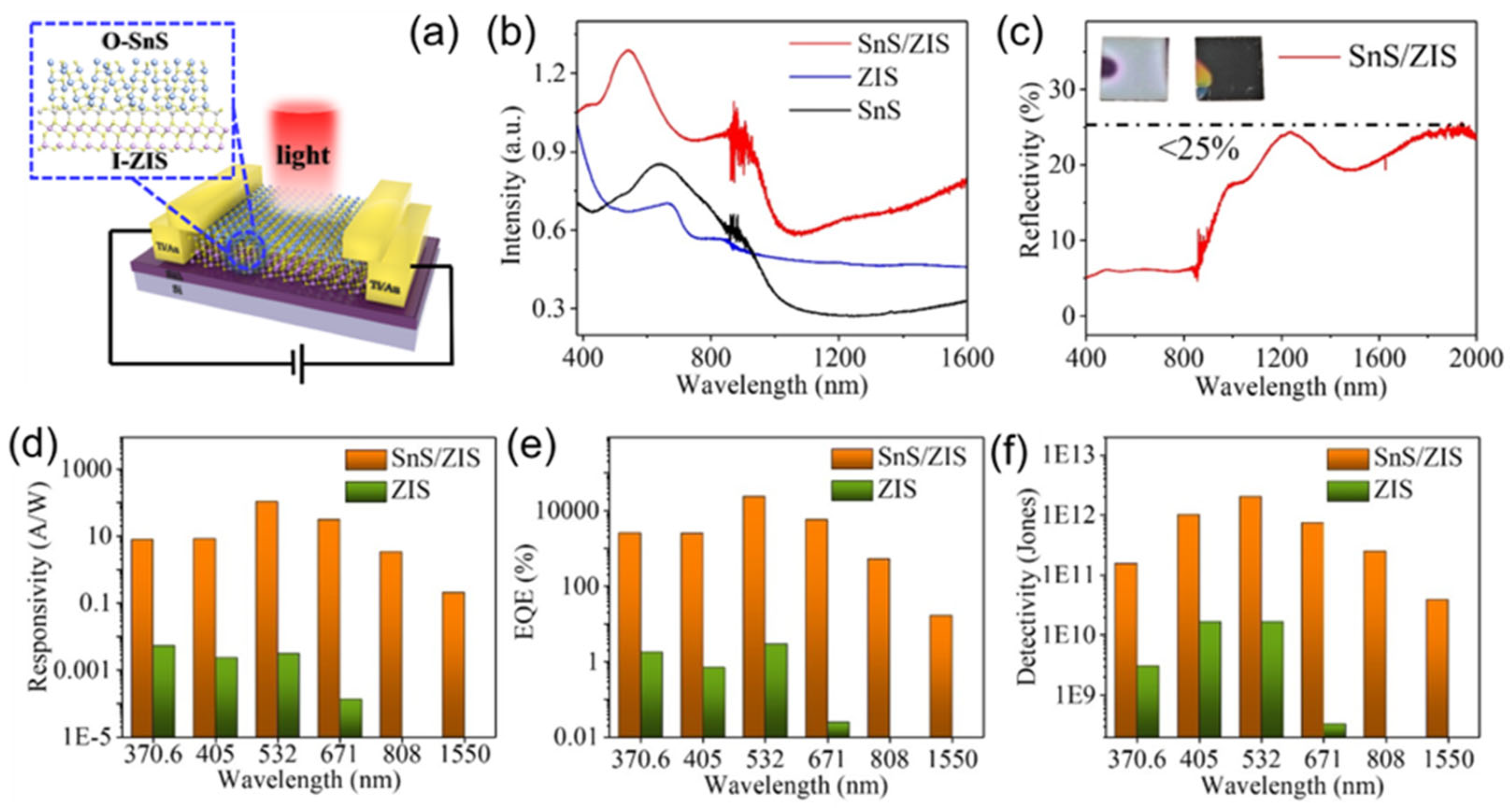
  162. Ye, Q.; Xu, D.; Cai, B.; Lu, J.; Yi, H.; Ma, C.; Zheng, Z.; Yao, J.; Ouyang, G.; Yang, G. High-performance hierarchical O-SnS/I-ZnIn2S4 photodetectors by leveraging the synergy of optical regulation and band tailoring. Mater. Horiz. 2022, 9, 2364–2375. [Google Scholar] [CrossRef]
  163. Xu, S.; Cheng, T.; Yan, Q.; Shen, C.; Yu, Y.; Lin, C.T.; Ding, F.; Zhang, J. Chloroform-Assisted Rapid Growth of Vertical Graphene Array and Its Application in Thermal Interface Materials. Adv. Sci. 2022, 9, 2200737. [Google Scholar] [CrossRef]
  164. Rahmati, B.; Hajzadeh, I.; Karimzadeh, R.; Mohseni, S.M. Facile, scalable and transfer free vertical-MoS2 nanostructures grown on Au/SiO2 patterned electrode for photodetector application. Appl. Surf. Sci. 2018, 455, 876–882. [Google Scholar] [CrossRef]
  165. Koçak, Y.; Gür, E. Growth Control of WS2: From 2D Layer by Layer to 3D Vertical Standing Nanowalls. ACS Appl. Mater. Interfaces 2020, 12, 15785–15792. [Google Scholar] [CrossRef]
  166. Fu, X.Y.; Zheng, Q.; Li, L.; Cao, M.S. Vertically implanting MoSe2 nanosheets on the RGO sheets towards excellent multi-band microwave absorption. Carbon 2022, 197, 324–333. [Google Scholar] [CrossRef]
  167. Guo, X.; Wang, S.; Yu, L.; Guo, C.; Yan, P.; Gao, H.; Liu, H. Dense SnS2 nanoplates vertically anchored on a graphene aerogel for pseudocapacitive sodium storage. Mater. Chem. Front. 2022, 6, 325–332. [Google Scholar] [CrossRef]
  168. Chen, Z.; Xiong, L.; Li, G.; Wei, L.; Yang, C.; Chen, M. Wafer-Scale Growth of Vertical-Structured SnSe2 Nanosheets for Highly Sensitive, Fast-Response UV–Vis–NIR Broadband Photodetectors. Adv. Opt. Mater. 2022, 10, 2102250. [Google Scholar] [CrossRef]
  169. Gao, Y.F.; Pang, S.M.; Bao, H.H.; Peng, X.Y.; Sun, Y.J.; Ren, S.L.; Meng, D.; Zhang, J. Growth mechanism for vertically oriented layered In2Se3 nanoplates. Phys. Rev. Mater. 2020, 4, 034002. [Google Scholar] [CrossRef]
  170. Han, S.S.; Kim, J.H.; Noh, C.; Kim, J.H.; Ji, E.; Kwon, J.; Yu, S.M.; Ko, T.J.; Okogbue, E.; Oh, K.H.; et al. Horizontal-to-Vertical Transition of 2D Layer Orientation in Low-Temperature Chemical Vapor Deposition-Grown PtSe2 and Its Influences on Electrical Properties and Device Applications. ACS Appl. Mater. Interfaces 2019, 11, 13598–13607. [Google Scholar] [CrossRef]
  171. Wu, Z.; Liu, G.; Wang, Y.; Yang, X.; Wei, T.; Wang, Q.; Liang, J.; Xu, N.; Li, Z.; Zhu, B.; et al. Seed-Induced Vertical Growth of 2D Bi2O2Se Nanoplates by Chemical Vapor Transport. Adv. Funct. Mater. 2019, 29, 1906639. [Google Scholar] [CrossRef]
  172. Peng, M.; Tao, Y.; Hong, X.; Liu, Y.; Wen, Z.; Sun, X. One-step synthesized PbSe nanocrystal inks decorated 2D MoS2 heterostructure for high stability photodetectors with photoresponse extending to near-infrared region. J. Mater. Chem. C 2022, 10, 2236–2244. [Google Scholar] [CrossRef]
  173. Zhang, Y.; Wang, F.; Zhao, X.; Feng, X.; Zhang, N.; Xia, F.; Ma, Y.; Li, H.; Zhai, T. 2D Ruddlesden–Popper perovskite sensitized SnP2S6 ultraviolet photodetector enabling high responsivity and fast speed. Nanoscale Horiz. 2023, 8, 108–117. [Google Scholar] [CrossRef] [PubMed]
  174. Carrano, J.C.; Grudowski, P.A.; Eiting, C.J.; Dupuis, R.D.; Campbell, J.C. Very low dark current metal–semiconductor–metal ultraviolet photodetectors fabricated on single-crystal GaN epitaxial layers. Appl. Phys. Lett. 1997, 70, 1992–1994. [Google Scholar] [CrossRef]
  175. Wei, Y.; Ren, Z.; Zhang, A.; Mao, P.; Li, H.; Zhong, X.; Li, W.; Yang, S.; Wang, J. Hybrid Organic/PbS Quantum Dot Bilayer Photodetector with Low Dark Current and High Detectivity. Adv. Funct. Mater. 2018, 28, 1706690. [Google Scholar] [CrossRef]
  176. Li, Z.; Xu, Y.; Zhang, J.; Cheng, Y.; Chen, D.; Feng, Q.; Xu, S.; Zhang, Y.; Zhang, J.; Hao, Y.; et al. Flexible Solar-Blind Ga2O3 Ultraviolet Photodetectors with High Responsivity and Photo-to-Dark Current Ratio. IEEE Photonics J. 2019, 11, 6803709. [Google Scholar] [CrossRef]
  177. Durairaj, S.; Ponnusamy, K.; Shinde, N.B.; Eswaran, S.K.; Asokan, V.; Park, J.B.; Chandramohan, S. Oxygen-Driven Growth Regulation and Defect Passivation in Chemical Vapor Deposited MoS2 Monolayers. Cryst. Growth Des. 2021, 21, 6793–6801. [Google Scholar] [CrossRef]
  178. Qiu, H.; Xu, T.; Wang, Z.; Ren, W.; Nan, H.; Ni, Z.; Chen, Q.; Yuan, S.; Miao, F.; Song, F.; et al. Hopping transport through defect-induced localized states in molybdenum disulphide. Nat. Commun. 2013, 4, 2642. [Google Scholar] [CrossRef]
  179. Greben, K.; Arora, S.; Harats, M.G.; Bolotin, K.I. Intrinsic and Extrinsic Defect-Related Excitons in TMDCs. Nano Lett. 2020, 20, 2544–2550. [Google Scholar] [CrossRef]
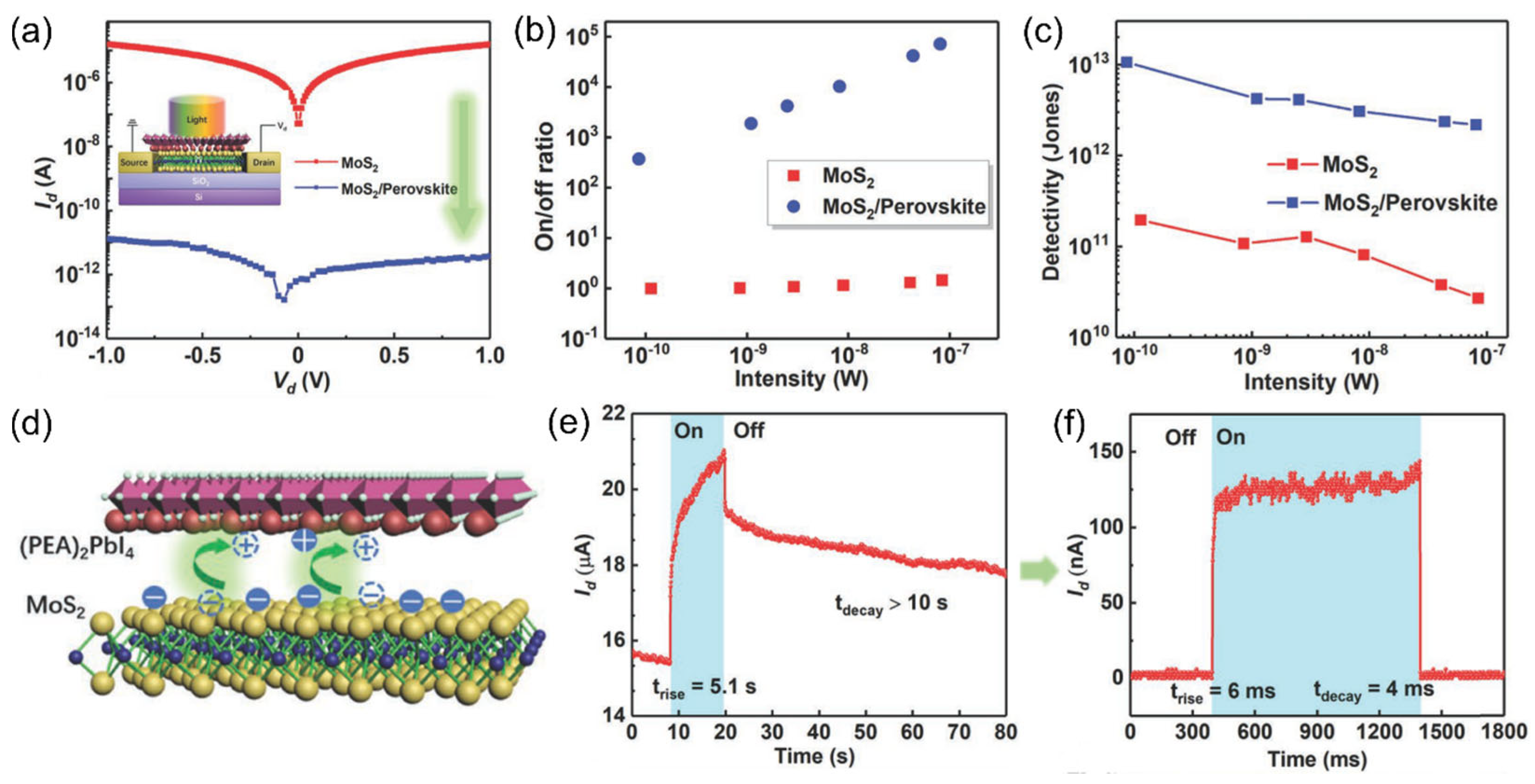
  180. Wang, H.; Wang, X.; Chen, Y.; Zhang, S.; Jiang, W.; Zhang, X.; Qin, J.; Wang, J.; Li, X.; Pan, Y.; et al. Extremely Low Dark Current MoS2 Photodetector via 2D Halide Perovskite as the Electron Reservoir. Adv. Opt. Mater. 2020, 8, 1901402. [Google Scholar] [CrossRef]
  181. Huang, M.; Wang, M.; Chen, C.; Ma, Z.; Li, X.; Han, J.; Wu, Y. Broadband Black-Phosphorus Photodetectors with High Responsivity. Adv. Mater. 2016, 28, 3481–3485. [Google Scholar] [CrossRef] [PubMed]
  182. Massicotte, M.; Schmidt, P.; Vialla, F.; Schädler, K.G.; Reserbat-Plantey, A.; Watanabe, K.; Taniguchi, T.; Tielrooij, K.J.; Koppens, F.H.L. Picosecond Photoresponse in van der Waals Heterostructures. Nat. Nanotechnol. 2016, 11, 42–46. [Google Scholar] [CrossRef] [PubMed]
  183. Fan, Y.; Zhou, Y.; Wang, X.; Tan, H.; Rong, Y.; Warner, J.H. Photoinduced Schottky Barrier Lowering in 2D Monolayer WS2 Photodetectors. Adv. Opt. Mater. 2016, 4, 1573–1581. [Google Scholar] [CrossRef]
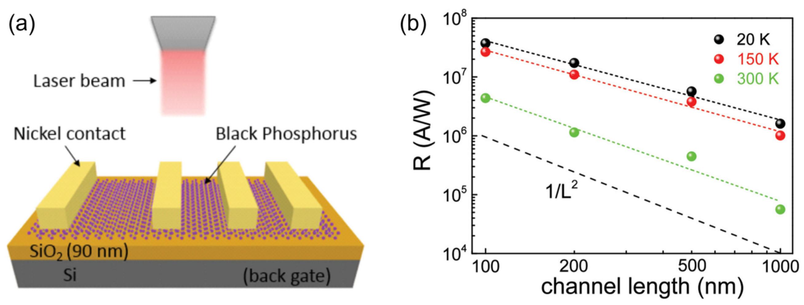
  184. Cao, Y.; Cai, K.; Hu, P.; Zhao, L.; Yan, T.; Luo, W.; Zhang, X.; Wu, X.; Wang, K.; Zheng, H. Strong enhancement of photoresponsivity with shrinking the electrodes spacing in few layer GaSe photodetectors. Sci. Rep. 2015, 5, 8130. [Google Scholar] [CrossRef] [PubMed]
  185. Yi, H.; Ma, C.; Wang, W.; Liang, H.; Cui, R.; Cao, W.; Yang, H.; Ma, Y.; Huang, W.; Zheng, Z.; et al. Quantum tailoring for polarization-discriminating Bi2S3 nanowire photodetectors and their multiplexing optical communication and imaging applications. Mater. Horiz. 2023, 10, 3369–3381. [Google Scholar] [CrossRef]
  186. Tsai, T.H.; Liang, Z.Y.; Lin, Y.C.; Wang, C.C.; Lin, K.I.; Suenaga, K.; Chiu, P.W. Photogating WS2 Photodetectors Using Embedded WSe2 Charge Puddles. ACS Nano 2020, 14, 4559–4566. [Google Scholar] [CrossRef] [PubMed]
  187. Ye, L.; Wang, P.; Luo, W.; Gong, F.; Liao, L.; Liu, T.; Tong, L.; Zang, J.; Xu, J.; Hu, W. Highly polarization sensitive infrared photodetector based on black phosphorus-on-WSe2 photogate vertical heterostructure. Nano Energy 2017, 37, 53–60. [Google Scholar] [CrossRef]
  188. Tang, X.; Huang, Y.; Cheng, K.; Yuan, Q.; Zou, J.; Li, C.; Ren, A.; Shen, K.; Wang, Z. Ultrasensitive WSe2/MoSe2 heterojunction photodetector enhanced by photogating effect. Microelectron. Eng. 2023, 274, 111980. [Google Scholar] [CrossRef]
  189. Qi, Z.; Yang, T.; Li, D.; Li, H.; Wang, X.; Zhang, X.; Li, F.; Zheng, W.; Fan, P.; Zhuang, X.; et al. High-responsivity two-dimensional p-PbI2/n-WS2 vertical heterostructure photodetectors enhanced by photogating effect. Mater. Horiz. 2019, 6, 1474–1480. [Google Scholar] [CrossRef]
  190. Ma, H.; Xing, Y.; Han, J.; Cui, B.; Lei, T.; Tu, H.; Guan, B.; Zeng, Z.; Zhang, B.; Lv, W. Ultrasensitive and Broad-Spectrum Photodetectors Based on InSe/ReS2 Heterostructure. Adv. Opt. Mater. 2022, 10, 2101772. [Google Scholar] [CrossRef]
  191. Zhang, X.L.; Li, J.; Leng, B.; Yang, L.; Song, Y.D.; Feng, S.Y.; Feng, L.Z.; Liu, Z.T.; Fu, Z.W.; Jiang, X.; et al. High-performance ultraviolet-visible photodetector with high sensitivity and fast response speed based on MoS2-on-ZnO photogating heterojunction. Tungsten 2023, 5, 91–99. [Google Scholar] [CrossRef]
  192. Yang, Y.; Li, J.; Choi, S.; Jeon, S.; Cho, J.H.; Lee, B.H.; Lee, S. High-responsivity PtSe2 photodetector enhanced by photogating effect. Appl. Phys. Lett. 2021, 118, 013103. [Google Scholar] [CrossRef]
  193. Hu, C.; Dong, D.; Yang, X.; Qiao, K.; Yang, D.; Deng, H.; Yuan, S.; Khan, J.; Lan, Y.; Song, H.; et al. Synergistic Effect of Hybrid PbS Quantum Dots/2D-WSe2 Toward High Performance and Broadband Phototransistors. Adv. Funct. Mater. 2017, 27, 1603605. [Google Scholar] [CrossRef]
  194. Duan, R.; Qi, W.; Li, P.; Tang, K.; Ru, G.; Liu, W. A High-Performance MoS2-Based Visible–Near-Infrared Photodetector from Gateless Photogating Effect Induced by Nickel Nanoparticles. Research 2023, 6, 0195. [Google Scholar] [CrossRef] [PubMed]
  195. Yu, Y.; Peng, M.; Zhong, F.; Wang, Z.; Ge, X.; Chen, H.; Guo, J.; Wang, Y.; Chen, Y.; Xu, T.; et al. Synergistic effects of extrinsic photoconduction and photogating in a short-wavelength ZrS3 infrared photodetector. Mater. Horiz. 2023, 10, 2579–2586. [Google Scholar] [CrossRef]
  196. Zandi, O.; Agrawal, A.; Shearer, A.B.; Reimnitz, L.C.; Dahlman, C.J.; Staller, C.M.; Milliron, D.J. Impacts of Surface Depletion on the Plasmonic Properties of Doped Semiconductor Nanocrystals. Nat. Mater. 2018, 17, 710–717. [Google Scholar] [CrossRef] [PubMed]
  197. Liu, Z.; Zhong, Y.; Shafei, I.; Borman, R.; Jeong, S.; Chen, J.; Losovyj, Y.; Gao, X.; Li, N.; Du, Y.; et al. Tuning infrared plasmon resonances in doped metal-oxide nanocrystals through cation-exchange reactions. Nat. Commun. 2019, 10, 1394. [Google Scholar] [CrossRef]
  198. Wang, M.; Yu, Y.; Prucnal, S.; Berencén, Y.; Shaikh, M.S.; Rebohle, L.; Khan, M.B.; Zviagin, V.; Hübner, R.; Pashkin, A.; et al. Mid- and far-infrared localized surface plasmon resonances in chalcogen-hyperdoped silicon. Nanoscale 2022, 14, 2826–2836. [Google Scholar] [CrossRef]
  199. Xie, C.; Lu, X.; Liang, Y.; Chen, H.; Wang, L.; Wu, C.; Wu, D.; Yang, W.; Luo, L. Patterned growth of β-Ga2O3 thin films for solar-blind deep-ultraviolet photodetectors array and optical imaging application. J. Mater. Sci. Technol. 2021, 72, 189–196. [Google Scholar] [CrossRef]
  200. Zhang, Y.; Cao, F.; Li, S.; Liu, X.; Kang, L.; Wu, L.; Fang, X. Integration of filter membrane and Ca2Nb3O10 nanosheets for high performance flexible UV photodetectors. J. Mater. Sci. Technol. 2022, 129, 108–114. [Google Scholar] [CrossRef]
  201. Deng, M.; Li, Z.; Deng, X.; Hu, Y.; Fang, X. Wafer-scale heterogeneous integration of self-powered lead-free metal halide UV photodetectors with ultrahigh stability and homogeneity. J. Mater. Sci. Technol. 2023, 164, 150–159. [Google Scholar] [CrossRef]
  202. Liu, S.; Yuan, X.; Zou, Y.; Sheng, Y.; Huang, C.; Zhang, E.; Ling, J.; Liu, Y.; Wang, W.; Zhang, C.; et al. Wafer-scale two-dimensional ferromagnetic Fe3GeTe2 thin films grown by molecular beam epitaxy. NPJ 2D Mater. Appl. 2017, 1, 30. [Google Scholar] [CrossRef]
  203. Xia, Y.; Ding, D.; Xiao, K.; Zhang, J.; Xu, S.; He, D.; Yue, X.; Rao, Q.; Wang, X.; Ding, S.; et al. Wafer-scale single-crystalline MoSe2 and WSe2 monolayers grown by molecular-beam epitaxy at low-temperature—The role of island-substrate interaction and surface steps. Nat. Sci. 2023, 3, 20220059. [Google Scholar] [CrossRef]
  204. Zhang, S.; Hao, Y.; Gao, F.; Wu, X.; Hao, S.; Qiu, M.; Zheng, X.; Wei, Y.; Hao, G. Controllable growth of wafer-scale two-dimensional WS2 with outstanding optoelectronic properties. 2D Mater. 2023, 11, 015007. [Google Scholar] [CrossRef]
  205. Wang, G.; Huang, J.; Zhang, S.; Meng, J.; Chen, J.; Shi, Y.; Jiang, J.; Li, J.; Cheng, Y.; Zeng, L.; et al. Wafer-Scale Single Crystal Hexagonal Boron Nitride Layers Grown by Submicron-Spacing Vapor Deposition. Small 2023, 19, 2301086. [Google Scholar] [CrossRef] [PubMed]
  206. Juvaid, M.M.; Ramachandra Rao, M.S. Wafer scale growth of MoS2 and WS2 by pulsed laser deposition. Mater. Today Proc. 2021, 35, 494–496. [Google Scholar] [CrossRef]
  207. Kim, D.H.; Park, J.C.; Park, J.; Cho, D.Y.; Kim, W.H.; Shong, B.; Ahn, J.H.; Park, T.J. Wafer-Scale Growth of a MoS2 Monolayer via One Cycle of Atomic Layer Deposition: An Adsorbate Control Method. Chem. Mater. 2021, 33, 4099–4105. [Google Scholar] [CrossRef]
  208. Fu, D.; Zhao, X.; Zhang, Y.Y.; Li, L.; Xu, H.; Jang, A.R.; Yoon, S.I.; Song, P.; Poh, S.M.; Ren, T.; et al. Molecular beam epitaxy of highly crystalline monolayer molybdenum disulfide on hexagonal boron nitride. J. Am. Chem. Soc. 2017, 139, 9392–9400. [Google Scholar] [CrossRef]
  209. Luo, G.; Shi, J.; Deng, W.; Chang, Z.; Lu, Z.; Zhang, Y.; Pan, R.; Jie, J.; Zhang, X.; Zhang, X. Boosting the Performance of Organic Photodetectors with a Solution-Processed Integration Circuit toward Ubiquitous Health Monitoring. Adv. Mater. 2023, 35, 2301020. [Google Scholar] [CrossRef]
  210. Gu, L.; Poddar, S.; Lin, Y.; Long, Z.; Zhang, D.; Zhang, Q.; Shu, L.; Qiu, X.; Kam, M.; Javey, A.; et al. A biomimetic eye with a hemispherical perovskite nanowire array retina. Nature 2020, 581, 278–282. [Google Scholar] [CrossRef]
  211. Zhang, L.; Li, N.; Ma, Q.; Ding, J.; Chen, C.; Hu, Z.; Zhao, W.; Li, Y.; Feng, H.; Li, M.; et al. Large-area flexible and transparent UV photodetector based on cross-linked Ag NW@ZnO NRs with high performance. J. Mater. Sci. Technol. 2022, 110, 65–72. [Google Scholar] [CrossRef]
  212. Ma, Y.; Ma, C.; Yi, H.; Liang, H.; Wang, W.; Zheng, Z.; Zou, Y.; Deng, Z.; Yao, J.; Yang, G. 1D Sb2S3 with Strong Mie Resonance Toward Highly-Sensitive Polarization-Discriminating Photodetection and Its Application in High-Temperature-Proof Imaging and Dual-Channel Communications. Adv. Opt. Mater. 2023. [Google Scholar] [CrossRef]
  213. Kong, L.; Li, G.; Su, Q.; Tan, X.; Zhang, X.; Liu, Z.; Liao, G.; Sun, B.; Shi, T. Polarization-Sensitive, Self-Powered, and Broadband Semimetal MoTe2/MoS2 van der Waals Heterojunction for Photodetection and Imaging. ACS Appl. Mater. Interfaces 2023, 15, 43135–43144. [Google Scholar] [CrossRef]
Figure 1. (a) Schematic diagram of the two-step fabrication of ZnIn2S4 nanofilms, including the pulsed-laser deposition and the post-growth high-temperature annealing. (b) X-ray diffraction patterns of ZnIn2S4 nanofilms before annealing (blue line) and after annealing (red line). The star symbols indicate the diffraction signals from the SiO2/Si substrate. (c) Schematic illustration of the healing of lattice defects of ZnIn2S4 nanofilm during the post-growth annealing processing. (d) Photoswitching curves of the photodetectors based on ZnIn2S4 nanofilms before annealing (blue line) and after annealing (red line). Reprinted with permission from Ref. [85]. Copyright 2022 Copyright Wiley-VCH (Wehenheim, Germany).
Materials 16 07372 g001
Figure 2. (a) Schematic diagram of the PDS-WSe2 photodetector. (b) Photocurrent of the pristine WSe2, SiO2/h-BN-WSe2, SiO2/Al2O3-WSe2, and SiO2/STO-WSe2 photodetectors as a function of light power density. (c) The response time and recovery time of pristine WSe2, SiO2/h-BN-WSe2, SiO2/Al2O3-WSe2, and SiO2/STO-WSe2 photodetectors. (d) Energy band diagram and carrier dynamics of PDS-2DLM upon illumination. Reprinted with permission from Ref. [112]. Copyright 2022 Copyright Wiley-VCH (Wehenheim, Germany).
Materials 16 07372 g002
Figure 3. (a) Schematic diagram of the WS2/Bi2Te3 photodetector. (b) Responsivity as a function of light power density of pristine WS2 photodetector and WS2/Bi2Te3 photodetectors with the thickness of the Bi2Te3 layer to be 2, 4, and 6 nm. Reprinted with permission from Ref. [116]. Copyright 2016, Royal Society of Chemical (London, UK). (c) Schematic diagram of the SiP2/SiO2 and SiP2/h-BN devices. The inset shows the corresponding optical microscopic image of the devices. (d) Cross-sectional TEM image showing the spacial distribution of the components. The inset shows the element mapping images of P, N, O, and Si. (e) IdsVds plots of the SiP2/SiO2 and SiP2/h-BN devices in the dark and under illumination. (f) Idst plots of the devices upon identical periodic illumination. Reprinted with permission from Ref. [117]. Copyright 2023 Copyright American Chemical Society (Washington, DC, USA).
Materials 16 07372 g003
Figure 4. (a) Schematic diagram of the Bi2Se3-WSe2-Bi2Se3 photodetector. (b) High-resolution cross-sectional TEM image of the Bi2Se3/WSe2 interface and the corresponding element mapping images of Bi, W, and Se elements. (c) I-V curves of the Bi2Se3-WSe2-Bi2Se3 and WSe2 devices in dark and under illumination with light intensity of 12.59 mW/cm2. (d) Power-density-dependent photocurrent density of the Bi2Se3-WSe2-Bi2Se3 and WSe2 devices. (e) Time-resolved photoresponse of the Bi2Se3-WSe2-Bi2Se3 device. Reprinted with permission from Ref. [129]. Copyright 2023 Copyright Wiley-VCH (Wehenheim, Germany).
Materials 16 07372 g004
Figure 5. (a) Schematic diagram of a monolayer MoS2 phototransistor modified with Ag nanodisks (AgNDs). (b) Reflection spectra of the bare SiO2/Si substrate (black line) and the AgNDs modified SiO2/Si substrate (blue line). The red line indicates the effect induced by the localized surface plasmon resonance effect from the AgNDs. (c) Spacial distribution of the light field intensity of the cross-section of a AgND on SiO2. (d) Responsivity as a function of wavelength of pristine MoS2 (black dots) and AgNDs/MoS2 (blue dots) photodetectors. Reprinted with permission from Ref. [144]. Copyright 2021 Copyright American Chemical Society (Washington, DC, USA).
Materials 16 07372 g005
Figure 6. (a) Schematic view of a metalens-integrated MoTe2 photodetector. (b) Schematic illustration of the light focusing by the Fresnel zone plate metalens integrated on the MoTe2 channel. Comparison of the (c) on/off ratio, (d) responsivity, EQE, and (e) detectivity between metalens/2H-MoTe2 photodetector and intrinsic 2H-MoTe2 photodetector under different power densities. Reprinted with permission from Ref. [154]. Copyright 2022 Copyright Wiley-VCH (Wehenheim, Germany).
Materials 16 07372 g006
Figure 7. (a) Schematic diagram of a V-SnS/I-ZnIn2S4 photodetector. (b) Absorption spectra of the PLD-derived SnS/ZnIn2S4 (red line), ZnIn2S4 (blue line), and SnS (black line) nanofilms. (c) Reflection spectrum of the PLD-derived SnS/ZnIn2S4 nanofilm. The digital images of SnS (left) and SnS/ZnIn2S4 (right) nanofilms are shown in the inset. (df) Summary of responsivity, EQE, and detectivity of the ZnIn2S4 (green columns) and SnS/ZnIn2S4 (orange columns) photodetectors upon illumination with various wavelengths. Reprinted with permission from Ref. [162]. Copyright 2022, Royal Society of Chemical (London, UK).
Materials 16 07372 g007
Figure 8. (a) I-V curves of the pristine MoS2 device (red line) and the MoS2/(PEA)2PbI4 hybrid PwER device (blue line). The inset shows the schematic diagram of the side view of device structure. (b) On/off ratio and (c) detectivity as a function of light power of the MoS2 device (red dots) and the MoS2/(PEA)2PbI4 hybrid device (blue dots). (d) Schematic illustration of the electron transfer process at the MoS2/(PEA)2PbI4 interface. (e,f) A single photoswithcing curve of the MoS2 device and the MoS2/(PEA)2PbI4 hybrid device, respectively. Reprinted with permission from Ref. [180]. Copyright 2020 Copyright Wiley-VCH (Wehenheim, Germany).
Materials 16 07372 g008
Figure 9. (a) Schematic illustration of lateral black phosphorus photodetectors with various channel lengths. (b) Responsivity as a function of channel length of black phosphorus photodetectors. Reprinted with permission from Ref. [181]. Copyright 2016 Copyright Wiley-VCH (Wehenheim, Germany).
Materials 16 07372 g009
Figure 10. (a) Schematic diagram of a WS2/WSe2 photodetector. (b) I–V curves of the WS2 photodetector (triangles) and WS2/WSe2 photodetector (circles) in dark and under illumination. (c) Energy band diagram illustrating the carrier dynamics of the WS2/WSe2 photodetector. Reprinted with permission from Ref. [186]. Copyright 2022 Copyright American Chemical Society (Washington, DC, USA).
Materials 16 07372 g010
Disclaimer/Publisher’s Note: The statements, opinions and data contained in all publications are solely those of the individual author(s) and contributor(s) and not of MDPI and/or the editor(s). MDPI and/or the editor(s) disclaim responsibility for any injury to people or property resulting from any ideas, methods, instructions or products referred to in the content.

