
First-Principles Study of Adsorption of Pb Atoms on 3C-SiC


Abstract
:1. Introduction
2. Method
3. Results
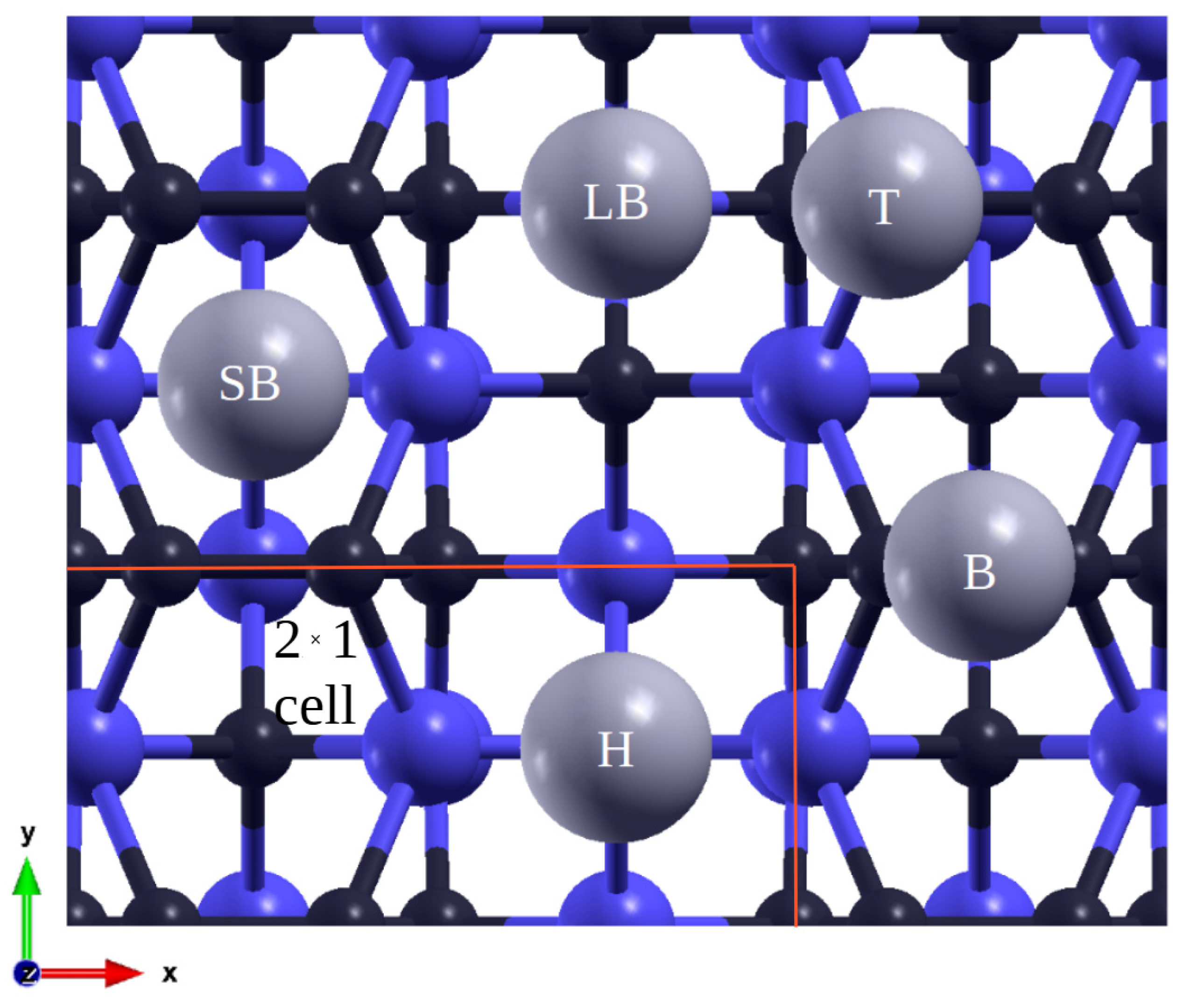
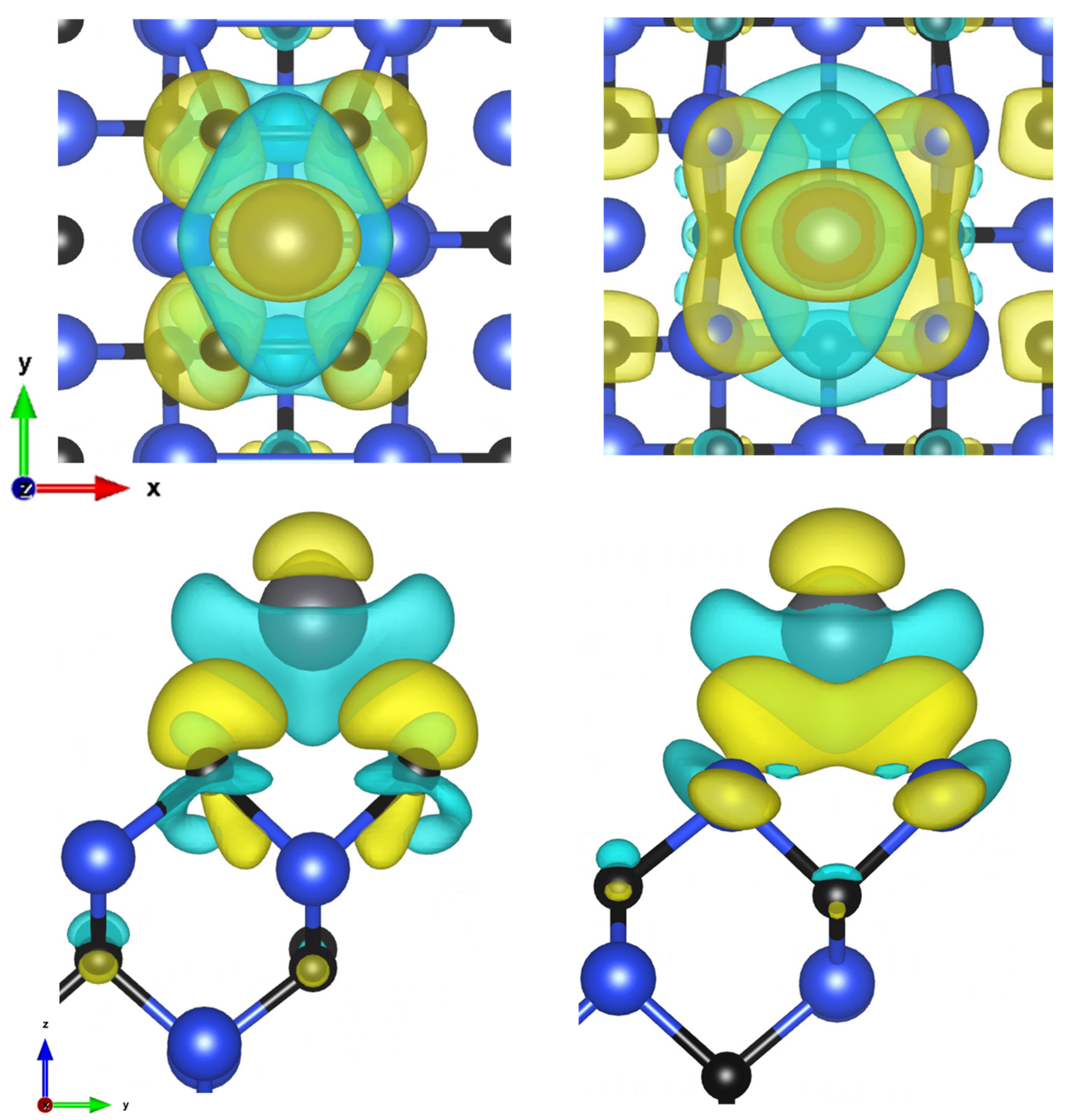
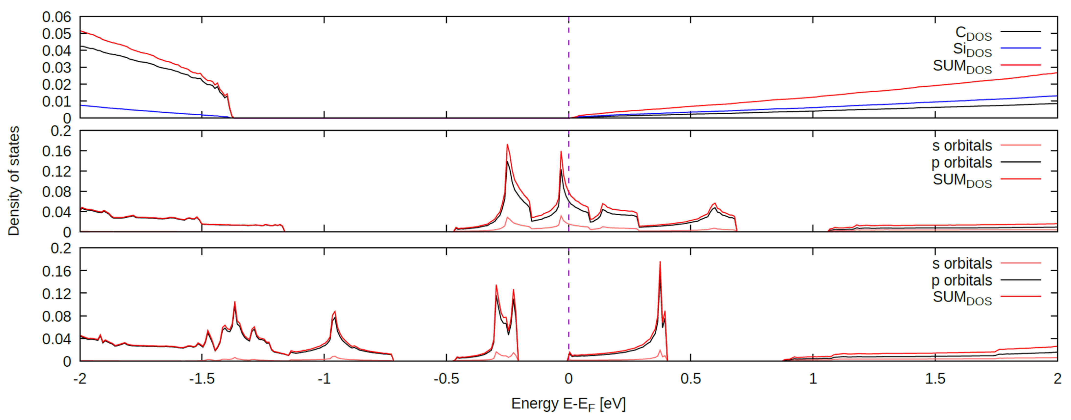
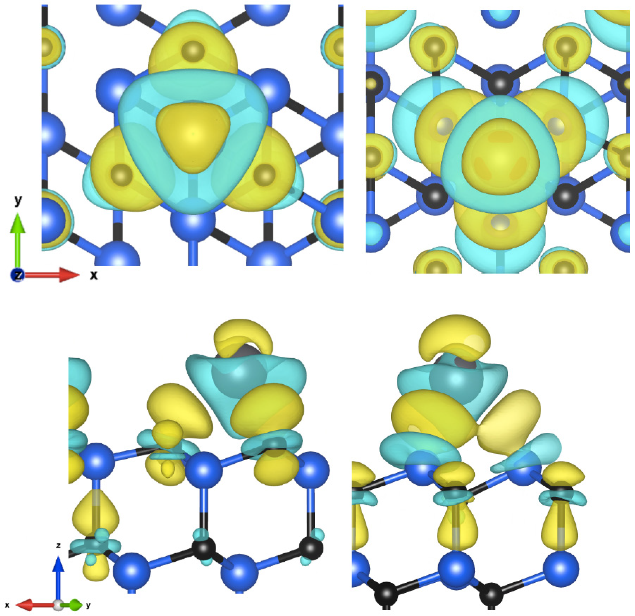
3.1. (100) Surface
3.2. (110) Surface
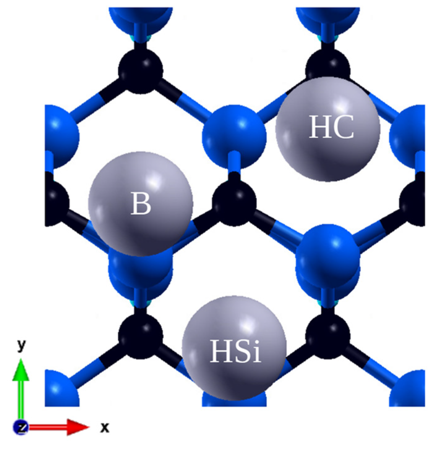
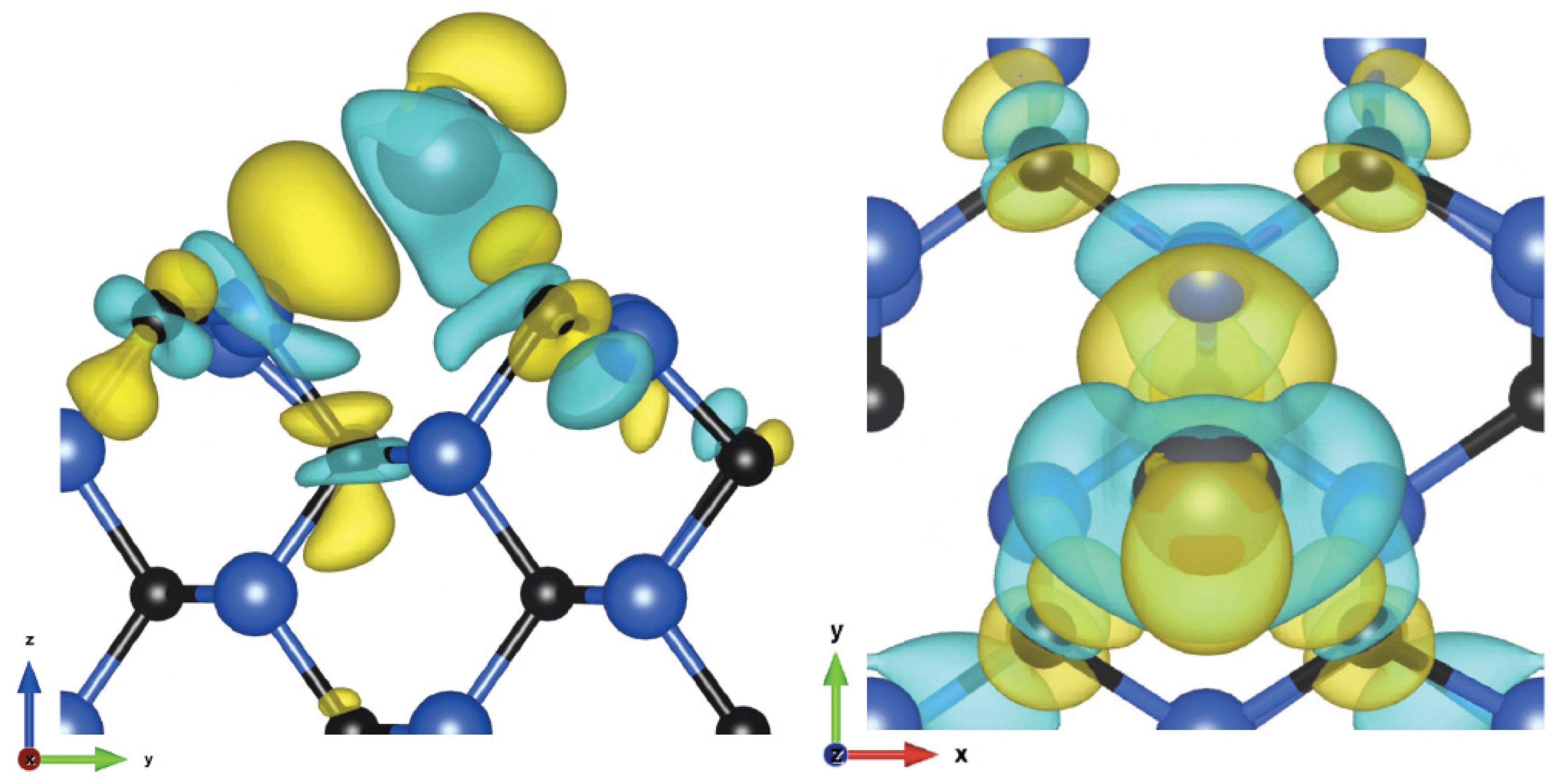
3.3. (111) Surface
4. Discussion and Conclusions
Author Contributions
Funding
Conflicts of Interest
References
- Aristov, V.Y. β-SiC (100) surface: Atomic structures and electronic properties. Phys.-Uspekhi 2001, 44, 761–783. [Google Scholar] [CrossRef]
- Cheng, E.T.; Garner, J.K.; Simnad, M.; Talbot, J. A low-activation fusion blanket with SiC structure and Pb-Li breeder. Fusion Eng. Des. 1994, 28, 335–340. [Google Scholar]
- Huke, A.; Ruprecht, G.; Weißbach, D.; Gottlieb, S.; Hussein, A.; Czerski, K. The Dual Fluid Reactor—A novel concept for a fast nuclear reactor of high efficiency. Ann. Nucl. Energy 2015, 80, 225–235. [Google Scholar] [CrossRef]
- Kim, W.J.; Park, J.N.; Cho, M.S.; Park, J.Y. Effect of coating temperature on properties of the SiC layer in TRISO-coated particles. J. Nucl. Mater. 2009, 392, 213–218. [Google Scholar] [CrossRef]
- Wei, D.; Sierchuła, J.; Dąbrowski, M.P.; Czerski, K.; Ruprecht, G. Dual Fluid Reactor as a long-term burner of actinides in spent nuclear fuel. Int. J. Energy Res. 2021, 45, 11589–11597. [Google Scholar]
- Miao, Y.; Mo, K.; Fei, T.; Cao, Y. Multiphysics simulations of Self-Regulating performance of an optimized molten metal fuel microreactor design. Nucl. Eng. Des. 2023, 406, 112244. [Google Scholar] [CrossRef]
- Lei, Y.; Zhang, Y.; Li, X.; Xu, Y.; Wu, X.; Sun, M.; Li, B.; Liu, C.; Wang, Z. Simulation and experimental studies of the dissolution corrosion of 4H-SiC in liquid Pb/Bi. Appl. Surf. Sci. 2022, 585, 152686. [Google Scholar] [CrossRef]
- Rosso, E.F.; Baierle, R.J. First principles study about Fe adsorption on planar SiC nanostructures: Monolayer and nanoribbon. Microelectron. Eng. 2014, 126, 37–41. [Google Scholar] [CrossRef]
- Pourreza, N.; Naghdi, T. Silicon carbide nanoparticles as an adsorbent for solid phase extraction of lead and determination by flame atomic absorption spectrometry. J. Ind. Eng. Chem. 2014, 20, 3502–3506. [Google Scholar] [CrossRef]
- Pollmann, J.; Kruger, P. Reconstruction models of cubic SiC surfaces. J. Phys. Condens. Matter 2004, 16, 1659–1703. [Google Scholar] [CrossRef]
- Daviau, K.; Lee, K.K.M. High-Pressure, High-Temperature Behavior of Silicon Carbide: A Review. Crystals 2018, 8, 217. [Google Scholar] [CrossRef]
- Giannozzi, P.; Baroni, S.; Bonini, N.; Calandra, M.; Car, R.; Cavazzoni, C.; Ceresoli, D.; Chiarotti, G.L.; Cococcioni, M.; Dabo, I.; et al. QUANTUM ESPRESSO: A modular and open-source software project for quantum simulations of materials. J. Phys. Condens. Matter 2009, 21, 395502. [Google Scholar] [CrossRef] [PubMed]
- Giannozzi, P.; Andreussi, O.; Brumme, T.; Bunau, O.; Nardelli, M.B.; Calandra, M.; Car, R.; Cavazzoni, C.; Ceresoli, D.; Cococcioni, M.; et al. Advanced capabilities for materials modelling with Quantum ESPRESSO. J. Phys. Condens. Matter 2017, 29, 465901. [Google Scholar] [CrossRef] [PubMed]
- We Used the Pseudopotentials: C.pbe-n-kjpaw_psl.1.0.0.UPF Si.pbe-nl-kjpaw_psl.1.0.0.UPF H.pbe-kjpaw.UPF Pb.rel-pbe-dn-kjpaw_psl.1.0.0.UPF. Available online: http://www.quantum-espresso.org (accessed on 10 October 2022).
- Perdew, J.P.; Burke, K.; Ernzerhof, M. Generalized Gradient Approximation Made Simple. Phys. Rev. Lett. 1997, 78, 1396. [Google Scholar] [CrossRef]
- Visikovskiy, A.; Hayashi, S.; Kajiwara, T.; Komori, F.; Yaji, K.; Tanaka, S. Computational study of heavy group IV elements (Ge, Sn, Pb) triangular lattice atomic layers on SiC (0001) surface. arXiv 2018, arXiv:1809.00829. [Google Scholar]
- Mashhadzadeh, A.H.; Ahangari, M.G.; Salmankhani, A.; Fataliyan, M. Density functional theory study of adsorption properties of non-carbon, carbon and functionalized graphene surfaces towards the zinc and lead atoms. Physica E 2018, 104, 275–285. [Google Scholar] [CrossRef]
- Murnaghan, F.D. The Compressibility of Media under Extreme Pressures. Proc. Natl. Acad. Sci. USA 1944, 30, 244–247. [Google Scholar] [CrossRef]
- Lee, W.H.; Yao, X.H. First principle investigation of phase transition and thermodynamic properties of SiC. Comput. Mater. Sci. 2015, 106, 76–82. [Google Scholar] [CrossRef]
- Braekken, H. Zur Kristallstruktur des kubischen Karborunds. Z. Krist. 1977, 75, 572–573. [Google Scholar]
- Momma, K.; Izumi, F. VESTA 3 for three-dimensional visualization of crystal, volumetric and morphology data. J. Appl. Crystallogr. 2011, 44, 1272–1276. [Google Scholar] [CrossRef]
- Hirel, P. Atomsk: A tool for manipulating and converting atomic data files. Comput. Phys. Commun. 2015, 197, 212–219. [Google Scholar] [CrossRef]
- Bader, R.F.W. Atoms in molecules. Acc. Chem. Res. 1985, 18, 9–15. [Google Scholar] [CrossRef]
- Wang, W.; Li, C.; Cao, J.; Fang, C. Adsorption behaviors of cobalt on the graphite and SiC surface: A first-principles study. Sci. Technol. Nucl. Install. 2017, 2017, 8296387. [Google Scholar] [CrossRef]
- Konopka, A.; Aşik, B.; Gerstmann, U.; Rauls, E.; Vollmers, N.J.; Rohrmüller, M.; Schmidt, W.G.; Friedel, B.; Greulich-Weber, S. Paramagnetic signature of microcrystalline silicon carbide. IOP Conf. Ser. Mater. Sci. Eng. 2010, 15, 012013. [Google Scholar] [CrossRef]
- Catellani, A.; Galli, G.; Gygi, F. Reconstruction and thermal stability of the cubic SiC (001) surfaces. Phys. Rev. Lett. 1996, 77, 5090. [Google Scholar] [CrossRef]
- Catellani, A.; Cicero, G. Modifications of cubic SiC surfaces studied by ab initio simulations: From gas adsorption to organic functionalization. J. Phys. D Appl. Phys. 2007, 40, 6215–6224. [Google Scholar] [CrossRef]
- Abavare, E.K.K.; Iwata, J.; Yaya, A. Surface energy of Si (110)-and 3C-SiC (111)-terminated surfaces. Phys. Status Solidi B 2014, 251, 1408–1415. [Google Scholar] [CrossRef]
- Liu, X.T.; Hu, T.W.; Miao, Y.P.; Ma, D.Y.; Chu, P.K.; Ma, F.; Xu, K.W. Selective growth of Pb islands on graphene/SiC buffer layers. J. Appl. Phys. 2015, 117, 065304. [Google Scholar] [CrossRef]
- Yurtsever, A.; Onoda, J.; Iimori, T.; Niki, K.; Miyamachi, T.; Abe, M.; Mizuno, S.; Tanaka, S.; Komori, F.; Sugimoto, Y. Effects of Pb intercalation on the structural and electronic properties of epitaxial graphene on SiC. Small 2016, 12, 3956–3966. [Google Scholar] [CrossRef]
- Chen, S.; Thiel, P.A.; Conrad, E.; Tringides, M.C. Growth and stability of Pb intercalated phases under graphene on SiC. Phys. Rev. Mater. 2020, 4, 124005. [Google Scholar] [CrossRef]
- Li, L.; Tsong, I.S.T. Atomic structures of 6H-SiC (0001) and (0001-) surfaces. Surf. Sci. 1995, 351, 141–148. [Google Scholar] [CrossRef]
- Tunison, H. Compatibility of SiC and SiC Composites with Molten Lead; KAPL: Niskayuna, NY, USA, 2006. [Google Scholar]
- Liu, G.W.; Muolo, M.L.; Valenza, F.; Passerone, A. Survey on wetting of SiC by molten metals. Ceram. Int. 2010, 36, 1177–1188. [Google Scholar] [CrossRef]
- Gordy, W.; Thomas, W.J.O. Electronegativity values from thermochemical data. J. Chem. Phys. J. Chem. Phys. 1961, 24, 439–444. [Google Scholar]
- Kuganathan, N.; Anurakavan, S.; Abiman, P.; Iyngaran, P.; Gkanas, E.I.; Chroneos, A. Adsorption of lead on the surfaces of pristine and B, Si and N-doped graphene. Phys. B 2021, 600, 412639. [Google Scholar] [CrossRef]
- Wachowicz, E.; Sznajder, M.; Majewski, J.A. Ab initio studies of Al and Ga adsorption on 4H-SiC {0001} surfaces. Acta Phys. Pol. A 2012, 122, 1045–1048. [Google Scholar] [CrossRef]
- Filimonov, S.N. Ab Initio Calculations of Absolute Surface Energies of Clean and Hydrogen Covered 3C-SiC(001), (110) and (111) Surfaces. Mater. Sci. Forum 2015, 821–823, 363–366. [Google Scholar]
- Taylor, C.D.; Ke, H. Investigation of the intrinsic corrosion and hydrogen susceptibility of metals and alloys using density functional theory. Corros. Rev. 2021, 39, 177–209. [Google Scholar] [CrossRef]


| Adsorption Site | 1/16 ML | 1/4 ML | 1/2 ML | 3/4 ML |
|---|---|---|---|---|
| Short bridge (SB) | −2.33 | −2.15 | ||
| Long bridge (LB) | −2.09 | −2.16 | −2.16 | −2.04 |
| Bridge (B) | −1.92 | −1.83 | −2.16 | |
| Hollow (H) | −2.05 | −2.23 |
| Adsorption Site | 1/16 ML | 1/4 ML | 1/2 ML | 3/4 ML |
|---|---|---|---|---|
| Short bridge (SB) | −2.53 | −2.19 | ||
| Top (T) | −1.09 | |||
| Bridge (B) | −2.23 | −1.88 | −2.24 | −1.83 |
| Adsorption Site | 1/18 ML | 1/8 ML | 1/4 ML | 3/8 ML | 1/2 ML |
|---|---|---|---|---|---|
| Hollow Si (HSi) | −2.05 | −1.99 | |||
| Hollow C (HC) | −2.36 | −2.34 | −2.81 | −2.46 | −2.34 |
| Adsorption Site | 1/9 ML | 1/4 ML | 1/2 ML | 3/4 ML | 1 ML |
|---|---|---|---|---|---|
| Top (T) | −2.65 | −2.56 | −3.02 | −2.72 | −2.39 |
| fcc Hollow | −3.51 | −3.39 | −2.72 | −2.39 | |
| hcp Hollow | −3.64 | −3.59 | −3.02 | −2.72 | −2.39 |
| Adsorption Site | 1/9 ML | 1/4 ML | 1/2 ML | 3/4 ML | 1 ML |
|---|---|---|---|---|---|
| Top (T) | −2.71 | −2.43 | −2.93 | −2.77 | −2.36 |
| fcc Hollow | −3.6 | −3.53 | |||
| hcp Hollow | −3.49 | −3.45 | −2.93 | −2.77 | −2.36 |
Disclaimer/Publisher’s Note: The statements, opinions and data contained in all publications are solely those of the individual author(s) and contributor(s) and not of MDPI and/or the editor(s). MDPI and/or the editor(s) disclaim responsibility for any injury to people or property resulting from any ideas, methods, instructions or products referred to in the content. |
© 2023 by the authors. Licensee MDPI, Basel, Switzerland. This article is an open access article distributed under the terms and conditions of the Creative Commons Attribution (CC BY) license (https://creativecommons.org/licenses/by/4.0/).
Share and Cite
Komorowicz, M.; Skrobas, K.; Czerski, K. First-Principles Study of Adsorption of Pb Atoms on 3C-SiC. Materials 2023, 16, 6700. https://doi.org/10.3390/ma16206700
Komorowicz M, Skrobas K, Czerski K. First-Principles Study of Adsorption of Pb Atoms on 3C-SiC. Materials. 2023; 16(20):6700. https://doi.org/10.3390/ma16206700
Chicago/Turabian StyleKomorowicz, Michal, Kazimierz Skrobas, and Konrad Czerski. 2023. "First-Principles Study of Adsorption of Pb Atoms on 3C-SiC" Materials 16, no. 20: 6700. https://doi.org/10.3390/ma16206700
APA StyleKomorowicz, M., Skrobas, K., & Czerski, K. (2023). First-Principles Study of Adsorption of Pb Atoms on 3C-SiC. Materials, 16(20), 6700. https://doi.org/10.3390/ma16206700