
Distribution of Hydrogen and Defects in the Zr/Nb Nanoscale Multilayer Coatings after Proton Irradiation

 ,
,  , , , , , and
Abstract
:1. Introduction
2. Materials and Methods
3. Results and Discussion
4. Conclusions
- (1)
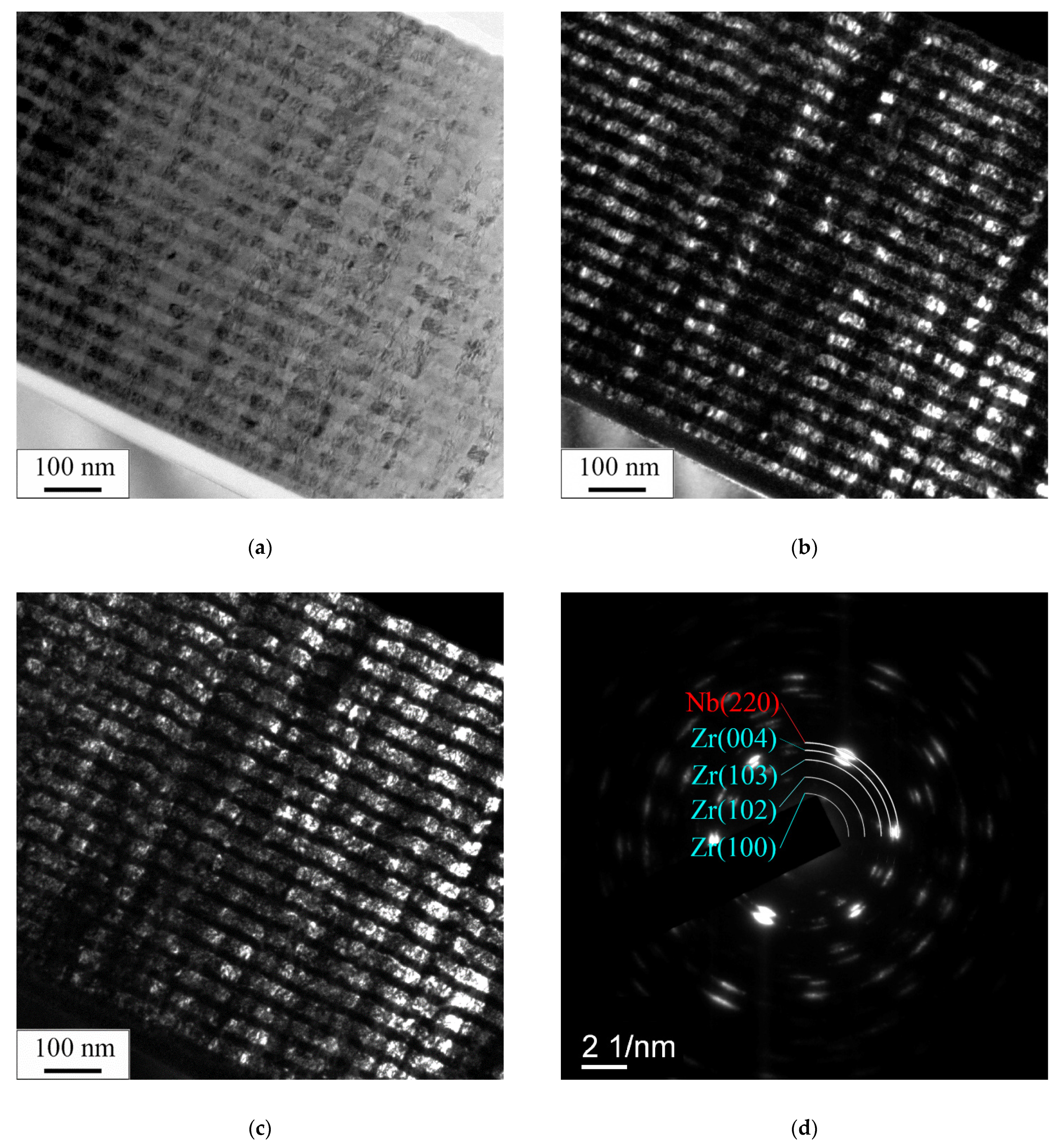
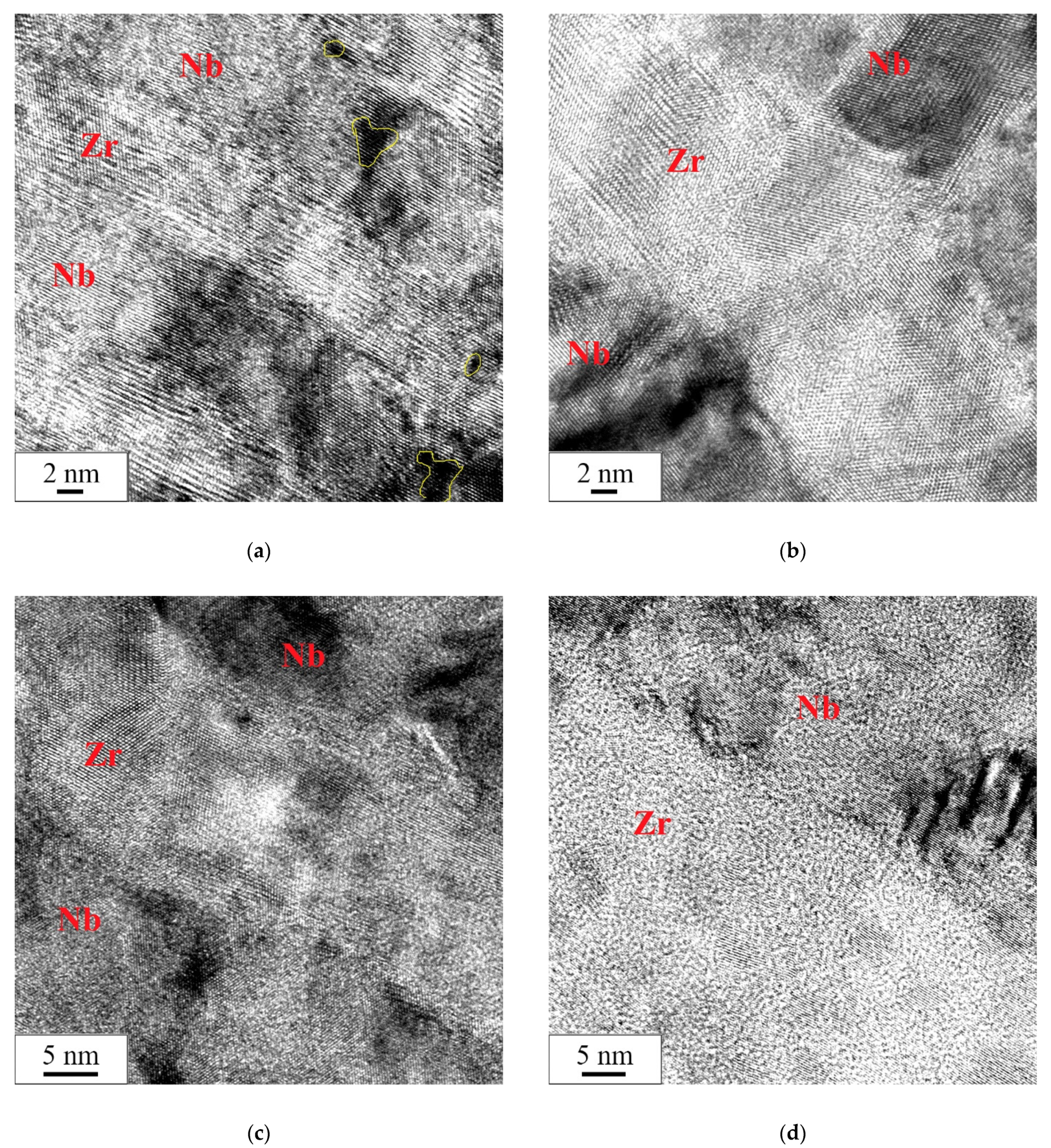
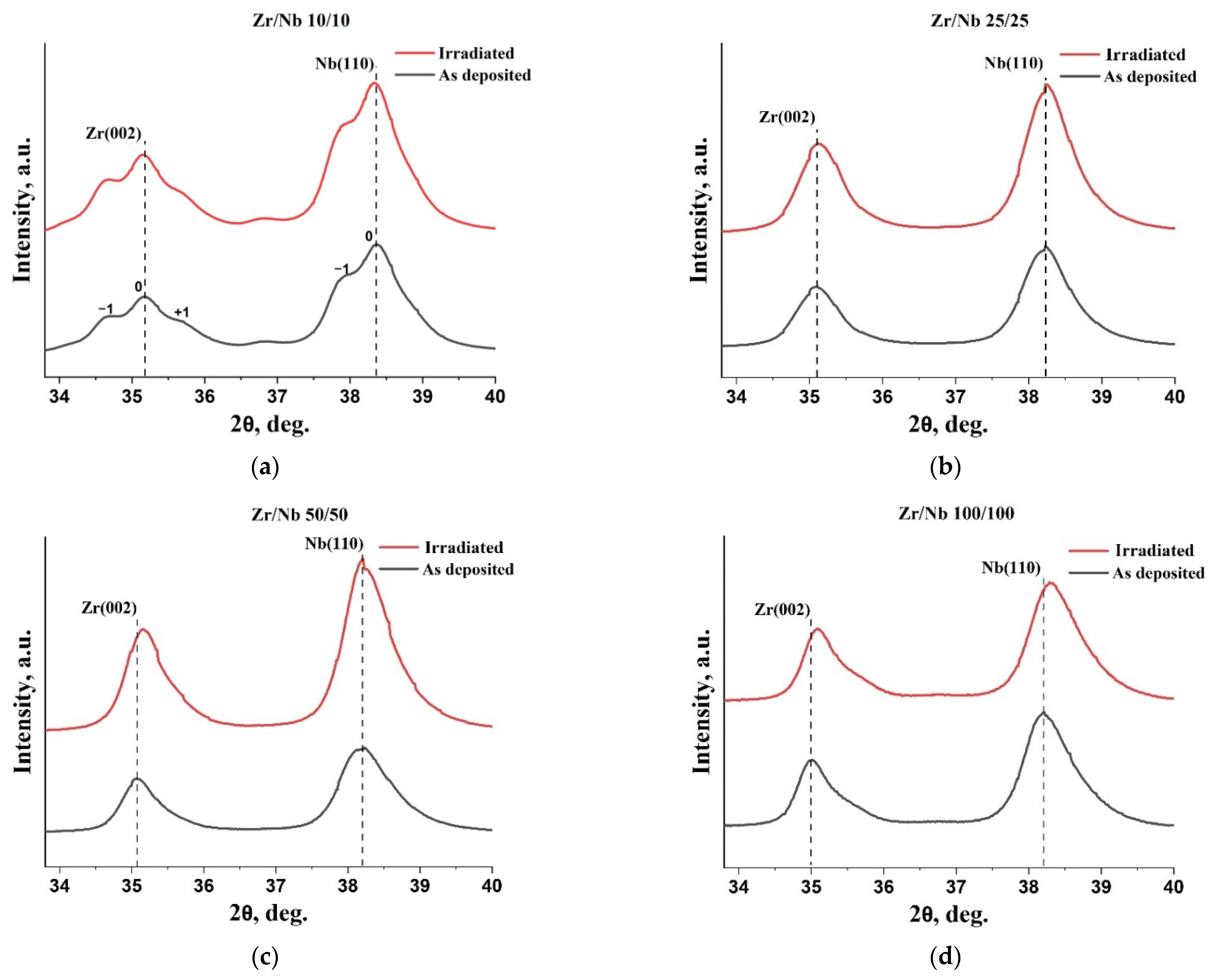
- Irradiation at the studied doses did not affect the crystal structure and grain orientation inside the Zr and Nb layers. A feature of the samples with a thickness of individual Zr/Nb layers of 10 nm was the presence of nanovoids consisting of several vacant atomic positions. After irradiation, slight changes in the diffraction pattern were noted for Zr/Nb NMCs with a separate layer thickness of 50 and 100 nm. The shift in the diffraction peak in irradiated metal multilayers was caused by the crystal lattice distortions and stresses arising in the layers.
- (2)
- An increase in the thickness of alternating Zr/Nb multilayers from 25 to 100 nm led to a significant decrease in the nanohardness values of the samples, compared with NMC samples with a thickness of individual Zr/Nb layers of 10 nm. Proton irradiation at the studied parameters led to a decrease in the values of nanohardness of the Zr/Nb NMCs. Meanwhile, irradiation with protons did not affect the values of Young’s modulus.
- (3)
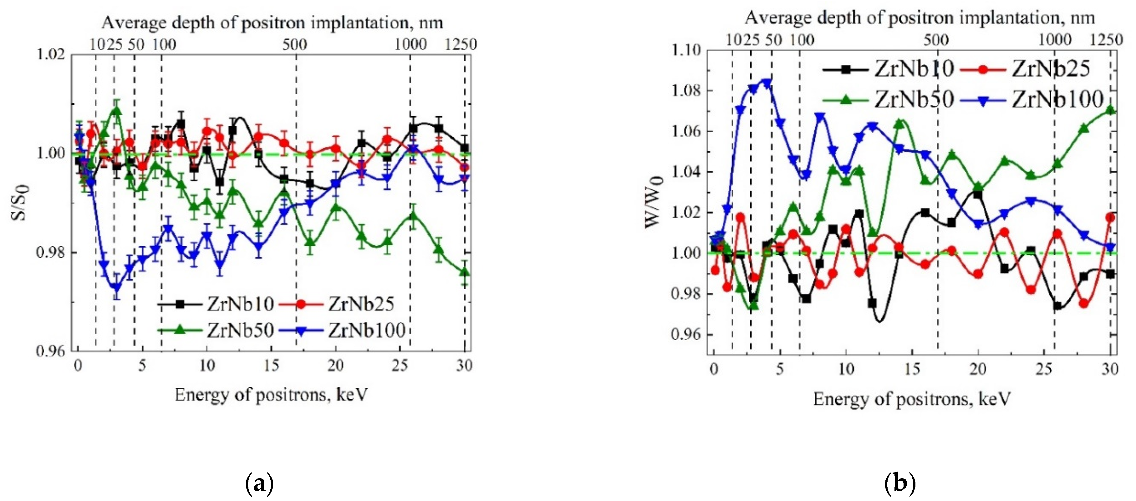
- The layer-by-layer analysis by DBS using a variable-energy positron beam did not reveal the additional defects in NMC Zr/Nb after proton irradiation. The S parameter remained unchanged or decreased.
- (4)
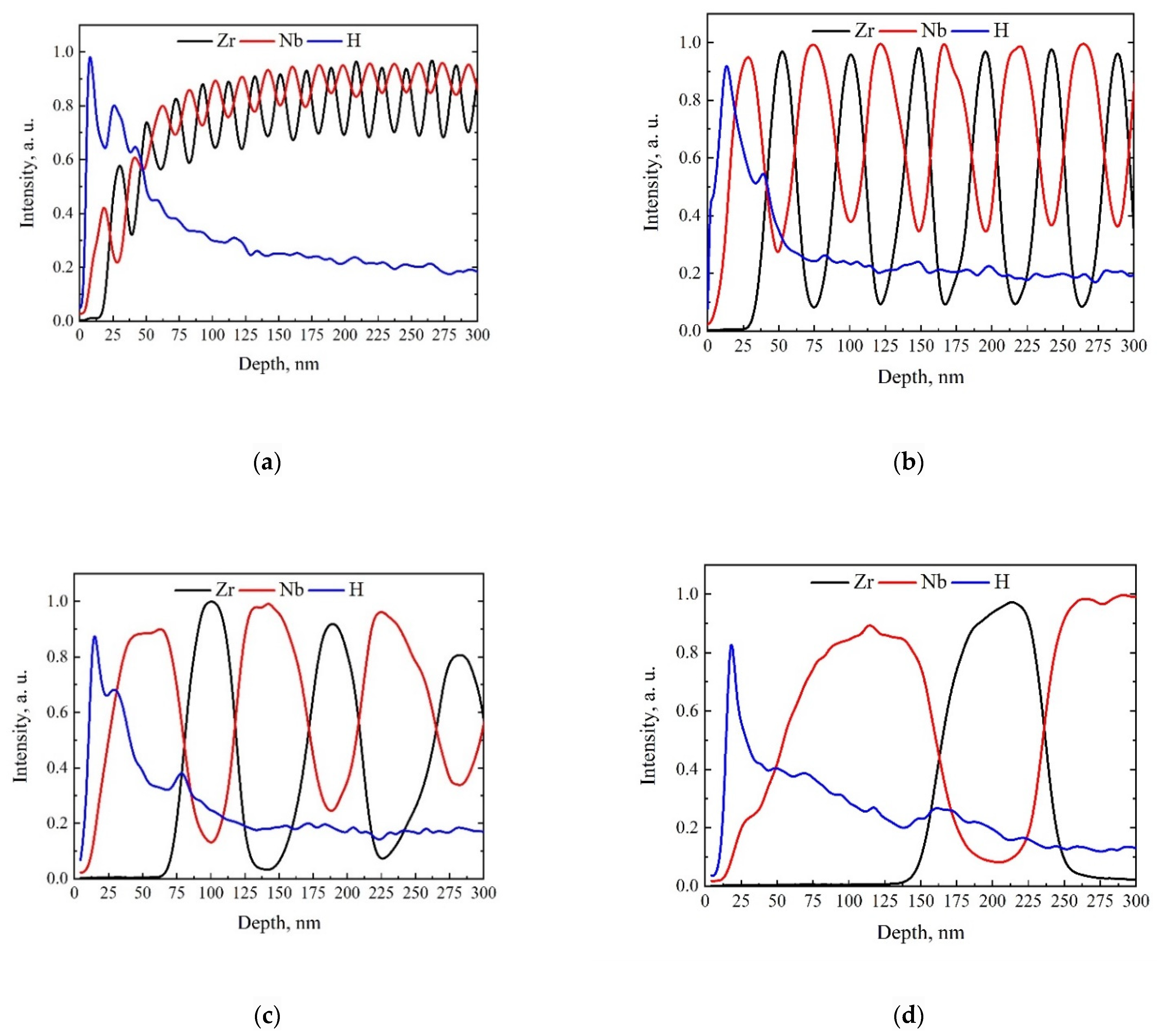
- The irregular H accumulation at the interfaces in NMC Zr/Nb after proton irradiation was observed; H accumulated at the Nb/Zr interface much more than at the Zr/Nb interface possibly due to significant differences in H diffusion barriers in the bulk of Zr and Nb multilayers, as well as near the interface’s region.
- (5)
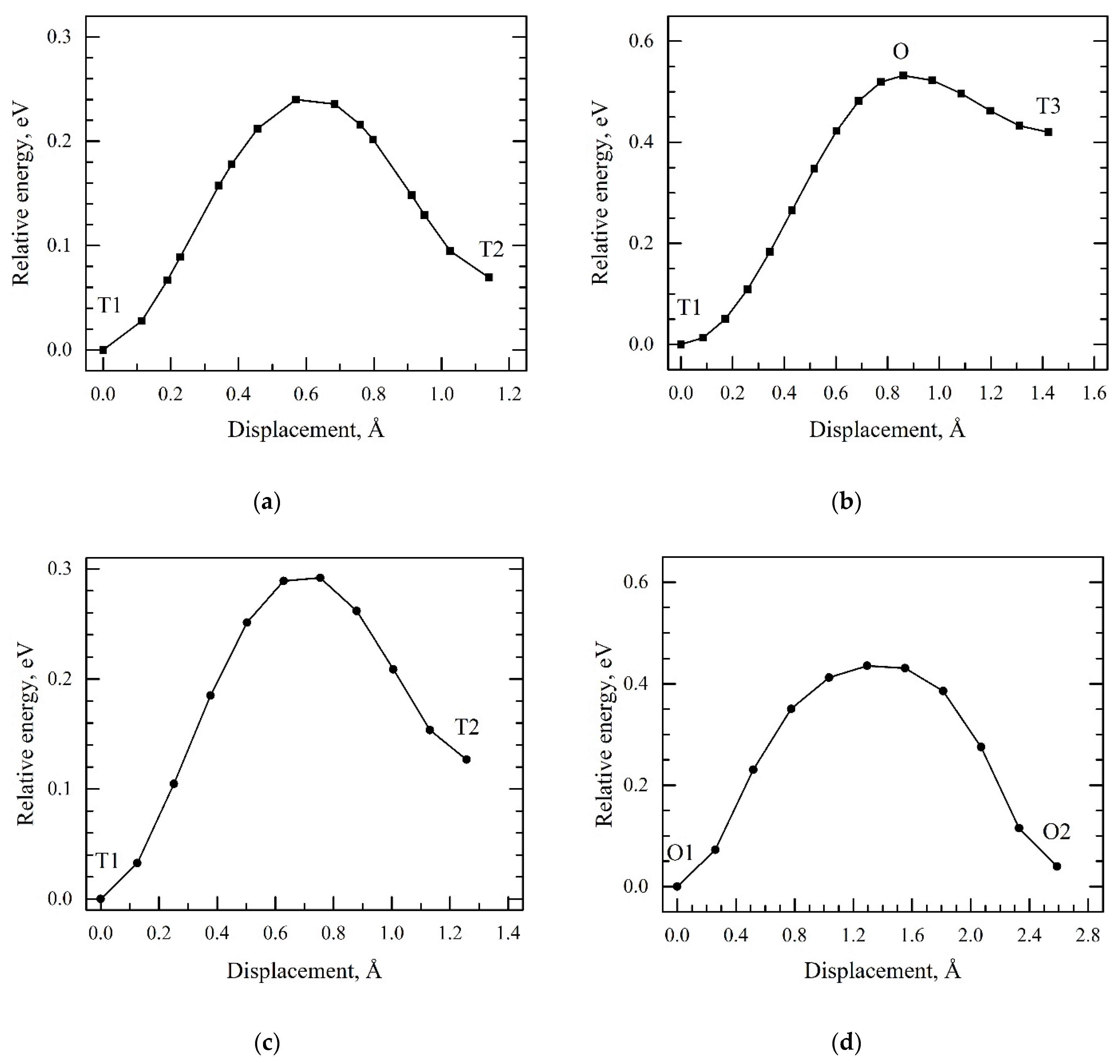
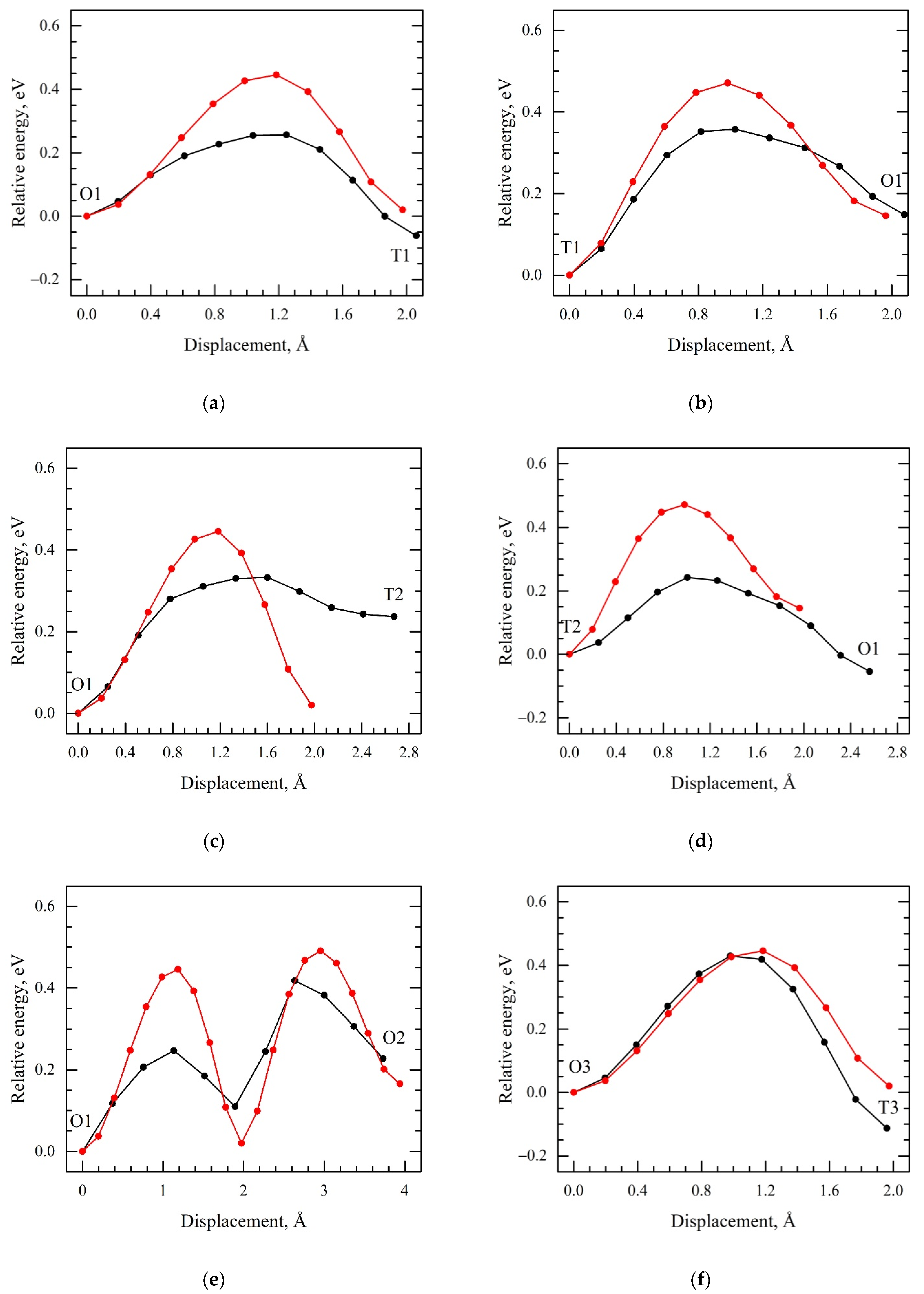
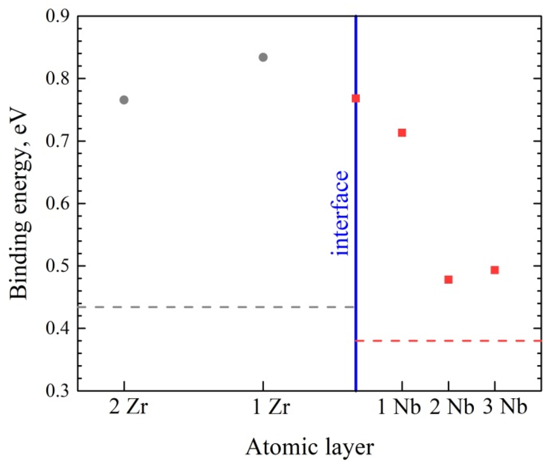
- The average value of hydrogen binding energy decreased with an increase in the distance between the atomic layer and interface slower in the Zr layer than in the Nb layer. Hydrogen diffusion along the interface was more efficient than in the Zr bulk and comparable to diffusion in the Nb bulk.
Author Contributions
Funding
Institutional Review Board Statement
Informed Consent Statement
Data Availability Statement
Acknowledgments
Conflicts of Interest
References
- Zinkle, S.J.; Busby, J.T. Structural Materials for Fission & Fusion Energy. Mater. Today 2009, 12, 12–19. [Google Scholar]
- Odette, G.R.; Hoelzer, D.T. Irradiation-Tolerant Nanostructured Ferritic Alloys: Transforming Helium from a Liability to an Asset. JOM 2010, 62, 84–92. [Google Scholar] [CrossRef]
- Victoria, M.; Baluc, N.; Bailat, C.; Dai, Y.; Luppo, M.I.; Schaublin, R.; Singh, B.N. The Microstructure and Associated Tensile Properties of Irradiated FCC and BCC Metals. J. Nucl. Mater. 2000, 276, 114–122. [Google Scholar] [CrossRef]
- Zinkle, S.J.; Ghoniem, N.M. Operating Temperature Windows for Fusion Reactor Structural Materials. Fusion Eng. Des. 2000, 51, 55–71. [Google Scholar] [CrossRef]
- Stubbins, J.F. Void Swelling and Radiation-Induced Phase Transformation in High Purity Fe-Ni-Cr Alloys. J. Nucl. Mater. 1986, 141, 748–753. [Google Scholar] [CrossRef]
- Ham, B.; Zhang, X. High Strength Mg/Nb Nanolayer Composites. Mater. Sci. Eng. A 2011, 528, 2028–2033. [Google Scholar] [CrossRef]
- Lu, Y.Y.; Kotoka, R.; Ligda, J.P.; Cao, B.B.; Yarmolenko, S.N.; Schuster, B.E.; Wei, Q. The Microstructure and Mechanical Behavior of Mg/Ti Multilayers as a Function of Individual Layer Thickness. Acta Mater. 2014, 63, 216–231. [Google Scholar] [CrossRef]
- Zhang, J.Y.; Lei, S.; Liu, Y.; Niu, J.J.; Chen, Y.; Liu, G.; Zhang, X.; Sun, J. Length Scale-Dependent Deformation Behavior of Nanolayered Cu/Zr Micropillars. Acta Mater. 2012, 60, 1610–1622. [Google Scholar] [CrossRef]
- Bai, X.-M.; Voter, A.F.; Hoagland, R.G.; Nastasi, M.; Uberuaga, B.P. Efficient Annealing of Radiation Damage near Grain Boundaries via Interstitial Emission. Science 2010, 327, 1631–1634. [Google Scholar] [CrossRef]
- Li, N.; Fu, E.G.; Wang, H.; Carter, J.J.; Shao, L.; Maloy, S.A.; Misra, A.; Zhang, X. He Ion Irradiation Damage in Fe/W Nanolayer Films. J. Nucl. Mater. 2009, 389, 233–238. [Google Scholar] [CrossRef]
- Zhuo, M.J.; Fu, E.G.; Yan, L.; Wang, Y.Q.; Zhang, Y.Y.; Dickerson, R.M.; Uberuaga, B.P.; Misra, A.; Nastasi, M.; Jia, Q.X. Interface-Enhanced Defect Absorption between Epitaxial Anatase TiO2 Film and Single Crystal SrTiO3. Scr. Mater. 2011, 65, 807–810. [Google Scholar] [CrossRef]
- Wei, Q.M.; Li, N.; Mara, N.; Nastasi, M.; Misra, A. Suppression of Irradiation Hardening in Nanoscale V/Ag Multilayers. Acta Mater. 2011, 59, 6331–6340. [Google Scholar] [CrossRef]
- Chimi, Y.; Iwase, A.; Ishikawa, N.; Kobiyama, M.; Inami, T.; Okuda, S. Accumulation and Recovery of Defects in Ion-Irradiated Nanocrystalline Gold. J. Nucl. Mater. 2001, 297, 355–357. [Google Scholar] [CrossRef]
- Singh, B.N. Effect of Grain Size on Void Formation during High-Energy Electron Irradiation of Austenitic Stainless Steel. Philos. Mag. J. Theor. Exp. Appl. Phys. 1974, 29, 25–42. [Google Scholar] [CrossRef]
- Nita, N.; Schaeublin, R.; Victoria, M.; Valiev, R.Z. Effects of Irradiation on the Microstructure and Mechanical Properties of Nanostructured Materials. Philos. Mag. 2005, 85, 723–735. [Google Scholar] [CrossRef]
- Shen, T.D.; Feng, S.; Tang, M.; Valdez, J.A.; Wang, Y.; Sickafus, K.E. Enhanced Radiation Tolerance in Nanocrystalline MgGa2O4. Appl. Phys. Lett. 2007, 90, 263115. [Google Scholar] [CrossRef]
- Samaras, M.; Derlet, P.M.; Van Swygenhoven, H.; Victoria, M. Computer Simulation of Displacement Cascades in Nanocrystalline Ni. Phys. Rev. Lett. 2002, 88, 125505. [Google Scholar] [CrossRef] [Green Version]
- Yang, G.H.; Zhao, B.; Gao, Y.; Pan, F. Investigation of Nanoindentation on Co/Mo Multilayers by the Continuous Stiffness Measurement Technique. Surf. Coat. Technol. 2005, 191, 127–133. [Google Scholar] [CrossRef]
- Le Claire, A.D. Diffusion. In Treatise on Solid State Chemistry; Springer: Berlin/Heidelberg, Germany, 1976; pp. 1–59. [Google Scholar]
- Kocks, U.F.; Mecking, H. Physics and Phenomenology of Strain Hardening: The FCC Case. Prog. Mater. Sci. 2003, 48, 171–273. [Google Scholar] [CrossRef]
- Heslop, J.; Petch, N.J. The Ductile-Brittle Transition in the Fracture of α-Iron: II. Philos. Mag. 1958, 3, 1128–1136. [Google Scholar] [CrossRef]
- Valiev, R.Z.; Islamgaliev, R.K.; Alexandrov, I. V Bulk Nanostructured Materials from Severe Plastic Deformation. Prog. Mater. Sci. 2000, 45, 103–189. [Google Scholar] [CrossRef]
- Zhilyaev, A.P.; Langdon, T.G. Using High-Pressure Torsion for Metal Processing: Fundamentals and Applications. Prog. Mater. Sci. 2008, 53, 893–979. [Google Scholar] [CrossRef]
- Valiev, R. Nanostructuring of Metals by Severe Plastic Deformation for Advanced Properties. Nat. Mater. 2004, 3, 511–516. [Google Scholar] [CrossRef] [PubMed]
- Fukai, Y.; Okuma, N. Formation of Superabundant Vacancies in Pd Hydride under High Hydrogen Pressures. Phys. Rev. Lett. 1994, 73, 1640. [Google Scholar] [CrossRef]
- Shirai, Y.; Araki, H.; Mori, T.; Nakamura, W.; Sakaki, K. Positron Annihilation Study of Lattice Defects Induced by Hydrogen Absorption in Some Hydrogen Storage Materials. J. Alloys Compd. 2002, 330, 125–131. [Google Scholar] [CrossRef]
- Mishin, I.P.; Grabovetskaya, G.P.; Stepanova, E.N.; Laptev, R.S.; Teresov, A.D. Hydrogen Effect on the Defect Structure Formation in the Zr—1 WT.% Nb Alloy under Pulsed Electron Beam Irradiation. Russ. Phys. J. 2019, 62, 854–860. [Google Scholar] [CrossRef]
- Kuznetsov, P.V.; Mironov, Y.P.; Tolmachev, A.I.; Bordulev, Y.S.; Laptev, R.S.; Lider, A.M.; Korznikov, A. V Positron Spectroscopy of Defects in Submicrocrystalline Nickel after Low-Temperature Annealing. Phys. Solid State 2015, 57, 219–228. [Google Scholar] [CrossRef]
- Stepanova, E.; Bordulev, Y.; Kudiiarov, V.; Laptev, R.; Lider, A.; Xinming, J. Effect of Hydrogen on the Structural and Phase State and Defect Structure of Titanium Alloy. In AIP Conference Proceedings; AIP Publishing LLC: Malappuram, India, 2016; Volume 1772, p. 30016. [Google Scholar]
- Laptev, R.S.; Lider, A.M.; Bordulev, Y.S.; Kudiiarov, V.N.; Garanin, G.V.; Wang, W.; Kuznetsov, P.V. Investigation of Defects in Hydrogen-Saturated Titanium by Means of Positron Annihilation Techniques. Defect Diffus. Forum 2015, 365, 232–236. [Google Scholar] [CrossRef]
- Č’ižek, J.; Melikhova, O.; Procházka, I. Hydrogen-Induced Defects and Multiplication of Dislocations in Palladium. J. Alloys Compd. 2015, 645, S312–S315. [Google Scholar] [CrossRef]
- Yu, K.Y.; Liu, Y.; Fu, E.G.; Wang, Y.Q.; Myers, M.T.; Wang, H.; Shao, L.; Zhang, X. Comparisons of Radiation Damage in He Ion and Proton Irradiated Immiscible Ag/Ni Nanolayers. J. Nucl. Mater. 2013, 440, 310–318. [Google Scholar] [CrossRef]
- Chen, F.; Tang, X.; Huang, H.; Liu, J.; Li, H.; Qiu, Y.; Chen, D. Surface Damage and Mechanical Properties Degradation of Cr/W Multilayer Films Irradiated by Xe20+. Appl. Surf. Sci. 2015, 357, 1225–1230. [Google Scholar] [CrossRef]
- Fu, E.G.; Carter, J.; Swadener, G.; Misra, A.; Shao, L.; Wang, H.; Zhang, X. Size Dependent Enhancement of Helium Ion Irradiation Tolerance in Sputtered Cu/V Nanolaminates. J. Nucl. Mater. 2009, 385, 629–632. [Google Scholar] [CrossRef]
- Demkowicz, M.J.; Hoagland, R.G.; Hirth, J.P. Interface Structure and Radiation Damage Resistance in Cu-Nb Multilayer Nanocomposites. Phys. Rev. Lett. 2008, 100, 136102. [Google Scholar] [CrossRef] [PubMed]
- Misra, A.; Demkowicz, M.J.; Zhang, X.; Hoagland, R.G. The Radiation Damage Tolerance of Ultra-High Strength Nanolayered Composites. JOM 2007, 59, 62–65. [Google Scholar] [CrossRef]
- Laptev, R.; Lomygin, A.; Krotkevich, D.; Syrtanov, M.; Kashkarov, E.; Bordulev, Y.; Siemek, K.; Kobets, A. Effect of Proton Irradiation on the Defect Evolution of Zr/Nb Nanoscale Multilayers. Metals 2020, 10, 535. [Google Scholar] [CrossRef] [Green Version]
- Ziegler, J.F.; Ziegler, M.D.; Biersack, J.P. SRIM—The Stopping and Range of Ions in Matter (2010). Nucl. Instrum. Methods Phys. Res. Sect. B Beam Interact. Mater. At. 2010, 268, 1818–1823. [Google Scholar] [CrossRef] [Green Version]
- Vehanen, A.; Saarinen, K.; Hautojärvi, P.; Huomo, H. Profiling Multilayer Structures with Monoenergetic Positrons. Phys. Rev. B 1987, 35, 4606. [Google Scholar] [CrossRef]
- The S-Parameter Evaluation. Available online: https://ifj.edu.pl/private/jdryzek/page_r18.html (accessed on 29 April 2022).
- Shulepov, I.; Lomygin, A.; Roman, L.; Kashkarov, E.; Syrtanov, M. Correction of the Distribution Profiles of the Intensities of Elements Considering the Uneven Dispersion of the Glow-Discharge Optical Emission Spectrometer for Multilayer Coatings Analysis. In Proceedings of the 2020 7th International Congress on Energy Fluxes and Radiation Effects (EFRE), Tomsk, Russia, 14–26 September 2020; pp. 1155–1159. [Google Scholar]
- Giannozzi, P.; Andreussi, O.; Brumme, T.; Bunau, O.; Nardelli, M.B.; Calandra, M.; Car, R.; Cavazzoni, C.; Ceresoli, D.; Cococcioni, M.; et al. Advanced Capabilities for Materials Modelling with Quantum ESPRESSO. J. Phys. Condens. Matter 2017, 29, 465901. [Google Scholar] [CrossRef] [Green Version]
- Gonze, X.; Amadon, B.; Antonius, G.; Arnardi, F.; Baguet, L.; Beuken, J.-M.; Bieder, J.; Bottin, F.; Bouchet, J.; Bousquet, E.; et al. The ABINIT Project: Impact, Environment and Recent Developments. Comput. Phys. Commun. 2020, 248, 107042. [Google Scholar] [CrossRef]
- Romero, A.H.; Allan, D.C.; Amadon, B.; Antonius, G.; Applencourt, T.; Baguet, L.; Bieder, J.; Bottin, F.; Bouchet, J.; Bousquet, E.; et al. ABINIT: Overview and Focus on Selected Capabilities. J. Chem. Phys. 2020, 152, 124102. [Google Scholar] [CrossRef]
- Tao, J.; Perdew, J.P.; Tang, H.; Shahi, C. Origin of the Size-Dependence of the Equilibrium van Der Waals Binding between Nanostructures. J. Chem. Phys. 2018, 148, 74110. [Google Scholar] [CrossRef] [PubMed] [Green Version]
- Laptev, R.; Svyatkin, L.; Krotkevich, D.; Stepanova, E.; Pushilina, N.; Lomygin, A.; Ognev, S.; Siemek, K.; Uglov, V. First-Principles Calculations and Experimental Study of H+-Irradiated Zr/Nb Nanoscale Multilayer System. Metals 2021, 11, 627. [Google Scholar] [CrossRef]
- Domain, C.; Besson, R.; Legris, A. Atomic-Scale Ab-Initio Study of the Zr-H System: I. Bulk Properties. Acta Mater. 2002, 50, 3513–3526. [Google Scholar] [CrossRef]
- Svyatkin, L.A.; Koroteev, Y.M.; Chernov, I.P. First Principle Calculations of Diffusion Barriers for Hydrogen in $α$-Zirconium. In Advanced Materials Research; Trans Tech Publications Ltd.: Stafa-Zurich, Switzerland, 2015; Volume 1084, pp. 133–137. [Google Scholar]
- Olsen, R.A.; Kroes, G.J.; Henkelman, G.; Arnaldsson, A.; Jónsson, H. Comparison of Methods for Finding Saddle Points without Knowledge of the Final States. J. Chem. Phys. 2004, 121, 9776–9792. [Google Scholar] [CrossRef]
- Callisti, M.; Karlik, M.; Polcar, T. Competing Mechanisms on the Strength of Ion-Irradiated Zr/Nb Nanoscale Multilayers: Interface Strength versus Radiation Hardening. Scr. Mater. 2018, 152, 31–35. [Google Scholar] [CrossRef] [Green Version]
- Du, J.W.; Chen, L.; Chen, J.; Du, Y. Mechanical Properties, Thermal Stability and Oxidation Resistance of TiN/CrN Multilayer Coatings. Vacuum 2020, 179, 109468. [Google Scholar] [CrossRef]
- Callisti, M.; Polcar, T. Combined Size and Texture-Dependent Deformation and Strengthening Mechanisms in Zr/Nb Nano-Multilayers. Acta Mater. 2017, 124, 247–260. [Google Scholar] [CrossRef] [Green Version]
- Jiménez-Villacorta, F.; Prieto, C. Magnetic Properties and Interaction Mechanisms of Iron-Based Core—Shell Structures Prepared by Sputtering at Low Substrate Temperatures. J. Phys. Condens. Matter 2008, 20, 85216. [Google Scholar] [CrossRef]
- Clemens, B.M.; Gay, J.G. Effect of Layer-Thickness Fluctuations on Superlattice Diffraction. Phys. Rev. B 1987, 35, 9337. [Google Scholar] [CrossRef]
- Wu, S.H.; Cheng, P.M.; Wu, K.; Hou, Z.Q.; Wang, Y.Q.; Liang, X.Q.; Li, J.; Kuang, J.; Zhang, J.Y.; Liu, G.; et al. Effect of He-Irradiation Fluence on the Size-Dependent Hardening and Deformation of Nanostructured Mo/Zr Multilayers. Int. J. Plast. 2018, 111, 36–52. [Google Scholar] [CrossRef]
- Chen, Y.; Liu, Y.; Fu, E.G.; Sun, C.; Yu, K.Y.; Song, M.; Li, J.; Wang, Y.Q.; Wang, H.; Zhang, X. Unusual Size-Dependent Strengthening Mechanisms in Helium Ion-Irradiated Immiscible Coherent Cu/Co Nanolayers. Acta Mater. 2015, 84, 393–404. [Google Scholar] [CrossRef] [Green Version]
- Hu, Y.T.; Gong, H.; Chen, L. Fundamental Effects of W Alloying on Various Properties of NbH Phases. Int. J. Hydrogen Energy 2015, 40, 12745–12749. [Google Scholar] [CrossRef]
- Qin, J.; Wang, Z.; Wang, D.; Wu, Y.; Zhong, Y.; Hu, C.; Zhou, H. Dissolution, Diffusion, and Penetration of H in the Group VB Metals Investigated by First-Principles Method. Int. J. Hydrogen Energy 2019, 44, 29083–29091. [Google Scholar] [CrossRef]


Publisher’s Note: MDPI stays neutral with regard to jurisdictional claims in published maps and institutional affiliations. |
© 2022 by the authors. Licensee MDPI, Basel, Switzerland. This article is an open access article distributed under the terms and conditions of the Creative Commons Attribution (CC BY) license (https://creativecommons.org/licenses/by/4.0/).
Share and Cite
Laptev, R.; Stepanova, E.; Pushilina, N.; Svyatkin, L.; Krotkevich, D.; Lomygin, A.; Ognev, S.; Siemek, K.; Doroshkevich, A.; Uglov, V. Distribution of Hydrogen and Defects in the Zr/Nb Nanoscale Multilayer Coatings after Proton Irradiation. Materials 2022, 15, 3332. https://doi.org/10.3390/ma15093332
Laptev R, Stepanova E, Pushilina N, Svyatkin L, Krotkevich D, Lomygin A, Ognev S, Siemek K, Doroshkevich A, Uglov V. Distribution of Hydrogen and Defects in the Zr/Nb Nanoscale Multilayer Coatings after Proton Irradiation. Materials. 2022; 15(9):3332. https://doi.org/10.3390/ma15093332
Chicago/Turabian StyleLaptev, Roman, Ekaterina Stepanova, Natalia Pushilina, Leonid Svyatkin, Dmitriy Krotkevich, Anton Lomygin, Sergei Ognev, Krzysztof Siemek, Aleksandr Doroshkevich, and Vladimir Uglov. 2022. "Distribution of Hydrogen and Defects in the Zr/Nb Nanoscale Multilayer Coatings after Proton Irradiation" Materials 15, no. 9: 3332. https://doi.org/10.3390/ma15093332
APA StyleLaptev, R., Stepanova, E., Pushilina, N., Svyatkin, L., Krotkevich, D., Lomygin, A., Ognev, S., Siemek, K., Doroshkevich, A., & Uglov, V. (2022). Distribution of Hydrogen and Defects in the Zr/Nb Nanoscale Multilayer Coatings after Proton Irradiation. Materials, 15(9), 3332. https://doi.org/10.3390/ma15093332