Article

Numerical Simulation of 30% Efficient Lead-Free Perovskite CsSnGeI3-Based Solar Cells

College of Engineering and Technology, American University of the Middle East, Kuwait
Materials 2022, 15(9), 3229; https://doi.org/10.3390/ma15093229
Submission received: 17 March 2022 / Revised: 26 April 2022 / Accepted: 27 April 2022 / Published: 29 April 2022
(This article belongs to the Special Issue Metal Oxides for Photovoltaic and Photocatalytic Applications)

Abstract

:
A cesium tin–germanium triiodide (CsSnGeI3) perovskite-based solar cell (PSC) has been reported to achieve a high-power-conversion efficiency (PCE > 7%) and extreme air stability. A thorough understanding of the role of the interfaces in the perovskite solar cell, along with the optimization of different parameters, is still required for further improvement in PCE. In this study, lead-free CsSnGeI3 PSC has been quantitatively analyzed using a solar cell capacitance simulator (SCAPS–1D). Five electron transport layers (ETL) were comparatively studied, while keeping other layers fixed. The use of SnO2 as an ETL, which has the best band alignment with the perovskite layer, can increase the power conversion efficiency (PCE) of PSC by up to 30%. The defect density and thickness of the absorber layer has been thoroughly investigated. Results show that the device efficiency is highly governed by the defect density of the absorber layer. All the PSCs with a different ETL exhibit PCE exceeding 20% when the defect density of the absorber layer is in the range of 1014 cm−3–1016 cm−3, and degrade dramatically at higher values. With the optimized structure, the simulation found the highest PCE of CsSnGeI3-based PSCs to be 30.98%, with an open circuit voltage (Voc) of 1.22 V, short-circuit current density (Jsc) of 28.18 mA·cm−2, and fill factor (FF) of 89.52%. Our unprecedented results clearly demonstrate that CsSnGeI3-based PSC is an excellent candidate to become the most efficient single-junction solar cell technology soon.

1. Introduction

Energy consumption is expected to increase, with the bulk of the demand coming from developing countries. Conventional fuel remains the greatest contributor to electricity generation worldwide. Producing energy from these resources takes a severe toll on our environment. Solar energy is one of the most abundant energy resources on Earth, as it is sustainable and inexhaustible. Solar cells are regarded as clean and sustainable sources of energy [1,2]. Coupled with an efficiency rating of greater than 15 % , they are a great energy resource [3,4]. To date, conventional silicon (C–Si) solar cells enjoy a market share exceeding 90 % of the overall photovoltaic market [5], due to silicon’s high stability and power conversion efficiency ( P C E ). Theoretically, the room-temperature power conversion efficiency of a single junction C–Si solar cell is limited to 32.33 % [6]. Kaneka Corporation achieved a real-world solar cell with 26.7 % conversion efficiency [7,8]. However, there are several drawbacks, namely high cost, difficult preparation conditions, serious environmental pollution [9], and the indirect nature of its electronic band gap, making it a relatively weak absorber of long wavelength sunlight [10].
A decade ago, lead halide Perovskite solar cells (PSCs) emerged as a breakthrough photovoltaic (PV) technology. These cells have acquired significant interest in research and industrial communities due to their high-power-conversion efficiency exceeding 25 % [11,12,13], straightforward fabrication process, and relatively low cost [14,15]. The state-of-the-art certified P C E of PSC in single junction architectures exceeded 25% in less than 10 years [16,17], owing to its tunable direct bandgap, high absorption coefficient, low exciton binding energy, and high carrier mobility [18,19,20,21]. Although the perovskite community has put great efforts into addressing the peculiar physics and chemistry of these materials, and has achieved remarkable results, the toxicity of lead associated with the lifecycle of these PSCs is a major concern, hindering their commercialization and future large-scale applications. To conquer this issue, scientists have devoted huge efforts to substitute lead with non-toxic metals such as tin, bismuth, and germanium [22,23,24,25].
Tin-based halide perovskites, such as CsSnI3, CH3NH3SnI3 (MASnI3), and HC(NH2)2SnI3 (FASnI3), have been investigated. The latter two perovskites have intrinsically low stability [26,27]. The all-inorganic lead-free CsSnI3 perovskite could be a promising alternative to Pb-based light harvesting materials, due to its improved photoelectric characteristics such as a high absorption coefficient, small exciton binding energy, high carrier mobility, etc., and is currently the strongest candidate [28,29,30,31]. Recently, several studies showed that the substitution of the organic cation by cesium (Cs) in the perovskite structure could significantly enhance its thermal stability and outdoor/ambient device performance [32,33]. Among all lead-free all-inorganic PSCs, CsSnI3 recorded the highest P C E of 10.1 % [34,35]. Min Chen et al. [36] proposed a perovskite absorber material CsSnGeI3 that shows superior performance and exceptional air stability over its pure counterparts CsSnI3 and CsGeI3. The CsSnGeI3-based device shows a P C E of 7%.
This study aims to suggest possible optimization routes for efficiency improvements of the CsSnGeI3 perovskite solar cell, by analyzing various device parameters using a solar cell capacitance simulator (SCAPS-1D) [37]. Different types of simulation software exist, to study the perovskite solar cell performance via computational investigation, such as SILVACO ATLAS, AMPS, COMSOL, and SCAPS [38,39]. Among them, SCAPS presents unique advantages, such as the ability to simulate up to seven different layers with non-routine measurements (C-V, C-f). It can calculate many parameters such as spectral response, energy bands, ac characteristics, J−V curve, and defect density, by just solving three basic semiconductor equations. It is user friendly and may be executed in both dark and light atmospheres [40,41,42]. Several studies confirm the good agreement of the simulation results with the experimental data, indicating the reliability of SCPAS software [43,44].
This work focuses on engineering the interface ETL/perovskite absorber layer. Optimizing the interfaces in the PCSs is essential for enhancing the photovoltaic performance. In this study, different materials were investigated as ETL, mainly TiO2 and SnO2. TiO2 is the most common ETL for the fabrication of PSC [41]. On the other hand, SnO2 has high electron mobility and keeps better band alignment with the CsSnGeI3 absorber layer, which is supportive for electron extraction [45,46]. Cuprous oxide Cu2O was used as the hole transport layer (HTL) due to its low cost, and it is widely used in solar energy materials, as a promising inorganic HTL for PSC applications [47]. The impact of the defect density and the thickness of the absorber layer on the overall performance of the proposed device was studied. For the first time, we show that an optimum CsSnGeI3 device can have a simulated power conversion efficiency P C E of 30 % .

2. Materials and Methods

In this numerical modeling, a comprehensive study has been performed on CsSnGeI3, as the light harvesting material using SCAPS, which is 1D solar cell simulation software [47]. The software is specially designed to simulate multilayer solar cells, up to seven layers. SCAPS permits the calculation and observation of many electrical characteristics and parameters including current-density ( J V ) curve, hetero-junction energy band structure, quantum efficiency ( Q E ), open circuit voltage V o c , short circuit J s c , current density, power conversion efficiency ( P C E ) , fill factor ( F F ) , etc. The algorithm of SCPAS software is developed to solve the Poisson equation (Equation (1)) and the continuity equation of both charge carriers, electron (Equation (2)), and hole (Equation (3)).
d d x ε x d ψ d x = q p x n x + N D + x N A x + p t x n t x
d p n d t = G p p n p n 0 τ p + p n μ p d ξ d x + μ p ξ d p n d x + D p d 2 p n d x 2
d n p d t = G n n p n p 0 τ n + n p μ n d ξ d x + μ n ξ d n p d x + D n d 2 n p d x 2
The device simulation is carried out in the n i p configuration of FTO/ETL/CsSnGeI3/Cu2O/Au, which is represented in Figure 1b. It was performed at 300   K under a standard illumination of 1000   W / m 2 and an air mass of AM 1.5G. The absorber layer is sandwiched between the HTL and ETL layers. Fluorine-doped tin oxide (FTO) is used as a front contact and gold (Au) as back metal contact. HTM Cu2O is used for every structure, while five different ETLs are alternately used, and their performances are compared. The ETL includes: SnO2, ZnO, IGZO, CdS, and TiO2. Figure 1a shows the energy level diagram of the corresponding materials utilized in the device structure.
Table 1, Table 2 and Table 3 show the list of values extracted from theories, experiments, and the literature [48,49,50,51,52,53,54,55,56,57]. The parameters have been considered, while forming a base configuration to start with the simulation process. Different properties, such as the thickness and defect density of the absorber layer, have been varied to obtain an optimized result and to study their impacts on the device performance. Initially, the thickness of FTO 400   nm , ETL 50   nm , and Cu2O 350   nm were optimized for high P C E , as mentioned in Table 1.

3. Results and Discussions

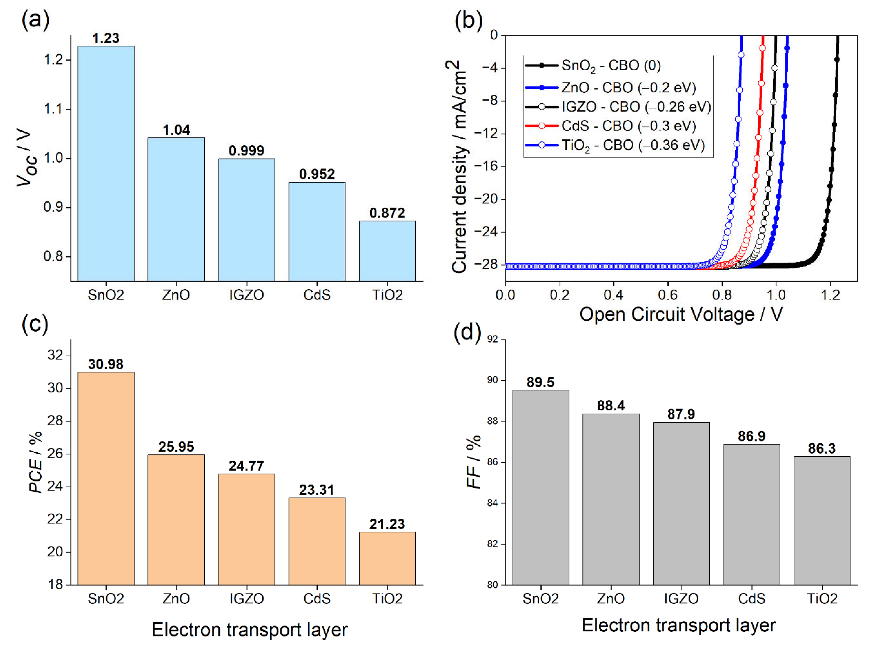
3.1. Effect of ETLs on Solar Cell Performance

The n i p PSC structures for three different ETL are analyzed for the same absorber (CsSnGeI3) layer thickness, 1.5   μ m , and the same absorber bulk defect densities, 1 × 10 15   cm 3 . It should be mentioned that these values are selected and fixed after optimizing the device performance. The thickness and the defect concentration of the perovskite layer were investigated and varied, until the optimal performance of the solar cell is found. The J V characteristics for the five structures are shown in Figure 2a, while the open circuit voltage ( V o c ), performance cell efficiency ( P C E ) , and fill factor ( F F ) are plotted, respectively, in Figure 2b–d. Figure 2b reveals that the five simulated cells exhibit the same current level of 28   mA · cm 2 .
Surprisingly, all ETLs had superior performance over TiO2, the most commonly used ETL in perovskite studies due to its mesoscopic structure. It is observed that the PSC with SnO2 acquired the highest P C E   of 30.9 % and V o c of 1.22   V . The most credible reason of this behavior is the excellent band alignment with the CsSnGeI3 layer shown in Figure 1a, where there is no conduction band offset (CBO) ( Δ E c = 0 ) at the SnO2/CsSnGeI3 interface. In fact, CBO is the energy difference Δ E c between the CB level of ETL and that of the perovskite. When the CB level of ETL is lower than that of the perovskite, Δ E c will be negative and an energy cliff will be formed at the ETL/perovskite interface. An energy cliff structure does not hinder the photo-generated electron flow, but it may cause the interfacial recombination to occupy the main position of recombination of the PSC device [58,59]. When the energy cliff is formed, there is no potential barrier for electrons at the ETL/perovskite interface. The energy barrier that the electron transport must overcome from the conduction band of the ETL to the interface ETL/perovskite is Δ E c + q V D , here q is the charge of the carrier and V D is the built-in potential. Since Δ E c is negative for all devices, except the one with SnO2 ETL, the electrons in the ETL layer can easily cross the barrier to attain the interface. The cliff formation can improve the accumulation near to ETL/perovskite, which in turn enhances the recombination in this area by back-transfer to the interface of heterojunction.
Under open-circuit conditions, the interfacial recombination mainly occurs through the pathways of back-transfer recombination, where the electrons that have been injected into the FTO electrode, and the free holes in the absorber recombine through the deep level defect at the ETL/absorber interface, which then result in a serious V o c deficit. Then, the P C E drops, which has been confirmed by our results plotted in Figure 2a,c. They exhibit that the V o c as well as the P C E dramatically decrease with the increase in the absolute value of Δ E c . It was observed in Figure 2d that F F is improved with devices having a larger V o c . The solar cell with the benchmark material TiO2 ETL yields the lowest P C E of 21.23 % , Voc of 0.872   V , and FF of 86.3 % , owing this to the largest CBO among all the tested materials ( Δ E c = 0.36   eV ), comparable to the best performance obtained in recent studies on similar perovskite [60].
Finally, it can be concluded that the band alignment plays one of the key roles for having higher P C E ,   V o c , and F F . Thus, SnO2 is finally selected as the optimal ETL material for the proposed lead-free PSC.

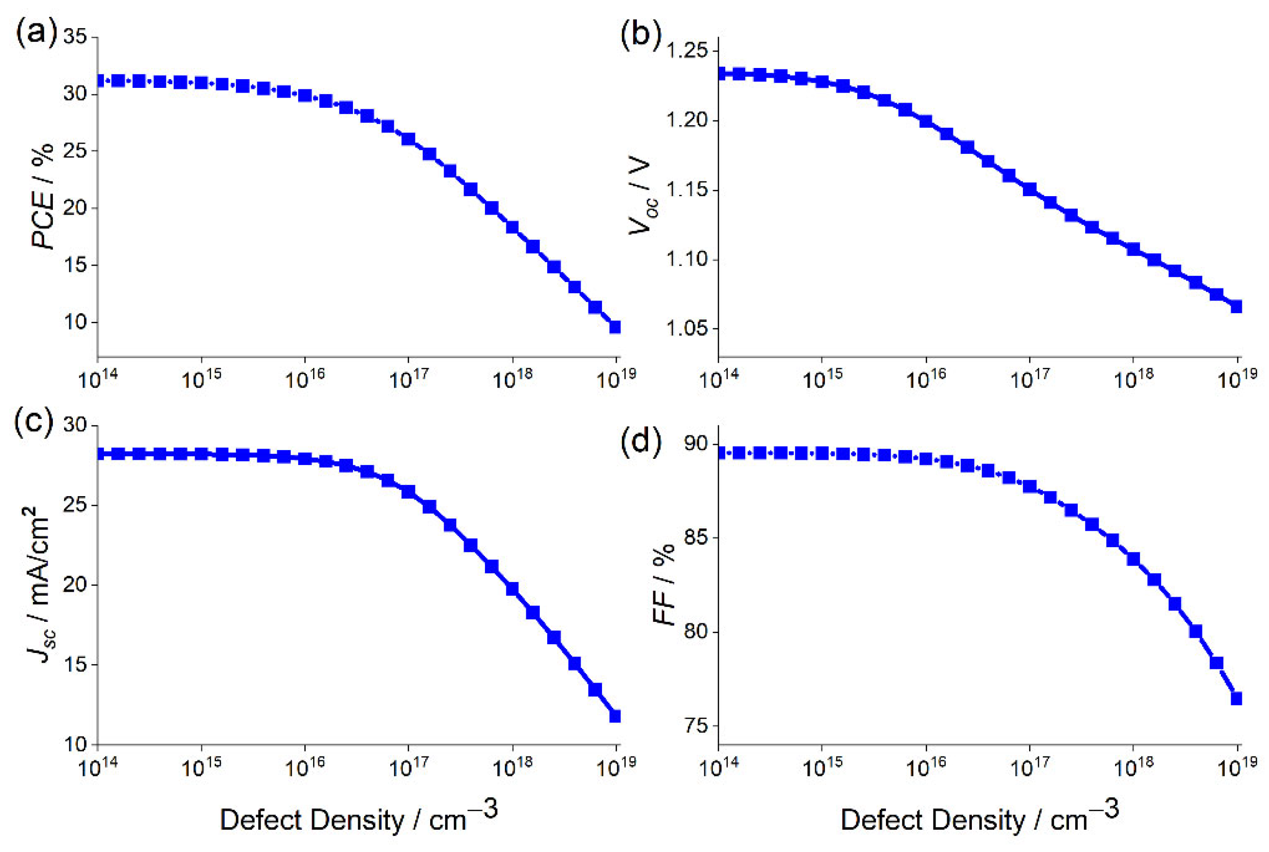
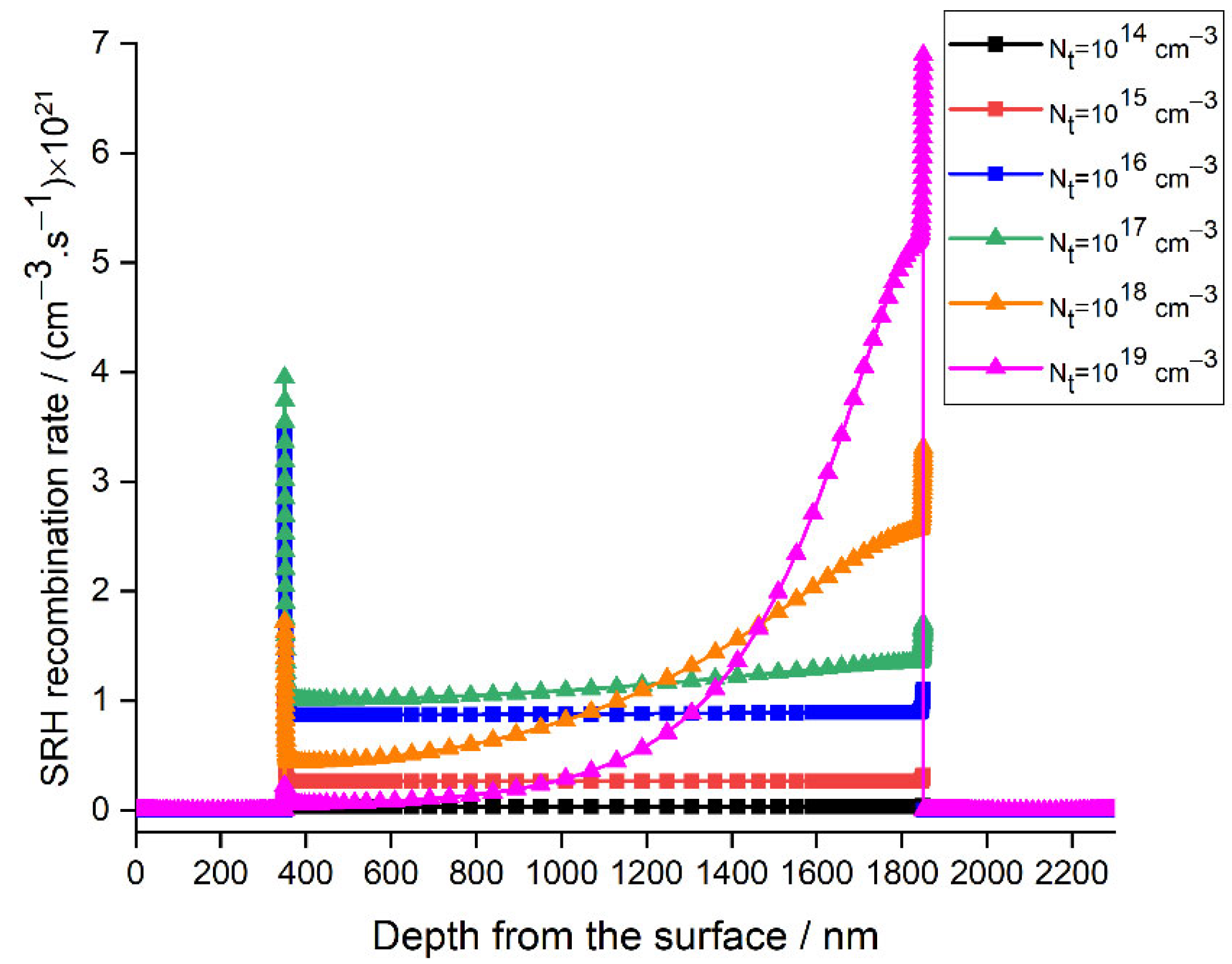
3.2. Effect of Absorber Layer Defects Density N t

Although the interface engineering and the control at the ETL/perovskite interface is crucial for achieving a high-efficiency solar cell device, the morphology and quality of the light absorber film have been recently recognized as a major factor for determining PSC performance [61], given that the photoelectrons are mainly generated in this layer. Thus, to further enhance the PSC performance with SnO2 ETL and to determine the influence of absorber defect density on cell performance, the defect density of the perovskite layer has been considered. The defect density values simulated in this study range from 10 14 cm 3 to 10 19   cm 3 , based on values from previous studies on lead [62,63]. As shown in Figure 3a–d, when the defect density is below N t = 10 16   cm 3 , the photovoltaic response of the cell remains almost unchanged, except V o c , which starts to decrease. The PSC performance properties start to deteriorate when the defect density exceeds 10 16   cm 3 , until reaching their lowest performance values of V o c = 1.06   V , J s c = 11.79   mA · cm 2 , P C E = 9.61 % , and F F = 76.46 % .
The perovskite defect density effect can be explained by the Shockley–Read–Hall (SRH) recombination model [64,65]. In this work, to clearly understand the defect density effect of the absorber on the performance of the device, the variation of the SRH recombination rate with depth from the surface for different values of defect density was studied and depicted in Figure 4. It is detected that the recombination rate increases with the increase in the defect density. Consequently, V o c and P C E decrease, as shown in Figure 3a,b. It can be observed that the recombination rate not only increases in the absorber layer between 350   nm and 1850   nm but also at the perovskite/ETL interface, reaching a maximum of 7 × 10 21   cm 3 · s 1 .
According to the SRH model, the recombination rate can be expressed by:
R S R H = τ n , p 1 n · p n i 2 n + p + 2 n i c o h E t E i K T
where, τ n , p , n , p , n i , E i , and E t represent the lifetime of charge carriers, electron density, hole density, intrinsic density, intrinsic energy level, and energy level of the trap defects, respectively.
The lifetime of charge carriers ( τ n , p ) , the diffusion coefficient D , and the diffusion length of charge carrier ( L D ) are represented in the following equations:
τ n , p = 1 σ n , p v t h N t
L D = D τ
D = μ · K B T q
where μ is the mobility of charge carriers, T is the temperature in Kelvin, K B is the Boltzmann constant, and q the magnitude of the charge.
It can be deduced from Equations (4)–(7) that as the defect density in the perovskite layer increases, the carrier lifetime decreases, while the charge recombination will increase, as confirmed in Figure 4, leading to a drop in V o c and J s c . Moreover, when the doping density is comparable or lower than that of the defect density in the absorber, the device becomes semi-insulating and the desired p-n junction will not be formed [66], resulting in inferior cell performance. This scenario was confirmed by the current study, wherein the doping density for CsSnGeI3 is 10 17   cm 3 , and the performance of the device starts to worsen when the defect density exceeds 10 16   cm 3 .
It can be observed from Equation (7) that the diffusion coefficient is proportional to the mobility of charge carrier, the electron mobility ( 974   cm 2 / V · s ), and hole mobility ( 213   cm 2 / V · s ), being larger for CsSnGeI3. Due to the large value of mobility, the diffusion length is high, and that is why our simulated PSC shows a high efficiency of 30.98 % with N t = 10 15   cm 3 . Thus, to achieve optimum PSC performance, the defect density in the absorber layer has to be significantly reduced. Experimental studies have proven that the fabrication of the tin-based perovskite device, with defect density as low as N t = 10 15   cm 3 , is completely feasible [67], so we set this defect density as an optimized value. By fixing N t = 10 15 cm 3 , the cell performance reaches its maximum performance, attaining a J s c of 28.19   mA · cm 2 , P C E of 30.98 % , F F of 89.52 % , and V o c of 1.22   V . Further decreasing the defect density from N t = 10 15   cm 3 to N t = 10 14   cm 3 has a negligible effect. The obtained performance is found to be largely better than the previously published results for lead-free perovskite solar cells [60].

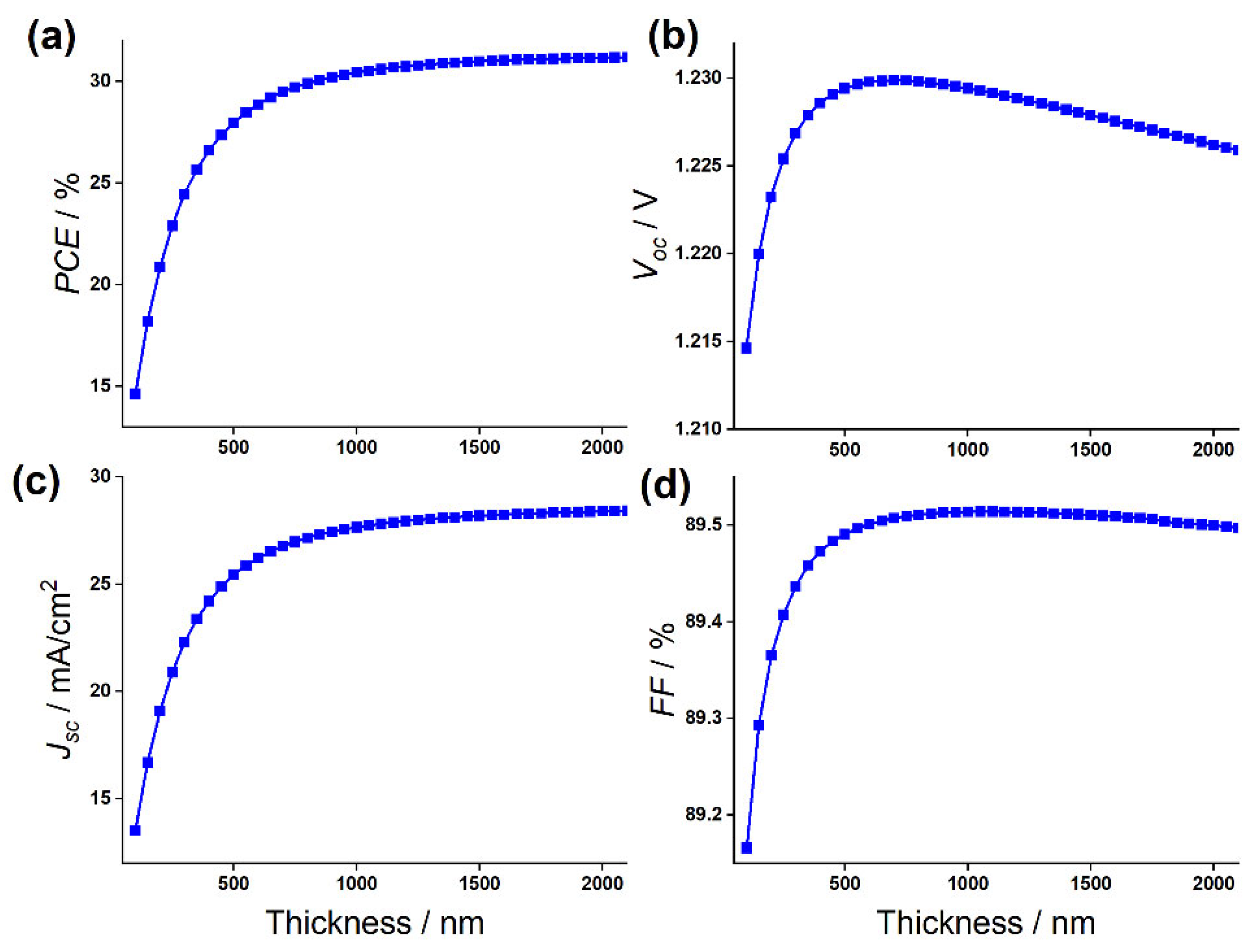
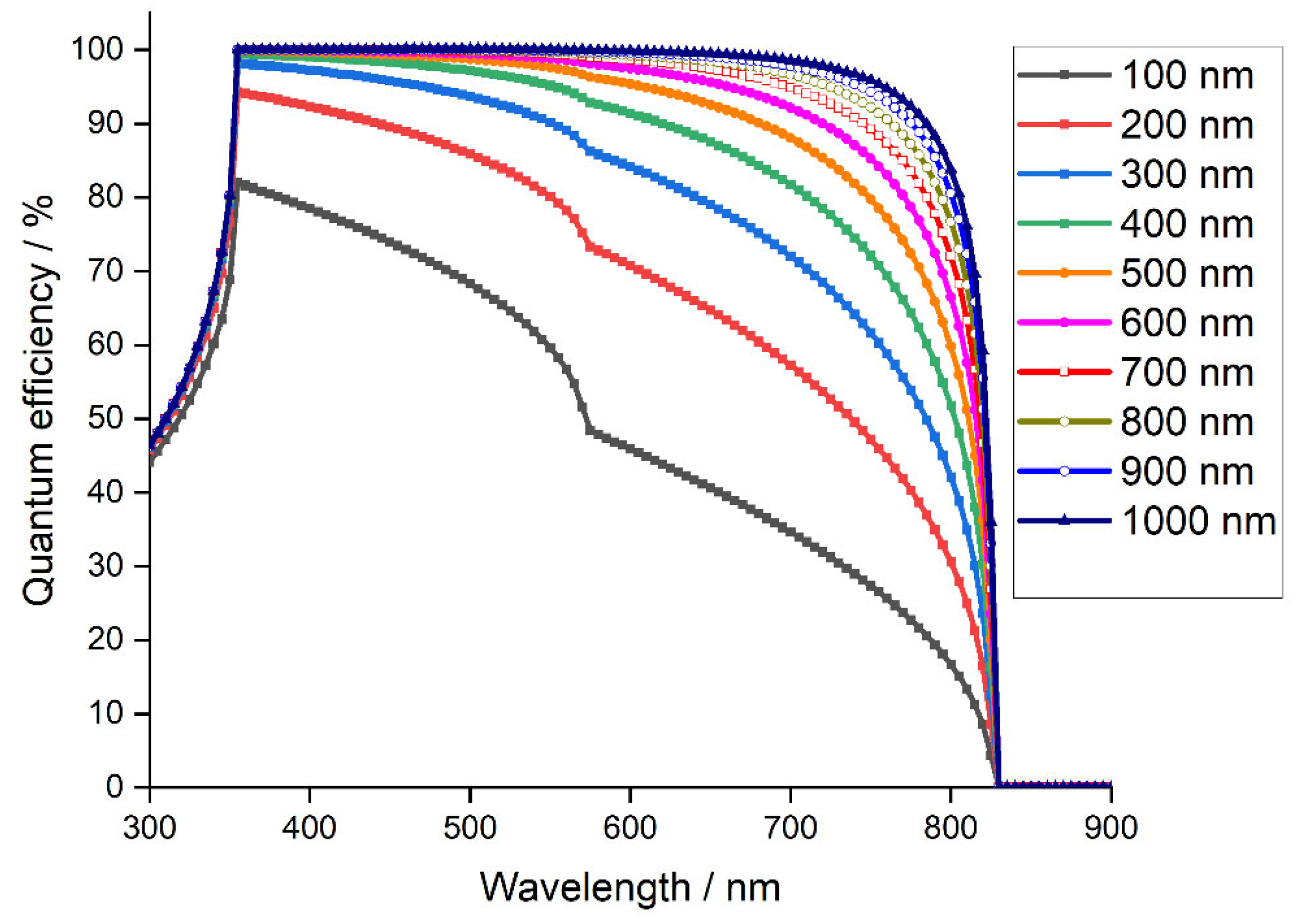
3.3. Influence of the Absorber Layer Thickness

The thickness of the light-absorbing layer plays a crucial role in optimizing the solar cell performance. It should be chosen as high to maximize the current density, but not too much, as it minimizes the reverse saturation current. The influence of the absorber layer thickness on the device photovoltaic outputs has been studied, by varying it from 0.1   μ m to 2   μ m while maintaining all the other parameters as given in Table 1. Figure 5a–d depicts the PSC performance statistics, including V o c , J s c , P C E , and F F . It can be observed that the effect of absorber layer thickness is minimal. A F F of 89.16 % and 89.50 % are obtained at an absorber layer thickness of 0.1   μ m and 0.6   μ m , respectively, then it saturates. The value of V o c is obtained to be 1.214   V at 0.1   μ m and increases up to a maximum of 1.230   V at 0.6   μ m , then it decreases to 1.225   V at 0.6   μ m . The decreases in V o c with thickness is attributed to the increase in the dark saturation current, which increases the recombination of the charge carrier. This dependency of the dark saturation current J 0 , V o c , and J s c , is given by [68]:
V o c = K B T q L n J s c J 0 + 1
It is seen in Figure 5c that J s c increases linearly, up to an absorber thickness of 1   μ m , then it almost saturates with an increasing absorber thickness. The J s c of 13.51   mA · cm 2 and 28.45   mA · cm 2 are estimated for a thickness of 0.1 and 2   μ m , respectively. The great enhancement of J s c , with an increase in the absorber thickness, is attributed to the generation of more electron-hole pairs in the perovskite, leading to an efficiency enhancement. The trend of P C E as a function of CsSnGeI3 was strongly correlated with the trend of J s c , and P C E s of 14.63 % and 31 % are estimated for a thickness of 0.1 and 2   μ m , respectively.
Figure 6 depicts quantum efficiency vs. wavelength for various absorber thicknesses ranging from 0.1   μ m . to 1   μ m . Quantum efficiency indicates to what extent a solar cell can collect carriers from incident photons of a given energy. It can be observed that the decrease in absorber thickness leads to reduced photon absorption at a longer wavelength. This is due to fewer photogenerated electron-hole pairs inside the absorber layer. In addition, at wavelengths larger than 830   nm , quantum efficiency falls to zero as light is not absorbed below the bandgaps, at longer, low energy wavelengths. A loss of quantum efficiency can be observed for wavelengths below 350 nm for all simulated solar cells. This is because the light is mainly absorbed by the FTO substrate and SnO2 layer.
The larger QE is reached with an absorber thickness of 1   μ m . Ultimately, the best performing device has a perovskite layer 1.5   μ m thick with J s c of 28.19   mA · cm 2 , P C E of 30.98 % , F F of 89.52 % , and V o c of 1.22   V .

4. Conclusions

In this work, a novel lead-free CsSnGeI3-based perovskite solar cell has been thoroughly investigated. A normal n-i-p planar structure of FTO/ETL/CsSnGeI3/Cu2O/Au is numerically simulated and analyzed using SCAPS-1D simulation software. The impact of various ETL on the device performance was studied to get the highest possible efficiency. It has been demonstrated that a PSC with SnO2 ETL has, by far, the best performance, owing to its excellent band alignment with the perovskite layer. Furthermore, the photovoltaic performance of the cell has been optimized by tuning two major factors: CsSnGeI3 defect density and absorber layer thickness. Our study explained the significant effect of these two factors on the electrical parameters of the PSC. The results revealed that the optimal light absorber thickness and the optimal absorber defect density were 1.5   μ m and 10 15   cm 3 , respectively. Reducing the absorber defect density significantly enhances the P C E to reach an unprecedented result of almost 31 % . Thus, future research should focus on refining the device fabrication techniques. Our novel results could provide a viable path to fabricate cost-effective, highly efficient, and stable CsSnGeI3-based perovskite solar cells.

Funding

This research received no external funding.

Institutional Review Board Statement

Not applicable.

Informed Consent Statement

Not applicable.

Data Availability Statement

Not applicable.

Acknowledgments

The author would like to acknowledge Marc Burgelman (University of Gent) for providing the simulation software SCAPS. The author thanks Jack Arayro ([email protected]) for language editing.

Conflicts of Interest

The author declares no conflict of interest.

References

  1. Grätzel, M. The light and shade of perovskite solar cells. Nat. Mater. 2014, 13, 838–842. [Google Scholar] [CrossRef] [PubMed]
  2. Bhattacharya, S.; John, S. Beyond 30% Conversion Efficiency in Silicon Solar Cells: A Numerical Demonstration. Sci. Rep. 2019, 9, 12482. [Google Scholar] [CrossRef] [PubMed]
  3. Tawalbeh, M.; Al-Othman, A.; Kafiah, F.; Abdelsalam, E.; Almomani, F.; Alkasrawi, M. Environmental impacts of solar photovoltaic systems: A critical review of recent progress and future outlook. Sci. Total Environ. 2021, 759, 143528. [Google Scholar] [CrossRef] [PubMed]
  4. Green, M.A. Tracking solar cell conversion efficiency. Nat. Rev. Phys. 2020, 2, 172–173. [Google Scholar] [CrossRef]
  5. Kour, R.; Arya, S.; Verma, S.; Gupta, J.; Bandhoria, P.; Bharti, V.; Datt, R.; Gupta, V. Potential Substitutes for Replacement of Lead in Perovskite Solar Cells: A Review. Glob. Chall. 2019, 3, 1900050. [Google Scholar] [CrossRef] [PubMed] [Green Version]
  6. Shockley, W.; Queisser, H.J. Detailed balance limit of efficiency of p-n junction solar cells. J. Appl. Phys. 1961, 32, 510. [Google Scholar] [CrossRef]
  7. Yoshikawa, K.; Kawasaki, H.; Yoshida, W.; Irie, T.; Konishi, K.; Nakano, K.; Uto, T.; Adachi, D.; Kanematsu, M.; Uzu, H.; et al. Silicon Heterojunction solar cell with interdigitated back contacts for a photoconversion efficiency over 26%. Nat. Energy 2017, 2, 17032. [Google Scholar] [CrossRef]
  8. Levi, D.H.; Green, M.A.; Hishikawa, Y.; Dunlop, E.D.; Hohl-Ebinger, J.; Ho-Baillie, A.W. Solar cell efficiency tables (version 51). Prog. Photovolt. Res. Appl. 2018, 26, 3. [Google Scholar]
  9. Parida, B.; Iniyan, S.; Goic, R. A review of solar photovoltaic technologies. Sustain. Energy Rev. 2011, 15, 1625. [Google Scholar] [CrossRef]
  10. Saive, R. Light trapping in thin silicon solar cells: A review on fundamentals and technologies. Prog. Photovolt. Res. Appl. 2021, 29, 1125–1137. [Google Scholar] [CrossRef]
  11. Huang, H.H.; Shih, Y.C.; Wang, L.; Lin, K.F. Boosting the ultra-stable unencapsulated perovskite solar cells by using montmorillonite/ CH3NH3PbI3 nanocomposite as photoactive layer. Energy Environ. Sci. 2019, 12, 1265–1273. [Google Scholar] [CrossRef]
  12. Yang, W.S.; Park, B.-W.; Jung, E.H.; Jeon, N.J.; Kim, Y.C.; Lee, D.U.; Shin, S.S.; Seo, J.; Kim, E.K.; Noh, J.H.; et al. Iodide management in formamidinium-lead-halide-based perovskite layers for efficient solar cells. Science 2017, 356, 1376–1379. [Google Scholar] [CrossRef] [PubMed] [Green Version]
  13. Shih, Y.-C.; Lan, Y.-B.; Li, C.-S.; Hsieh, H.-C.; Wang, L.; Wu, C.-I.; Lin, K.-F. Amino-acid-induced preferential orientation of perovskite crystals for enhancing interfacial charge transfer and photovoltaic performance. Small 2017, 13, 1604305–1604314. [Google Scholar] [CrossRef] [PubMed]
  14. Eperon, G.E.; Burlakov, V.M.; Docampo, P.; Goriely, A.; Snaith, H.J. Morphological Control for High Performance, Solution-Processed Planar Heterojunction Perovskite Solar Cells. Adv. Funct. Mater. 2014, 24, 151–157. [Google Scholar] [CrossRef]
  15. Liu, M.; Johnston, M.B.; Snaith, H.J. Efficient planar heterojunction perovskite solar cells by vapour deposition. Nat. Cell Biol. 2013, 501, 395–398. [Google Scholar] [CrossRef]
  16. Kim, H.S.; Im, S.H.; Park, N.G. Organolead halide perovskite: New horizons in solar cell research. J. Phys. Chem. C 2014, 118, 5615–5625. [Google Scholar] [CrossRef]
  17. Gao, F.; Li, C.; Qin, L.; Zhu, L.; Huang, X.; Liu, H.; Liang, L.; Hou, Y.; Lou, Z.; Hu, Y.; et al. Enhanced performance of tin halide perovskite solar cell by addition of lead thiocyanate. RSC Adv. 2018, 8, 14025–14030. [Google Scholar] [CrossRef] [Green Version]
  18. Wang, X.; Zhang, T.; Lou, Y.; Zhao, Y. All-inorganic lead-free perovskites for optoelectronic applications. Mater. Chem. Front. 2019, 3, 365. [Google Scholar] [CrossRef]
  19. Miyata, A.; Mitioglu, A.; Plochocka, P.; Portugall, O.; Wang, J.T.-W.; Stranks, S.D.; Snaith, H.; Nicholas, R. Direct measurement of the exciton binding energy and effective masses for charge carriers in organic–inorganic tri-halide perovskites. Nat. Phys. 2015, 11, 582–587. [Google Scholar] [CrossRef] [Green Version]
  20. Huang, J.; Yuan, Y.; Shao, Y.; Yan, Y. Understanding the physical properties of hybrid perovskites for photovoltaic applications. Nat. Rev. Mater. 2017, 2, 17042. [Google Scholar] [CrossRef]
  21. Jeon, N.J.; Na, H.; Jung, E.H.; Yang, T.-Y.; Lee, Y.G.; Kim, G.; Shin, H.-W.; Seok, S.I.; Lee, J.; Seo, J. A fluorene-terminated hole-transporting material for highly efficient and stable perovskite solar cells. Nat. Energy 2018, 3, 682–689. [Google Scholar] [CrossRef]
  22. Hao, F.; Stoumpos, C.C.; Chang, R.P.H.; Kanatzidis, M.G. Anomalous Band Gap Behavior in Mixed Sn and Pb Perovskites Enables Broadening of Absorption Spectrum in Solar Cells. J. Am. Chem. Soc. 2014, 136, 8094. [Google Scholar] [CrossRef] [PubMed]
  23. Chen, J.; Zhou, S.; Jin, S.; Li, H.; Zhai, T. Crystal organometal halide perovskites with promising optoelectronic applications. J. Mater. Chem. C 2016, 4, 11. [Google Scholar] [CrossRef]
  24. Shen, Q.; Ogomi, Y.; Chang, J.; Toyoda, T.; Fujiwara, K.; Yoshino, K.; Sato, K.; Yamazaki, K.; Akimoto, M.; Kuga, Y.; et al. Optical absorption, charge separation and recombination dynamics in Sn/Pb cocktail perovskite solar cells and their relationships to photovoltaic performances. J. Mater. Chem. A 2015, 3, 9308. [Google Scholar] [CrossRef]
  25. Wang, Y.; Muryobayashi, T.; Nakada, K.; Li, Z.; Yamada, A. Correlation between carrier recombination and valence band offset effect of graded Cu(In,Ga)Se2 solar cells. Sol. Energy Mater. Sol. Cells 2019, 201, 110070. [Google Scholar] [CrossRef]
  26. Dang, Y.; Zhou, Y.; Liu, X.; Ju, D.; Xia, S.; Xia, H.; Tao, X. Formation of hybrid perovskite tin iodide single crystals by topseeded solution growth. Angew. Chem. Int. Ed. 2016, 55, 3447–3450. [Google Scholar] [CrossRef]
  27. Zhou, Y.; Zhou, Z.; Chen, M.; Zong, Y.; Huang, J.; Pang, S.; Padture, N.P. Doping and alloying for improved perovskite solar cells. J. Mater. Chem. A 2016, 4, 17623–17635. [Google Scholar] [CrossRef]
  28. Yu, C.; Chen, Z.; Wang, J.J.; Pfenninger, W.; Vockic, N.; Kenney, J.T.; Shum, K. Temperature dependence of the band gap of perovskite semiconductor compound CsSnI3. J. Appl. Phys. 2011, 110, 063526. [Google Scholar] [CrossRef] [Green Version]
  29. Chung, I.; Lee, B.; He, J.; Chang, R.P.H.; Kanatzidis, M.G. All-solid-state dye-sensitized solar cells with high efficiency. Nature 2012, 485, 486–489. [Google Scholar] [CrossRef]
  30. Chen, Z.; Yu, C.; Shum, K.; Wang, J.J.; Pfenninger, W.; Vockic, N.; Midgley, J.; Kenney, J.T. Photoluminescence study of polycrystalline CsSnI3 thin films: Determination of exciton binding energy. J. Lumin. 2012, 132, 345–349. [Google Scholar] [CrossRef]
  31. Xie, F.; Zhou, S.; Zhao, N.; Hui, H. Native defect-induced hysteresis behavior in organolead iodide perovskite solar cells. Adv. Func. Mater. 2016, 26, 1411–1419. [Google Scholar]
  32. Wang, N.; Zhou, Y.; Ju, M.G.; Garces, H.F.; Ding, T.; Pang, S.; Zeng, X.C.; Padture, N.P.; Sun, X.W. Heterojunction-depleted lead-free perovskite solar cells with coarse-grained B-ϒ-CsSnI3 thin films. Adv. Energy Mater. 2016, 6, 1670137. [Google Scholar]
  33. Marshall, K.P.; Walker, M.; Walton, R.I.; Hatton, R.A. Enhanced stability and efficiency in hole-transport-layer-free CsSnI3 perovskite photovoltaics. Nat. Energy 2016, 1, 16178. [Google Scholar] [CrossRef] [Green Version]
  34. Li, B.; Di, H.; Chang, B.; Yin, R.; Fu, L.; Zhang, Y.; Yin, L. Efficient passivation strategy on Sn related defects for high performance all-inorganic CsSnI3 perovskite solar cells. Adv. Funct. Mater. 2021, 31, 2007447. [Google Scholar] [CrossRef]
  35. Ye, T.; Wang, X.; Wang, K.; Ma, S.; Yang, D.; Hou, Y.; Yoon, J.; Wang, K.; Priya, S. Localized electron density engineering for stabilized B-ϒ CsSnI3-based perovskite solar cells with efficiencies >10%. ACS Energy Lett. 2021, 6, 1480–1489. [Google Scholar] [CrossRef]
  36. Chen, M.; Ju, M.G.; Garces, H.F.; Carl, A.D.; Ono, L.K.; Hawash, Z.; Zhang, Y.; Shen, T.; Qi, Y.; Grimm, R.L.; et al. Highly stable and efficient all-inorganic lead-free perovskite solar cells with native-oxide passivation. Nat. Commun. 2019, 10, 16. [Google Scholar] [CrossRef] [PubMed] [Green Version]
  37. Burgelman, M.; Nollet, P.; Degrave, S. Modelling polycrystalline semiconductor solar cells. Thin Solid Film. 2000, 361, 527–532. [Google Scholar] [CrossRef]
  38. Feng, L.; Zhu, J.; Wei, J.; Li, Y.; Lv, M.; Yang, S.; Zhang, B.; Yao, J.; Dai, S. Numerical simulation: Toward the design of high-efficiency planar perovskite solar cells. Appl. Phys. Lett. 2014, 104, 253508. [Google Scholar]
  39. Zandi, S.; Saxena, P.; Gorji, N. Numerical simulation of heat distribution in RGO-contacted perovskite solar cells using COMSOL. Sol. Energy 2020, 197, 105–110. [Google Scholar] [CrossRef]
  40. Huang, L.; Sun, X.; Li, C.; Xu, R.; Xu, J.; Du, Y.; Wu, Y.; Ni, J.; Cai, H.; Li, J.; et al. Electron transport layer-free planar perovskite solar cells: Further performance enhancement perspective from device simulation. Sol. Energy Mater. Sol. Cells 2016, 157, 1038–1047. [Google Scholar] [CrossRef]
  41. Mouchou, R.T.; Jen, T.C.; Laseinde, O.T.; Ukoba, K.O. Numerical simulation and optimization of p-NiO/n-TiO2 solar cell system using SCAPS. Mater. Today Proc. 2021, 38, 835–841. [Google Scholar] [CrossRef]
  42. Decock, K.; Khelifi, S.; Burgelman, M. Modelling multivalent defects in thin film solar cells. Thin Solid Film. 2011, 519, 7481–7484. [Google Scholar] [CrossRef]
  43. Minbashi, M.; Omrani, M.K.; Memarian, N.; Kim, D.H. Comparison of theoretical and experimental results for band-gap-graded CZTSSe solar cell. Curr. Appl. Phys. 2017, 17, 1238–1243. [Google Scholar] [CrossRef]
  44. Karthick, S.; Velumani, S.; Bouclé, J. Experimental and SCAPS simulated formamidinium perovskite solar cells: A comparison of device performance. Sol. Energy 2020, 205, 349–357. [Google Scholar] [CrossRef]
  45. Tavakoli, M.; Tavakoli, R.; Hasanzadeh, S.; Mirfasih, M. Interface Engineering of Perovskite Solar Cell Using a Reduced-Graphene Scaffold. J. Phys. Chem. C 2016, 12, 19531–19536. [Google Scholar] [CrossRef]
  46. Tavakoli, M.; Giordano, F.; Zakeeruddin, S.; Grätzel, M. Mesoscopic Oxide Double Layer as Electron Specific Contact for Highly Efficient and UV Stable Perovskite Photovoltaics. Nano Lett. 2018, 18, 2428–2434. [Google Scholar] [CrossRef]
  47. Chatterjee, S.; Pal, A.J. Introducing Cu2O thin films as a hole-transport layer in efficient planar perovskite solar cell structures. J. Phys. Chem. C 2016, 120, 1428–1437. [Google Scholar] [CrossRef]
  48. Shasti, M.; Mortezaali, A. Numerical Study of Cu2O, SrCu2O2, and CuAlO2 as Hole-Transport Materials for Application in Perovskite Solar Cells. Phys. Status Solidi A 2019, 216, 1900337. [Google Scholar] [CrossRef]
  49. Hao, F.; Stoumpos, C.C.; Cao, D.H.; Chang, R.P.H.; Kanatzidis, M.G. Lead-free solid-state organic–inorganic halide perovskite solar cells. Nat. Photon. 2014, 8, 489–494. [Google Scholar] [CrossRef]
  50. Patel, P.K. Device simulation of highly efficient eco-friendly CH3NH3SnI3 perovskite solar cell. Sci. Rep. 2021, 11, 3082. [Google Scholar] [CrossRef]
  51. Lakhdar, N.; Hima, A. Electron transport material effect on performance of perovskite solar cells based on CH3NH3GeI3. Opt. Mater. 2020, 99, 109517. [Google Scholar] [CrossRef]
  52. Azri, F.; Meftah, A.; Sengouga, N.; Meftah, A. Electron and hole transport layers optimization by numerical simulation of a perovskite solar cell. Sol. Energy 2019, 181, 372–378. [Google Scholar] [CrossRef]
  53. Guo, Y.; Jiang, J.; Zuo, S.; Shi, F.; Tao, J.; Hu, Z.; Hu, X.; Hu, G.; Yang, P.; Chu, J. RF sputtered CdS films as independent or buffered electron transport layer for efficient planar perovskite solar cell. Sol. Energy Mater. Sol. Cells 2018, 178, 186–192. [Google Scholar] [CrossRef]
  54. Rahman, M.S.; Miah, S.; Marma, M.S.W.; Sabrina, T. Simulation based Investigation of Inverted Planar Perovskite Solar Cell with All Metal Oxide Inorganic Transport Layers. In Proceedings of the International Conference on Electrical, Computer and Communication Engineering (ECCE), Cox’s Bazar, Bangladesh, 7–9 February 2019; pp. 1–6. [Google Scholar]
  55. Baena, J.P.C.; Steier, L.; Tress, W.; Saliba, M.; Neutzner, S.; Matsui, T.; Giordano, F.; Jacobsson, T.J.; Kandada, A.R.S.; Zakeeruddin, S.M.; et al. Highly efficient planar perovskite solar cells through band alignment engineering. Energy Environ. Sci. 2015, 8, 2928–2934. [Google Scholar] [CrossRef] [Green Version]
  56. Noh, M.F.M.; Teh, C.H.; Daik, R.; Lim, E.L.; Yap, C.C.; Ibrahim, M.A.; Ludin, N.A.; Yusoff, A.R.B.M.; Jang, J.; Teridi, M.A.M. The architecture of the electron transport layer for a perovskite solar cell. J. Mater. Chem. C. 2018, 6, 682–712. [Google Scholar]
  57. Hao, L.; Li, T.; Ma, X.; Wu, J.; Qiao, L.; Wu, X.; Hou, G.; Pei, H.; Wang, X.; Zhang, X. A tin-based perovskite solar cell with an inverted hole-free transport layer to achieve high energy conversion efficiency by SCAPS device simulation. Opt. Quant. Electron. 2021, 53, 524. [Google Scholar] [CrossRef]
  58. Minemoto, T.; Hashimoto, Y.; Satoh, T.; Negami, T.; Takakura, H. Variable Light Soaking Effect of Cu(In,Ga)Se2 Solar Cells with Conduction Band Offset Control of Window/Cu(In,Ga)Se2 Layers. MRS Online Proc. Libr. 2007, 1012, 703. [Google Scholar] [CrossRef]
  59. Liu, H.; Tang, J.; Kramer, I.J.; Debnath, R.; Koleilat, G.I.; Wang, X.; Fisher, A.; Li, R.; Brzozowski, L.; Levina, L.; et al. Electron acceptor materials engineering in colloidal quantum dot solar cells. Adv. Mater. 2011, 33, 3832–38327. [Google Scholar] [CrossRef]
  60. Singh, N.; Agarwal, A.; Agarwal, M. Numerical simulation of highly efficient lead-free perovskite layers for the application of all-perovskite multi-junction solar cell. Superlattices Microstruct. 2021, 149, 106750. [Google Scholar] [CrossRef]
  61. Xing, G.; Mathews, N.; Sun, S.; Lim, S.S.; Lam, Y.M.; Grätzel, M.; Mhaisalkar, S.; Sum, T.C. Long-Range Balanced Electron- and Hole-Transport Lengths in Organic-Inorganic CH3NH3PbI3. Science 2013, 342, 344–347. [Google Scholar] [CrossRef]
  62. Kemp, K.W.; Labelle, A.J.; Thon, S.M.; Ip, A.H.; Kramer, I.J.; Hoogland, S.; Sargent, E.H. Interface Recombination in Depleted Heterojunction Photovoltaics based on Colloidal Quantum Dots. Adv. Energy Mater. 2013, 3, 917–922. [Google Scholar] [CrossRef]
  63. Minemoto, T.; Murata, M. Device modeling of perovskite solar cells based on structural similarity with thin film inorganic semiconductor solar cells. J. Appl. Phys. 2014, 116, 054505. [Google Scholar] [CrossRef]
  64. Haider, S.Z.; Anwar, H.; Wang, M. A comprehensive device modelling of perovskite solar cell with inorganic copper iodide as hole transport material. Semicond. Sci. Technol. 2018, 33, 035001. [Google Scholar] [CrossRef] [Green Version]
  65. Abdelaziz, S.; Zekry, A.; Shaker, A.; Abouelatta, M. Investigating the performance of formamidinium tin-based perovskite solar cell by SCAPS device simulation. Opt. Mater. 2020, 101, 109738. [Google Scholar] [CrossRef]
  66. Devi, N.; Parrey, K.A.; Aziz, A.; Datta, S. Numerical simulations of perovskite thin-film solar cells using a CdS hole blocking layer. J. Vac. Sci. Technol. B 2018, 36, 04G105. [Google Scholar] [CrossRef]
  67. Du, H.J.; Wang, W.C.; Zhu, J.Z. Device simulation of lead-free CH3NH3SnI3 perovskite solar cells with high efficiency. Chin. Phys. B 2016, 25, 108802–188809. [Google Scholar] [CrossRef]
  68. Singh, P.; Ravindra, N.M. Temperature dependence of solar cell performance—An analysis. Sol. Energy Mater. Sol. Cells 2012, 101, 36–45. [Google Scholar] [CrossRef]
Figure 1. (a) Band alignment between ETL materials and CsSnGeI3 perovskite. (b) Schematic diagram of lead-free CsSnGeI3-based PSC structure.
Materials 15 03229 g001
Figure 2. Variation in (a) V o c , (b) J V characteristics, (c) P C E , and (d) F F for different ETL materials simulated in PSC.
Materials 15 03229 g002
Figure 3. Photovoltaic characteristics of (a) P C E , (b) V o c , (c) J s c and (d) F F as a function of the defect density of the absorber layer.
Materials 15 03229 g003
Figure 4. Effect of the absorber layer defect density on the recombination rate with depth from the surface.
Materials 15 03229 g004
Figure 5. Change in (a) P C E , (b)   V o c , (c) J s c , and (d) F F against the CsSnGeI3 absorber layer thickness variation.
Materials 15 03229 g005
Figure 6. Quantum efficiency of the simulated device with absorber layer thickness.
Materials 15 03229 g006
Table 1. Electrical and optical properties used in simulation of CsSnGeI3-based perovskite solar cell.
ParametersFTO
[56]
SnO2 (ETL) [54,55]CsSnGeI3 (Absorber) [36]Cu2O
[48,50]
Thickness ( µ m ) 0.4 0.05 1.5 0.350
Bandgap E g (eV) 3.5 3.6 1.5 2.170
Electron Affinity χ (eV) 4.3 3.90 3.90 3.2
Dielectric permittivity 9 8 28 7.11
CB effective density
of states cm 3
2.2 × 10 18 3.16 × 10 18 3.1 × 10 18 2 × 10 17
VB effective density
of states cm 3
1.8 × 10 19 2.5 × 10 19 3.1 × 10 18 1.1 × 10 19
Electron mobility
cm 2 / V · s
20 15 974 20
Hole mobility
cm 2 / V · s
10 0.1 213 80
Donor Concentration
N D cm 3
1 × 10 18 1 × 10 17 0 1 × 10 7
Acceptor concentration N A cm 3 0 0 1 × 10 19 1 × 10 18
Table 2. Electrical and optical properties of different ETL materials.
ParametersZnO
[51,52]
IGZO
[51,52]
CdS
[53,57]
TiO2
[49]
Thickness ( µ m ) 0.05 0.05 0.05 0.05
Bandgap E g (eV) 3.3 3.05 2.4 3.260
Electron Affinity χ (eV) 4.1 4.160 4.2 4.26
Dielectric permittivity 9 10 10 32
CB effective density
of states cm 3
1 × 10 19 5 × 10 18 2.2 × 10 18 1 × 10 19
VB effective density
of states cm 3
1 × 10 19 5 × 10 18 1 × 10 19 1 × 10 19
Electron mobility
cm 2 / V · s
50 15 100 20
Hole mobility
cm 2 / V · s
5 0.1 25 10
Donor Concentration
N D cm 3
1 × 10 17 1 × 10 17 2 × 10 18 1 × 10 17
Acceptor concentration N A cm 3 0 0 0 0
Table 3. Defect density values inside the layers and at interface of the device.
ParametersETLHTLCsSnGeI3HTL/CsSnGeI3CsSnGeI3/ETL
Defect TypeNeutralNeutralNeutralNeutralNeutral
Capture cross section
for electrons σ n cm 2
1 × 10 15 1 × 10 15 1 × 10 15 1 × 10 18 1 × 10 15
Capture cross section
for hole σ p cm 2
1 × 10 15 1 × 10 15 1 × 10 15 1 × 10 16 1 × 10 15
Energetic distributionSingleSingleGaussianSingleSingle
Energy level with respect to E v ( above   E v ) (eV)0.60.6500.60.60.6
Characteristic energy (eV)0.10.10.10.10.1
Total density N t cm 3 1 × 10 15 1 × 10 14 1 × 10 15 1 × 10 12 1 × 10 11
Publisher’s Note: MDPI stays neutral with regard to jurisdictional claims in published maps and institutional affiliations.

