Abstract
This study examined the microstructural gradation in Sn-doped, n-type Ga2O3 epitaxial layers grown on a two-inch sapphire substrate using horizontal hot-wall mist chemical vapor deposition (mist CVD). The results revealed that, compared to a single Ga2O3 layer grown using a conventional single-step growth, the double Ga2O3 layers grown using a two-step growth process exhibited excellent thickness uniformity, surface roughness, and crystal quality. In addition, the spatial gradient of carrier concentration in the upper layer of the double layers was significantly affected by the mist flow velocity at the surface, regardless of the dopant concentration distribution of the underlying layer. Furthermore, the electrical properties of the single Ga2O3 layer could be attributed to various scattering mechanisms, whereas the carrier mobility of the double Ga2O3 layers could be attributed to Coulomb scattering owing to the heavily doped condition. It strongly suggests the two-step-grown, lightly-Sn-doped Ga2O3 layer is feasible for high power electronic devices.
Keywords:
Gallium oxide; mist CVD; doping; epitaxy; microstructural gradation; scattering; two-step growth 1. Introduction
Recently, there has been a rapid increase in the demand for high electronic power devices, such as electric vehicles, industrial machines, and smart grids [1,2,3]. Next-generation power devices, which are based on Si semiconductors, have limited working voltages, frequencies, and efficiencies owing to the natural narrow bandgap of Si [4,5,6]. Therefore, ultra-wide bandgap materials, such as SiC, GaN, and Ga2O3, have emerged as promising alternatives to Si in next-generation, high-efficiency power devices. Among these materials, Ga2O3, a polymorphic crystalline material, exhibits a high bandgap in the range from 4.6 to 5.3 eV and a high breakdown field of approximately 8 MV/cm [1,7,8]. Among various Ga2O3 polytypes, the corundum-structured Ga2O3 (namely α-Ga2O3) exhibits the highest bandgap (5.3 eV) [9,10]. Moreover, owing to its corundum structure, the bandgap of α-Ga2O3 can be tuned by alloying it with α-Al2O3 or α-In2O3, which exhibit similar corundum structures [11]. In addition, owing to the unavailability of high quality, large scale, and native Ga2O3 substrates, it is essential to develop hetero-epitaxial growth methods for fabricating high-quality α-Ga2O3 crystalline films with controlled electrical properties.
To date, α-Al2O3 (sapphire substrate) is regarded as the best foreign substrate for α-Ga2O3 epitaxy, owing to their small lattice mismatch [9,11] and the large-scale commercial availability and reasonable cost of sapphire wafers. Accordingly, several methods have been employed for the hetero-epitaxial growth of Ga2O3, such as molecular beam epitaxy [12], halide vapor phase epitaxy [13], metal-organic chemical vapor deposition [14], and mist chemical vapor deposition (mist CVD) [15]. Among these methods, the mist CVD method is a green, facile, and economical approach for the epitaxial growth of phase-pure α-Ga2O3 on sapphire substrates [15,16].
Unintentionally doped α-Ga2O3 epitaxial layers exhibit semi-insulating properties with a high resistivity (>1 × 10⁵ Ωcm), owing to their low background impurity [17]. Group VI elements, such as Sn and Si, have been commonly adopted as dopants for α-Ga2O3 to achieve n-type properties. In particular, owing to the similar size of Sn and Ga at the cation sites (radius of 0.69 and 0.62 Å for Sn and Ga, respectively) [18], Sn can be easily substituted with Ga in the Ga2O3 crystal structure without a significant lattice distortion. Tin(II) chloride has attracted widespread attention for doping Ga2O3 epilayers in a mist CVD system owing to its tractability [16,17,18]. However, several scattering mechanisms (e.g., impurity, lattice (or phonon), dislocation, and surface roughness) deteriorate the electrical properties of the fabricated Sn-doped α-Ga2O3 epitaxial layers [19,20,21,22].
Moreover, the microstructural gradations, which are spatial gradients of thickness and roughness depending on the substrate position of Ga2O3 layers, can result in an under-control of the doping uniformity due to the variation in the velocity of the mist flow on the substrate in the mist CVD system [23]. Thus, in this study, we compared the various scattering components that can affect the electrical properties of two different Sn-doped Ga2O3 epitaxial layers: a single Ga2O3 layer fabricated using a conventional one-step mist CVD growth and double Ga2O3 layers fabricated using a two-step growth method.
2. Materials and Methods
Sn-doped Ga2O3 layers were fabricated on sapphire substrates using horizontal hot-wall mist CVD, which is schematically illustrated in Figure 1a. The precursor solutions used for the preparation process were 0.05 mol/L gallium (III) acetylacetonate Ga(C5H7O2)3 99.99% (Alfa Aesar, Haverhill, MA, USA) and 5 × 10⁻⁷ mol/L tin (II) chloride SnCl2 ≥99.995% (Sigma-Aldrich, Saint Louis, MO, USA) in acidic (pH = 1) water (Sn:Ga ratio = 0.1%). The mist was generated using a 1.7 MHz ultrasonic transducer placed beneath the solution at a temperature of 30 °C. The mist was transferred by air into a reactor at a rate of 25 L/min. The reactor was a quartz tube with a diameter and length of 10 and 100 cm, respectively, and was surrounded by a resistive furnace with a length of 40 cm and an operating temperature of 500 °C. A substrate was placed on a holder inside the quartz tube at an angle of 45°. During the deposition, the mist transfers to the substrate to feed the source materials of thin films.
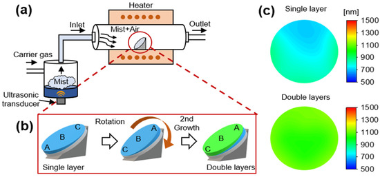
Figure 1.
(a) Schematic of a horizontal hot-wall mist chemical vapor deposition (CVD). (b) Experimental procedure for the fabrication of the single- and double-layer growth. A (at the primary flat of the substrate), B (at the center of the substrate), and C (at opposite position from A) points indicate the orientation of the substrate in the reactor. (c) The thickness distributions of the single-layer and double-layer samples.
According to previous studies [15,24], fabricating a Ga2O3 layer by the conventional horizontal hot-wall mist CVD exhibits a poor thickness uniformity, which resulted in a sloped single layer (Figure 1b). Hence, we developed a two-step growth process with an initial idea of improving the thickness uniformity. In the two-step growth process, first, the substrate was taken out of the reactor after the conventional growth (the first step), after which the substrate was rotated 180°, loaded back to the furnace, and deposited for the second layer (the second step) to achieve improved thickness uniformity in the double Ga2O3 layers (Figure 1b). The growth conditions and time for the first and second steps are exactly the same.
The thickness of the grown layers was measured using spectral reflectometry (F20-UV, FILMETRICS, San Diego, CA, USA). The thickness of the grown layers was verified using field-emission scanning electron microscopy (FE-SEM; JSM-7610F, JEOL, Tokyo, Japan), and the crystal structure of the grown layers was investigated using X-ray diffraction (XRD) with a Cu Kα1 radiation (λ = 1.54056 Å). An ω-scan was performed using high-resolution XRD (SMARTLAB, Rigaku, Tokyo, Japan) to examine the crystal quality. The surface roughness of the grown epilayer was investigated using atomic force microscopy (AFM; JSPM-5200, JEOL, Tokyo, Japan), and the dislocation in the grown layers was investigated using transmission electron microscopy (TEM; Themis Z, Thermo Fisher Scientific, Waltham, MA, USA). The mobility and carrier concentration of the sample were examined using Hall measurement systems at low temperatures (HMS-5000, ECOPiA, Anyang, Korea) and at room temperature (HMS-2000, ECOPiA, Anyang, Korea). The injection current of the Hall measurement was set in the range of 10–100 µA with a magnetic field of 0.52 T.
3. Results and Discussion
3.1. Microstructural Gradation of the Ga2O3 Layers
Figure 1c shows the thickness distribution contour maps of the grown Ga2O3 layers at a growth time of 120 min. The thickness of the single Ga2O3 layer over the substrate ranged from 700 to 900 nm. As reported in previous studies [15,24], the thickness of the grown Ga2O3 layers reduces from the lower to the upper position of the substrate, owing to the increase in the velocity of the mist flow during the horizontal mist CVD. In contrast, the thickness of the double Ga2O3 layers over the substrate was in the range of 1055 ± 85 nm, indicating a high thickness uniformity. The cross-sectional SEM images of the areas around the center of the substrates (position B) of the single and double Ga2O3 layers are shown in Figure 2a. Owing to the relative smoothness of the grown layers, the actual growth thickness was consistent with the values obtained by spectral reflectometry. Hence, the double layers exhibited improved thickness uniformity. Figure 2b shows the 2θ XRD scan of the Ga2O3 layers grown on a c-plane sapphire substrate. The (0006) plane peaks of sapphire and α-Ga2O3 were simultaneously observed at 41.67 and 40.25° in the XRD patterns of the single and double layers, respectively [25]. In addition, the diffraction pattern of the double Ga2O3 layers observed along the ⟨⟩ zone axis further confirmed the corundum structure of the α-Ga2O3 crystal with TEM analysis.
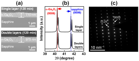
Figure 2.
(a) Cross-sectional field emission scanning electron microscopy (FE-SEM) images and thickness of the single layer and double layers samples grown for 120 min. (b) 2θ-scan X-ray diffraction (XRD) patterns of the samples. (c) Electron diffraction pattern of the double layers sample.
Figure 3 shows the AFM images of the single and double Ga2O3 layers at different substrate positions (A, B, and C). Figure 3 shows the three-dimensional AFM images of the layers with an area of 5 µm × 5 µm. In addition to the change in the layer thickness, the single Ga2O3 layer exhibited a significantly varying surface roughness. The root mean square (RMS) surface roughness of positions A, B, and C were 14.9, 11.6, and 8.3 nm for the single Ga2O3 layer, and 7.9, 8.0, and 7.5 nm for the double Ga2O3 layer, respectively. The standard deviation of the RMS surface roughness of the single Ga2O3 layer was as large as 3.3 nm, which is predictable for a single epitaxial layer prepared by the horizontal mist CVD [24]. However, the standard deviation of the RMS surface roughness was 0.3 nm for the double Ga2O3 layer, indicating the uniform surface roughness of the double Ga2O3 layers. Hence, the two-step growth significantly improves the roughness uniformity of the final Ga2O3 epitaxial layer.
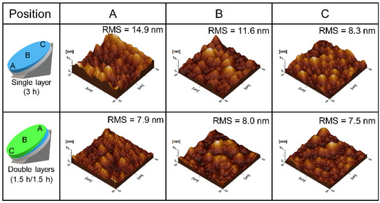
Figure 3.
Roughness of the single- and double-layer samples at different positions (A–C).
Figure 4a shows the plot of the RMS surface roughness of the Ga2O3 layers with a change in the thickness. At first glance, the overall RMS surface roughness of the Sn-doped Ga2O3 layers fabricated in this study were several times higher than that of unintentionally-doped Ga2O3 layers reported in a previous study (0.8–3.7 nm) [24]. It was explained by the segregation of Sn dopants during growth, which increases significantly under a Ga-rich VI/III ratio [26]. Moreover, the RMS values of both the single and double Ga2O3 layers increased with the thickness of the grown layer. The double Ga2O3 layers exhibited a more notable improved smoothness compared to the single Ga2O3 layer. These results indicate that the two-step growth with a substrate rotation of 180° was effective for improving the uniformity of the substrate and surface morphology (Figure 4b).
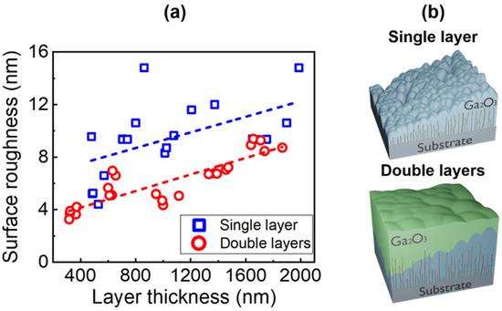
Figure 4.
(a) Dependence of the surface roughness on the epitaxial layer thickness. (b) Schematic of the structural growth behaviors of the single layer and double layers.
3.2. Crystal Quality
Figure 5 shows the full width at half maximum (FWHM) plots of the ω-scan XRD rocking curve of the symmetrical (0006) and asymmetrical (104) planes as a function of the Ga2O3 layer thickness. Both the single and double Ga2O3 layers maintained relatively low FWHMs values for the symmetrical (0006) plane reflection over the entire thickness, which ranged from 40–90 arcsec, indicating the highly preferred crystal orientation of the layers along the surface normal direction (i.e., growth direction). In contrast, the FWHM values of the asymmetric (104) plane reflections were relatively higher than those of the (0006) plane. As the thickness of the layers increased, the FWHMs of the (104) plane reflections rapidly decreased and was saturated to ≈1000 arcsec at a certain thickness (e.g., ≈1.5 µm). The large discrepancy in the FWHM values of the and planes are commonly attributed to the edge and screw dislocations density, respectively, wherein the edge dislocation density is relatively higher than the screw dislocation density [27]. This indicates that the improved crystallinity of the epitaxial layers could be attributed to the reduction in the edge dislocation density with an increase in the thickness until saturation. The reduction in the edge dislocation was further confirmed by the TEM analysis of the area along the ⟨⟩ zone axis in the upper panel of Figure 5a,b. To observe the full variation over the growth thickness, ≈1700-nm-grown Ga2O3 layers of both the single and double Ga2O3 layers were selected. Owing to the growth of homoepitaxial layers in the double Ga2O3 layers, the interface between the two layers in the double Ga2O3 layers was not observed. In addition, dense dark lines were observed at the interface of the Ga2O3 layer and sapphire substrates, indicating the occurrence of a high density of threading dislocations at the initial growth stage. As the growth proceeded, the dislocation density of the single and double Ga2O3 layers decreased. This indicates that the reduction in the edge dislocations resulted in a high crystal quality of the Ga2O3 layers with an increase in the growth thickness. In summary, the improvement in the crystal quality on the FWHM plane XRD rocking curve was similarly saturated at certain thicknesses by thickening both the single and double Ga2O3 layers (≈1.2 and ≈1.0 µm, respectively). The Hall measurement at room temperature (RT) was conducted for investigating the electrical properties of the single and double layers. For both of them, the low-quality, thin Ga2O3 layers are unable to measure the Hall’s effect at RT, whereas the high-quality, thick Ga2O3 layers are able to measure the Hall’s effect. Therefore, the grown Ga2O3 layers were divided into three zones depending on the crystal quality and Hall measurability at RT as follows:
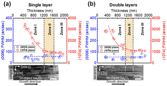
Figure 5.
Full width at half maximum values of the two layers as a function of the Ga2O3 epitaxial thickness of the: (a) single-layer and (b) double-layer samples. The transmission electron microscopy (TEM) images show the propagation of edge dislocation associated with the FWHM.
- Zone I: Thin layer (<1.1 µm), Hall effect unmeasurable at RT, low crystal quality.
- Zone II: Transition layer, Hall effect unmeasurable, saturated crystal quality.
- Zone III: Thick layer (>1.6 µm), Hall effect measurable at RT, high crystal quality.
The largest discrepancy between the single and double Ga2O3 layers was observed at the transition layer (Zone II). The thickness of the transition layer of the single Ga2O3 layer was in the range from 1.2–1.6 µm. Despite the saturation of the enhancement in the crystal quality, the single, one-step growth required a further elongation of the high-quality region. In contrast, the thickness of the transition layer of the double Ga2O3 layers ranged from 1.1–1.4 µm. Compared to the single Ga2O3 layer, the thickness of the double Ga2O3 layer left-shifted and reduced, indicating that the Hall effect was measurable before the double Ga2O3 layer reached the highest crystal quality. This indicates that a high-quality, conductive Ga2O3 layer is achievable at a relatively low thickness using the two-step growth procedure, suggesting an advantage of the two-step growth method compared to the one-step growth method. The origin of the measurability discrepancy of both layers are discussed in the next section.
3.3. Electrical Properties and Scattering Mechanism
Figure 6 shows the result of the temperature-dependent Hall measurement of the layers in the range from 80–300 K. The carrier concentrations and mobilities of the two-inch Ga2O3 epilayers were obtained at three different positions (A, B, and C). A similar thickness of ≈1.7 µm, including a high crystal quality region (Zone III), was selected to minimize the dislocation scattering as the specimen of both the single and double Ga2O3 layers. The temperature-dependent carrier concentration of the single and double Ga2O3 layers is shown in Figure 6a,b, respectively. The spatial distribution of the carrier concentration was significantly inhomogeneous depending on the position of the substrate. At a low position in the single Ga2O3 layer (i.e., point A for the single layer), the carrier concentration (≈1 × 1019 cm−3) was almost one order higher than those of other positions (≈1 × 1018 cm−3), as shown in Figure 6a. This high carrier concentration exhibited an almost constant distribution over the entire temperature range owing to the degenerate tendency of free carriers [19]. The same distribution behavior of the temperature-dependent carrier concentration was observed in the double Ga2O3 layers (Figure 6b). Among the three positions, the lowest position (i.e., position C) of the double Ga2O3 layers exhibited the highest carrier concentration. In addition, compared to the single layer (≈1 × 1019 cm−3), the double layer exhibited a slightly lower maximum carrier concentration (≈5 × 1018 cm−3). The concentration of the other positions (i.e., positions A and B) was almost constant at ≈1 × 1018 cm−3. It suggests that the inhomogeneous carrier distribution is inevitable in the horizontal mist CVD system with an inclined substrate holder because of inhomogeneous dopant concentration. The mist flow was highly stagnant at the lower position of the substrate [24], creating a higher doping efficiency at that position. It implies that a low mist flow velocity can increase the doping efficiency. Moreover, the spatial gradient of the carrier concentration was strongly affected by Sn concentration distribution at the surface, regardless of the Sn concentration distribution of the underlying layer.
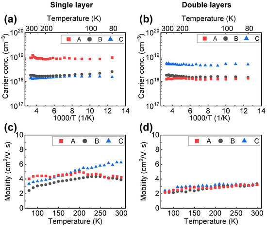
Figure 6.
Temperature-dependent carrier concentrations and mobilities of the (a,c) single layer and (b,d) double layers of Sn-doped α-Ga2O3. The average thicknesses of those samples are 1700 nm. A, B, and C are positions located near the wafer flat, center, and edge of the wafer, respectively (see Figure 1).
The mobility distribution of the single and double Ga2O3 layers over the entire temperature range is shown in Figure 6c,d. Regardless of the maximum carrier concentration, position A on the single Ga2O3 layer exhibited the largest mobility in the low-temperature range of 80–150 K (Figure 6c). According to Matthiessen’s rule, the accumulated mobility µ is defined by the components mobility as described in Equation (1):
where T, µc, µp, and µs are temperature, Coulomb scattering mobility, phonon scattering mobility, and surface roughness scattering, respectively [19,20]. The dislocation scattering was excluded in Zone III, where the dislocation was small and crystal quality was high (See also the schematic descriptions of the mobility variation depending on scattering effects in Figure S1a, Supplementary Materials) [22,28]. Therefore, high mobility at position A could be attributed to the higher effective thickness and high crystal quality at that position compared to other positions, which were susceptible to low dislocation scattering. Moreover, Coulomb scattering at low temperatures and phonon scattering at high temperatures are proportionally related to T3/2 and T−3/2. Hence, the maximum point in position B of the single layer over the whole temperature was observed at 220 K, then the mobility decreases due to phonon scattering. Owing to the maximum carrier concentration of position A on the single Ga2O3 layer, the maximum point shifted to a lower temperature of 200 K and the mobility variation was smaller than that of position B. In contrast, the mobility peak of position C shifted to the higher temperature (300 K) with the highest value of 6.5 cm2/V∙s. As position C of the single Ga2O3 layer exhibited the lowest carrier concentration, the peak shifting behavior to higher temperatures can be considered reasonable. Furthermore, the smooth surface roughness of position C (RMS surface roughness ≈8.3 nm) could result in a sizeable difference from that of position B (RMS surface roughness ≈11.6 nm) on the single Ga2O3 layer, suggesting that the surface roughness scattering considerably influences the carrier mobility in the single Ga2O3 layer [22,29].
1/µ = 1/µc + 1/µp+ 1/µs
In contrast, the carrier mobility of the double Ga2O3 layers slightly and monotonically increased as the temperature increased (Figure 6d). The carrier mobility gradually increased from ≈2 cm2/V∙s and peaked at ≈2.5 cm2/V∙s, which was similarly obtained at 300 K for all three positions. With the layer thickness of 1.7 μm, the crystal quality and surface roughness of the double Ga2O3 layers were good and uniform on all three positions. Therefore, the dislocation and surface roughness scattering could not affect the temperature-dependent characteristics of carrier mobility in the double Ga2O3 layer. On the other hand, the double Ga2O3 layers were susceptible to strong Coulomb scattering owing to the heavily n-doped Ga2O3 (1 × 1019 cm−3) and, consequently, just slightly increased the mobility with temperature. Moreover, the double layers seem to be less affected by phonon scattering and are promising for working at elevated temperatures. Hence, achieving a high electron mobility with lightly doped n-Ga2O3 layers is essential for the Ga2O3-based device applications.
4. Conclusions
In summary, Sn-doped Ga2O3 epitaxial layers were grown on a two-inch sapphire substrate using horizontal mist CVD. The microstructural gradational properties, such as thickness, surface morphology, and dislocation density, of single- and double-grown Ga2O3 layers were compared. The single Ga2O3 layer exhibited a considerable microstructural gradation, which could be attributed to the spatial difference in the flow of mist to the substrates. The bottom of the single Ga2O3 layer exhibited a higher thickness and surface roughness, whereas the upper positions of the substrates exhibited gradually reduced thickness and surface roughness. The microstructural gradational properties of the single Ga2O3 layer resulted in significant deviation in the electrical properties of the layer in terms of carrier concentration and mobility. In contrast, the double Ga2O3 layers exhibited excellent thickness uniformity, surface roughness, and crystal quality compared to the single Ga2O3 layer. Nevertheless, the electron mobility of the double Ga2O3 layers was ≈2.5 cm2/Vs with small variations over a wide range of temperature. These results indicate that the carrier mobility of Ga2O3 layers can be improved with lightly-doped n-Ga2O3 layers. Therefore, the two-step mist CVD growth can prepare a high and homogeneous quality Ga2O3 epitaxial layer for high-temperature and high-power applications.
Supplementary Materials
The following supporting information can be downloaded at: https://www.mdpi.com/article/10.3390/ma15031050/s1, Figure S1: Schematic description of the temperature-dependent carrier mobility of the grown layers under the effects of various scattering mechanisms. Figure S2: Omega-scan XRD patterns and FWHM of (0006) and (104) planes for single and double layers with different thicknesses. Table S1: Hall measurement data of the temperature-dependent carrier mobility and carrier concentration of single and double layers.
Author Contributions
Conceptualization, K.-H.K. and S.-Y.B.; methodology, K.-H.K.; software, K.-H.K. and M.-T.H.; validation, M.-T.H. and S.-Y.B.; formal analysis, K.-H.K., M.-T.H. and M.K.; investigation, K.-H.K. and M.-T.H.; writing—original draft preparation, K.-H.K. and M.-T.H.; writing—review and editing, S.-Y.B.; visualization, K.-H.K. and M.-T.H.; supervision, H.L., O.N., Y.-J.S., S.-M.J. and S.-Y.B.; project administration, Y.-J.S., S.-M.J. and S.-Y.B.; funding acquisition, Y.-J.S., S.-M.J. and S.-Y.B. All authors have read and agreed to the published version of the manuscript.
Funding
This research was supported by the National Research Foundation of Korea (NRF), which is funded by the Ministry of Education (NRF-2021M3H4A3A01061782), and the Ceramic Strategic Research Program (KPP20001) through the Korea Institute of Ceramic Engineering and Technology (KICET) and Ministry of Trade, Industry and Energy (MOTIE), Republic of Korea.
Institutional Review Board Statement
Not applicable.
Informed Consent Statement
Not applicable.
Data Availability Statement
Data is contained within the article.
Conflicts of Interest
The authors declare no conflict of interest.
References
- Pearton, S.J.; Yang, J.; Cary, P.H.; Ren, F.; Kim, J.; Tadjer, M.J.; Mastro, M.A. A Review of Ga2O3 Materials, Processing, and Devices. Appl. Phys. Rev. 2018, 5, 011301. [Google Scholar] [CrossRef] [Green Version]
- Tsao, J.Y.; Chowdhury, S.; Hollis, M.A.; Jena, D.; Johnson, N.M.; Jones, K.A.; Kaplar, R.J.; Rajan, S.; Van de Walle, C.G.; Bellotti, E.; et al. Ultrawide-Bandgap Semiconductors: Research Opportunities and Challenges. Adv. Electron. Mater. 2018, 4, 1600501. [Google Scholar] [CrossRef] [Green Version]
- Fujita, S. Wide-Bandgap Semiconductor Materials: For Their Full Bloom. Jpn. J. Appl. Phys. 2015, 54, 030101. [Google Scholar] [CrossRef] [Green Version]
- Shenai, K.; Scott, R.S.; Baliga, B.J. Optimum Semiconductors for High-Power Electronics. IEEE Trans. Electron Devices 1989, 36, 1811–1823. [Google Scholar] [CrossRef]
- Shenai, K. Future Prospects of Widebandgap (WBG) Semiconductor Power Switching Devices. IEEE Trans. Electron Devices 2015, 62, 248–257. [Google Scholar] [CrossRef]
- Razeghi, M. Short-Wavelength Solar-Blind Detectors-Status, Prospects, and Markets. Proc. IEEE 2002, 90, 1006–1014. [Google Scholar] [CrossRef]
- Mastro, M.A.; Kuramata, A.; Calkins, J.; Kim, J.; Ren, F.; Pearton, S.J. Perspective—Opportunities and Future Directions for Ga2O3. ECS J. Solid State Sci. Technol. 2017, 6, P356. [Google Scholar] [CrossRef]
- Higashiwaki, M.; Sasaki, K.; Kuramata, A.; Masui, T.; Yamakoshi, S. Gallium Oxide (Ga2O3) Metal-Semiconductor Field-Effect Transistors on Single-Crystal β-Ga2O3 (010) Substrates. Appl. Phys. Lett. 2012, 100, 013504. [Google Scholar] [CrossRef]
- Bae, S.-Y. Growth of Various Phases of Gallium Oxide. In Digital Encyclopedia of Applied Physics; John Wiley & Sons, Ltd.: Hoboken, NJ, USA, 2021; pp. 1–37. ISBN 978-3-527-60043-4. [Google Scholar]
- Guo, D.; Guo, Q.; Chen, Z.; Wu, Z.; Li, P.; Tang, W. Review of Ga2O3-Based Optoelectronic Devices. Mater. Today Phys. 2019, 11, 100157. [Google Scholar] [CrossRef]
- Oshima, Y.; Víllora, E.G.; Shimamura, K. Halide Vapor Phase Epitaxy of Twin-Free α-Ga2O3 on Sapphire (0001) Substrates. Appl. Phys. Express 2015, 8, 055501. [Google Scholar] [CrossRef]
- Oshima, T.; Okuno, T.; Fujita, S. Ga2O3 Thin Film Growth on c-Plane Sapphire Substrates by Molecular Beam Epitaxy for Deep-Ultraviolet Photodetectors. Jpn. J. Appl. Phys. 2007, 46, 7217. [Google Scholar] [CrossRef]
- Son, H.; Choi, Y.-J.; Hwang, J.; Jeon, D.-W. Influence of Post-Annealing on Properties of α-Ga2O3 Epilayer Grown by Halide Vapor Phase Epitaxy. ECS J. Solid State Sci. Technol. 2019, 8, Q3024. [Google Scholar] [CrossRef]
- Oka, D.; Fukumura, T. Crystal Engineering for Novel Functionalities with Oxide Thin Film Epitaxy. CrystEngComm 2017, 19, 2144–2162. [Google Scholar] [CrossRef]
- Kim, K.-H.; Ha, M.-T.; Kwon, Y.-J.; Lee, H.; Jeong, S.-M.; Bae, S.-Y. Growth of 2-Inch α-Ga2O3 Epilayers via Rear-Flow-Controlled Mist Chemical Vapor Deposition. ECS J. Solid State Sci. Technol. 2019, 8, Q3165. [Google Scholar] [CrossRef]
- Shinohara, D.; Fujita, S. Heteroepitaxy of Corundum-Structured α-Ga2O3 Thin Films on α-Al2O3 Substrates by Ultrasonic Mist Chemical Vapor Deposition. Jpn. J. Appl. Phys. 2008, 47, 7311. [Google Scholar] [CrossRef]
- Kawaharamura, T.; Dang, G.T.; Furuta, M. Successful Growth of Conductive Highly Crystalline Sn-Doped α-Ga2O3 Thin Films by Fine-Channel Mist Chemical Vapor Deposition. Jpn. J. Appl. Phys. 2012, 51, 040207. [Google Scholar] [CrossRef]
- Kaneko, K.; Kawanowa, H.; Ito, H.; Fujita, S. Evaluation of Misfit Relaxation in α-Ga2O3 Epitaxial Growth on α-Al2O3 Substrate. Jpn. J. Appl. Phys. 2012, 51, 020201. [Google Scholar] [CrossRef]
- Akaiwa, K.; Kaneko, K.; Ichino, K.; Fujita, S. Conductivity Control of Sn-Doped α-Ga2O3 Thin Films Grown on Sapphire Substrates. Jpn. J. Appl. Phys. 2016, 55, 1202BA. [Google Scholar] [CrossRef] [Green Version]
- Ng, H.M.; Doppalapudi, D.; Moustakas, T.D.; Weimann, N.G.; Eastman, L.F. The Role of Dislocation Scattering in n-Type GaN Films. Appl. Phys. Lett. 1998, 73, 821–823. [Google Scholar] [CrossRef]
- Ueda, N.; Hosono, H.; Waseda, R.; Kawazoe, H. Anisotropy of Electrical and Optical Properties in β-Ga2O3 Single Crystals. Appl. Phys. Lett. 1997, 71, 933–935. [Google Scholar] [CrossRef]
- Shin, H.; Lim, K.; Hwang, S.; Han, I.-K.; Jang, M. The Evaluation of Hole Mobility Characteristics with Surface Roughness. J. Nanosci. Nanotechnol. 2017, 17, 7766–7770. [Google Scholar] [CrossRef]
- Ha, M.-T.; Kim, K.-H.; Shin, Y.-J.; Jeong, S.-M.; Bae, S.-Y. Leidenfrost Motion of Water Microdroplets on Surface Substrate: Epitaxy of Gallium Oxide via Mist Chemical Vapor Deposition. Adv. Mater. Interfaces 2021, 8, 2001895. [Google Scholar] [CrossRef]
- Ha, M.-T.; Kim, K.-H.; Kwon, Y.-J.; Kim, C.-J.; Jeong, S.-M.; Bae, S.-Y. Understanding Thickness Uniformity of Ga2O3 Thin Films Grown by Mist Chemical Vapor Deposition. ECS J. Solid State Sci. Technol. 2019, 8, Q3206. [Google Scholar] [CrossRef]
- Zhang, J.; Shi, J.; Qi, D.-C.; Chen, L.; Zhang, K.H.L. Recent Progress on the Electronic Structure, Defect, and Doping Properties of Ga2O3. APL Mater. 2020, 8, 020906. [Google Scholar] [CrossRef] [Green Version]
- Sasaki, K.; Yamakoshi, S.; Kuramata, A. Ozone-Enhanced Molecular Beam Epitaxy. In Gallium Oxide: Materials Properties, Crystal Growth, and Devices; Higashiwaki, M., Fujita, S., Eds.; Springer Series in Materials Science; Springer International Publishing: Cham, Switzerland, 2020; pp. 123–140. ISBN 978-3-030-37153-1. [Google Scholar]
- Ma, T.C.; Chen, X.H.; Kuang, Y.; Li, L.; Li, J.; Kremer, F.; Ren, F.-F.; Gu, S.L.; Zhang, R.; Zheng, Y.D.; et al. On the Origin of Dislocation Generation and Annihilation in α-Ga2O3 Epilayers on Sapphire. Appl. Phys. Lett. 2019, 115, 182101. [Google Scholar] [CrossRef]
- Noguchi, M.; Iwamatsu, T.; Amishiro, H.; Watanabe, H.; Kita, K.; Yamakawa, S. Determination of Intrinsic Phonon-Limited Mobility and Carrier Transport Property Extraction of 4H-SiC MOSFETs. In Proceedings of the 2017 IEEE International Electron Devices Meeting (IEDM), San Francisco, CA, USA, 2–6 December 2017; pp. 9.3.1–9.3.4. [Google Scholar]
- Böer, K.W.; Pohl, U.W. Carrier Scattering at Low Electric Fields. In Semiconductor Physics; Böer, K.W., Pohl, U.W., Eds.; Springer International Publishing: Cham, Switzerland, 2018; pp. 897–930. ISBN 978-3-319-69150-3. [Google Scholar]
Publisher’s Note: MDPI stays neutral with regard to jurisdictional claims in published maps and institutional affiliations. |
© 2022 by the authors. Licensee MDPI, Basel, Switzerland. This article is an open access article distributed under the terms and conditions of the Creative Commons Attribution (CC BY) license (https://creativecommons.org/licenses/by/4.0/).