

Optimization of Sputtering Process for Medium Entropy Alloy Nanotwinned CoCrFeNi Thin Films by Taguchi Method


Abstract
1. Introduction
2. Experimental Methods
2.1. Sample Preparation
2.2. S/N Ratio Analysis and Analysis of Variance (ANOVA)
2.3. Characterization Methods
3. Results and Discussion
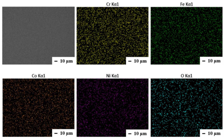
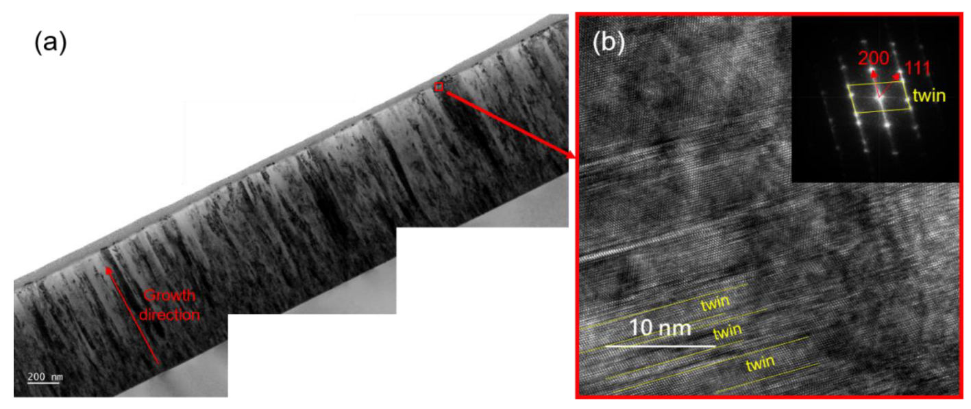
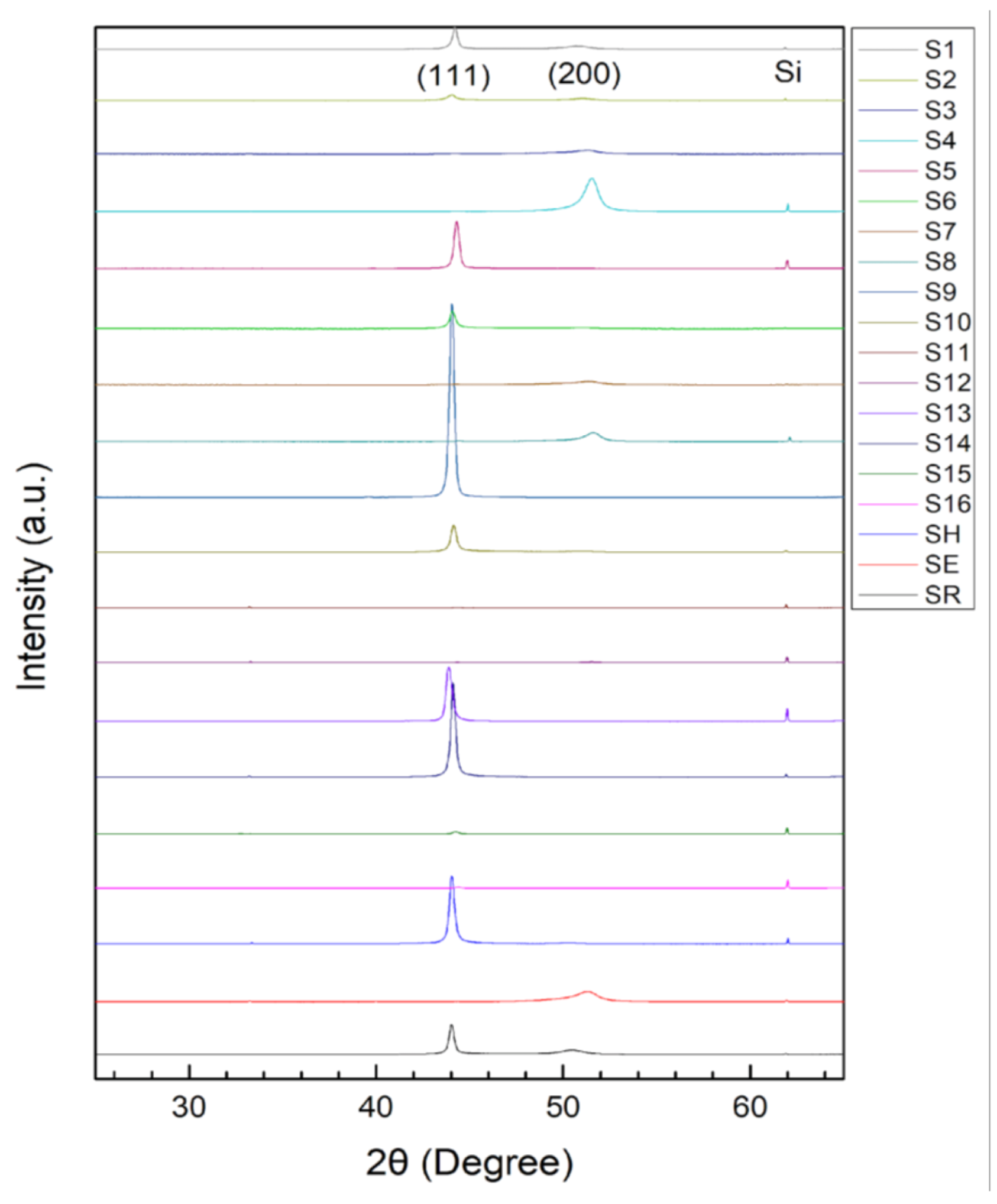
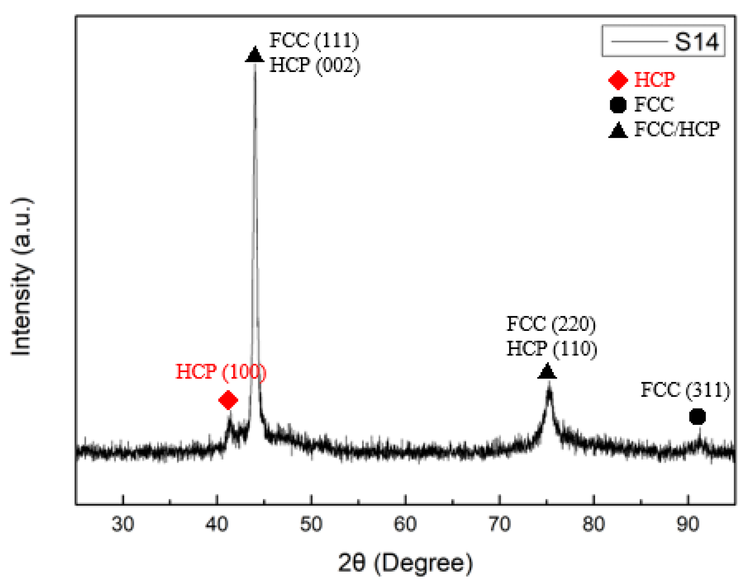
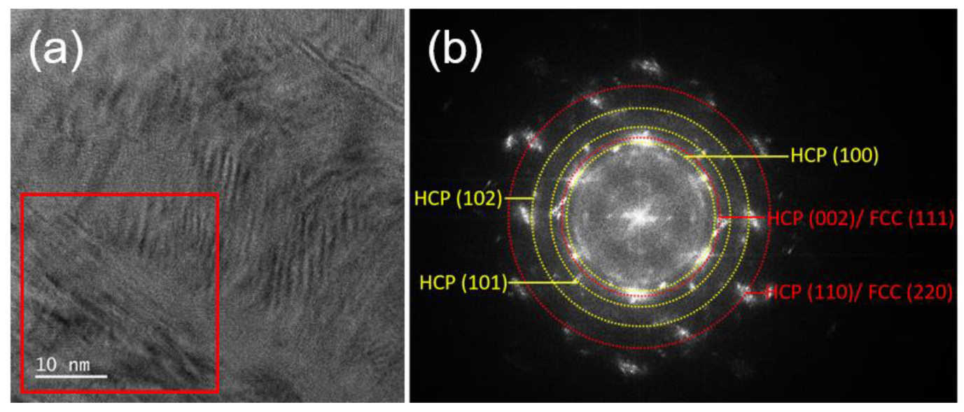
3.1. Characteristics of CoCrFeNi Thin Films
3.2. Optimization of Film Properties
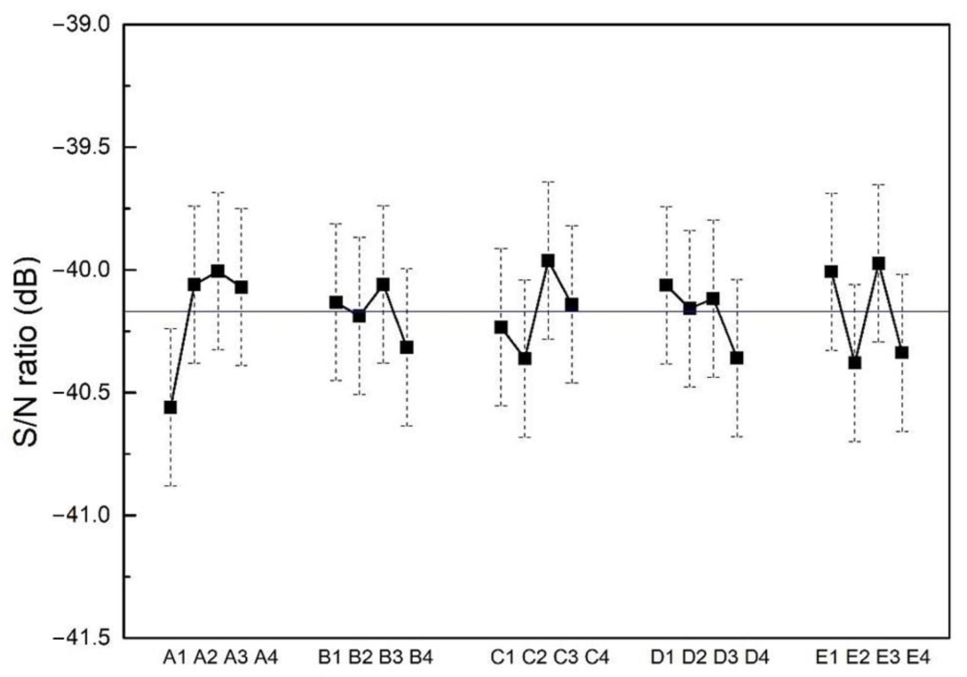
3.2.1. Resistivity
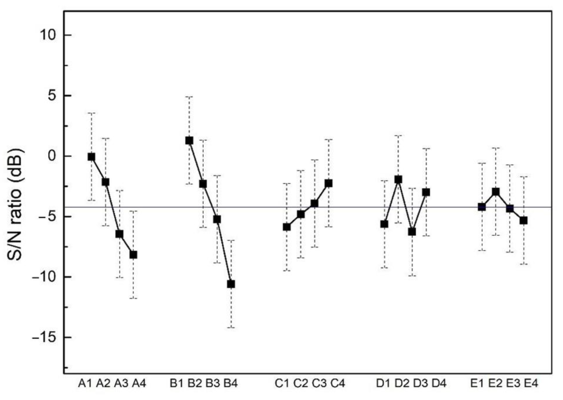
3.2.2. Surface Roughness
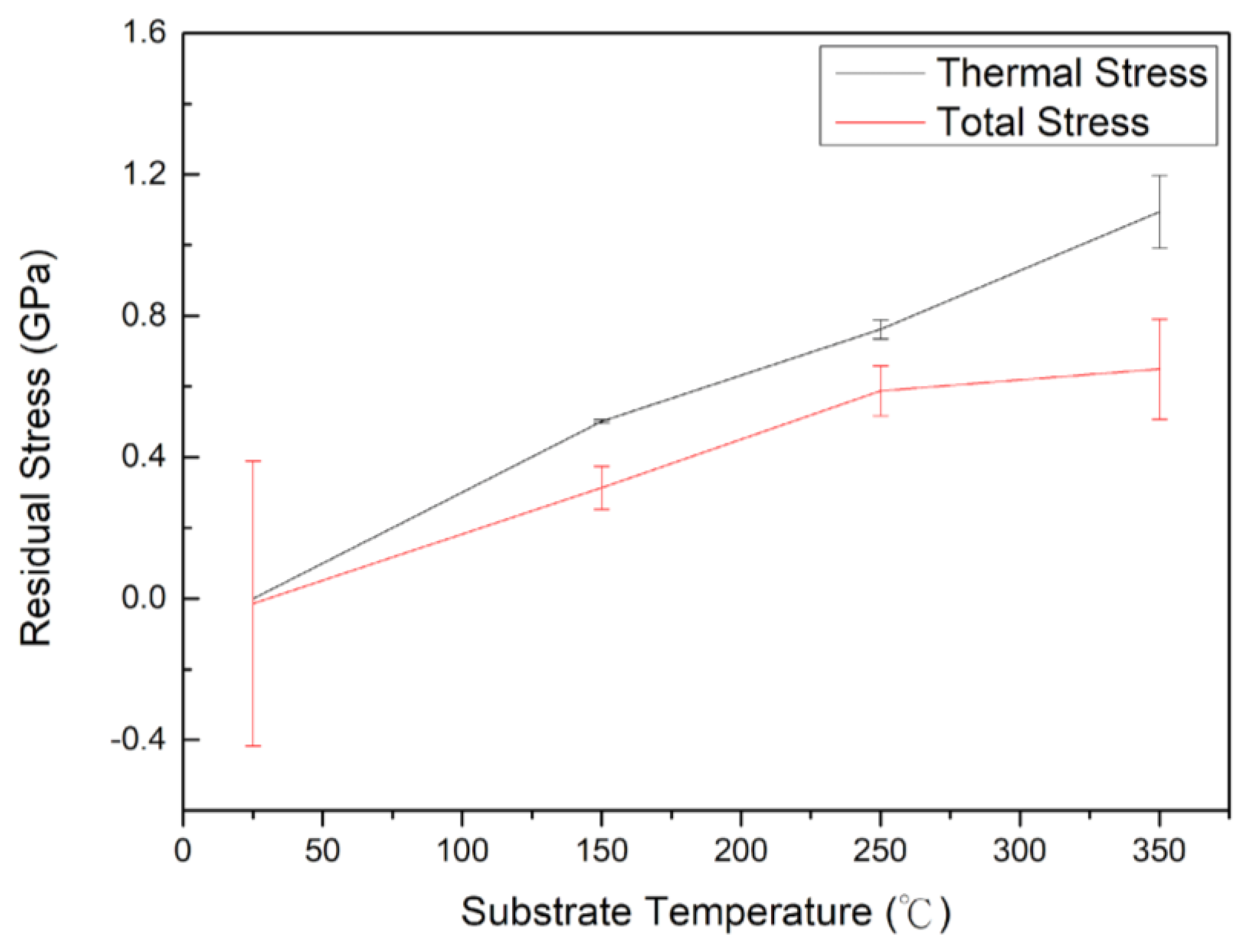
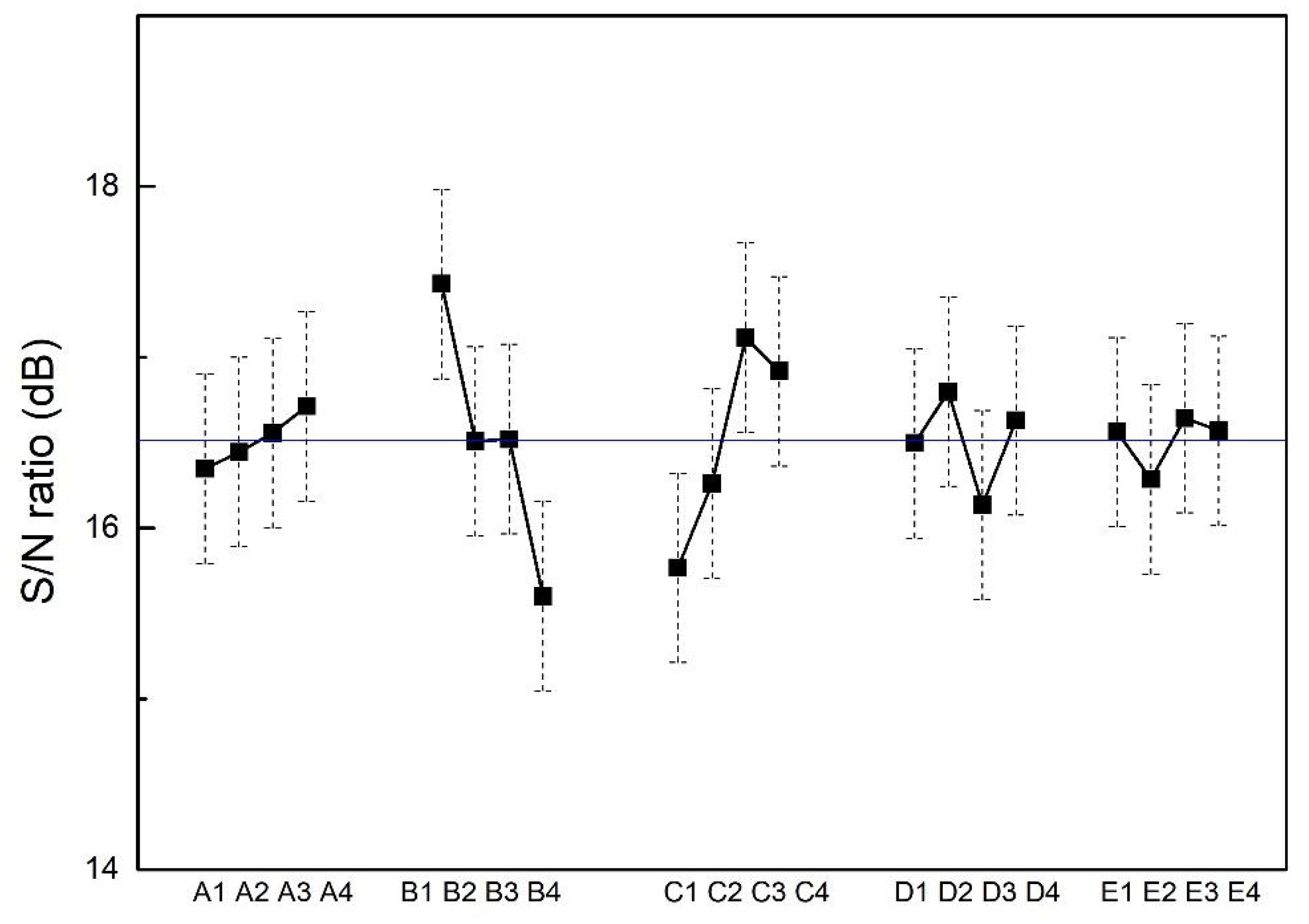
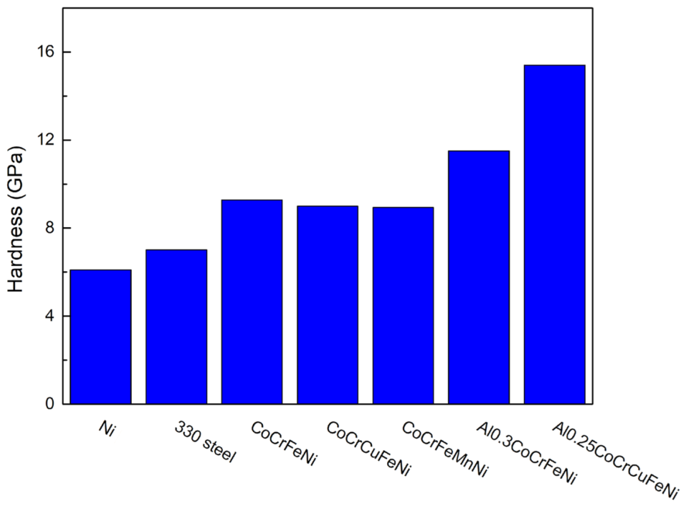
3.2.3. Mechanical Strength
4. Conclusions
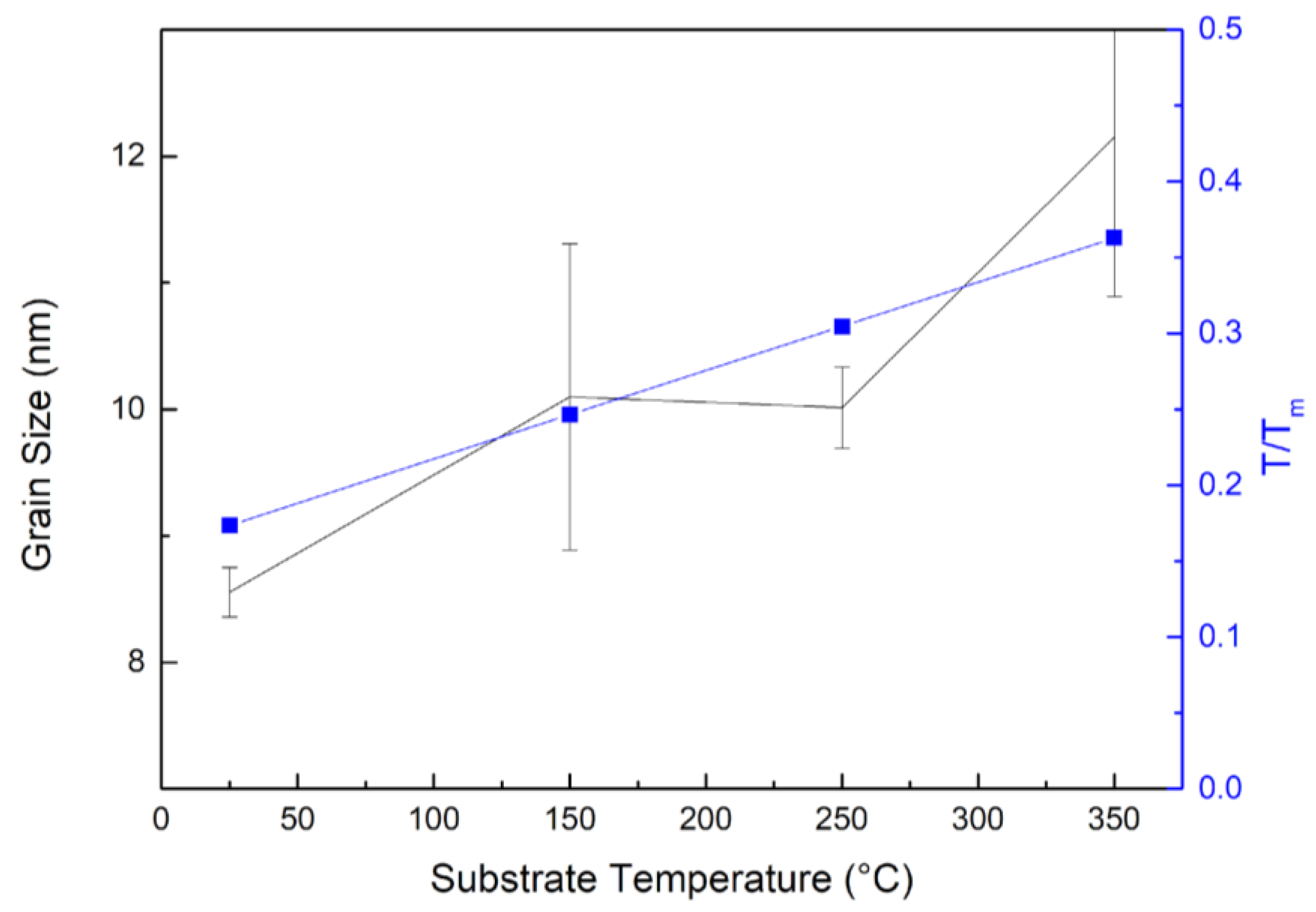
- Among these five factors, substrate bias was the most sensitive factor to electrical resistivity, whereas substrate temperature was dominant in terms of influencing the surface roughness and hardness, which may be attributed to the greater grain size enhanced by elevated temperature.
- The optimized parameters for low electrical resistivity (98.2 ± 0.7 μΩ∙cm), low surface roughness (0.5 ± 0.0 nm) and high hardness (9.3 ± 0.2 GPa) were achieved.
- Dual FCC and HCP phases were found locally in CoCrFeNi thin films, because the energy provided from the sputtering system and additional applied substrate bias may facilitate the atoms to overcome the barrier of FCC-HCP phase transformation.
Author Contributions
Funding
Institutional Review Board Statement
Informed Consent Statement
Data Availability Statement
Acknowledgments
Conflicts of Interest
References
- Yeh, J.W.; Chen, S.-K.; Lin, S.-J.; Gan, J.-Y.; Chin, T.-S.; Shun, T.-T.; Tsau, C.-H.; Chang, S.-Y. Nanostructured high-entropy alloys with multiple principal elements: Novel alloy design concepts and outcomes. Adv. Eng. Mater. 2004, 6, 299–303. [Google Scholar] [CrossRef]
- Otto, F.; Dlouhý, A.; Somsen, C.; Bei, H.; Eggeler, G.; George, E.P. The influences of temperature and microstructure on the tensile properties of a CoCrFeMnNi high-entropy alloy. Acta Mater. 2013, 61, 5743–5755. [Google Scholar] [CrossRef]
- Shi, Y.; Yang, B.; Liaw, P. Corrosion-Resistant High-Entropy Alloys: A Review. Metals 2017, 7, 43. [Google Scholar] [CrossRef]
- Luo, H.; Li, Z.; Mingers, A.M.; Raabe, D. Corrosion behavior of an equiatomic CoCrFeMnNi high-entropy alloy compared with 304 stainless steel in sulfuric acid solution. Corros. Sci. 2018, 134, 131–139. [Google Scholar] [CrossRef]
- Gludovatz, B.; Hohenwarter, A.; Catoor, D.; Chang, E.H.; George, E.P.; Ritchie, R.O. A fracture-resistant high-entropy alloy for cryogenic applications. Science 2014, 345, 1153–1158. [Google Scholar] [CrossRef] [PubMed]
- Ye, Y.; Wang, Q.; Lu, J.; Liu, C.; Yang, Y. High-entropy alloy: Challenges and prospects. Mater. Today 2016, 19, 349–362. [Google Scholar] [CrossRef]
- Schuh, B.; Mendez-Martin, F.; Völker, B.; George, E.P.; Clemens, H.; Pippan, R.; Hohenwarter, A. Mechanical properties, microstructure and thermal stability of a nanocrystalline CoCrFeMnNi high-entropy alloy after severe plastic deformation. Acta Mater. 2015, 96, 258–268. [Google Scholar] [CrossRef]
- Zhang, H.; Xu, W.; Xu, Y.; Lu, Z.; Li, D. The thermal-mechanical behavior of WTaMoNb high-entropy alloy via selective laser melting (SLM): Experiment and simulation. Int. J. Adv. Manuf. Technol. 2018, 96, 461–474. [Google Scholar] [CrossRef]
- George, E.P.; Curtin, W.A.; Tasan, C.C. High entropy alloys: A focused review of mechanical properties and deformation mechanisms. Acta Mater. 2020, 188, 435–474. [Google Scholar] [CrossRef]
- Wu, P.; Gan, K.; Yan, D.; Fu, Z.; Li, Z. A non-equiatomic FeNiCoCr high-entropy alloy with excellent anti-corrosion performance and strength-ductility synergy. Corros. Sci. 2021, 183, 109341. [Google Scholar] [CrossRef]
- Senkov, O.N.; Wilks, G.B.; Scott, J.M.; Miracle, D.B. Mechanical properties of Nb25Mo25Ta25W25 and V20Nb20Mo20Ta20W20 refractory high entropy alloys. Intermetallics 2011, 19, 698–706. [Google Scholar] [CrossRef]
- Jin, G.; Cai, Z.; Guan, Y.; Cui, X.; Liu, Z.; Li, Y.; Dong, M. High temperature wear performance of laser-cladded FeNiCoAlCu high-entropy alloy coating. Appl. Surf. Sci. 2018, 445, 113–122. [Google Scholar] [CrossRef]
- Ye, Q.; Feng, K.; Li, Z.; Lu, F.; Li, R.; Huang, J.; Wu, Y. Microstructure and corrosion properties of CrMnFeCoNi high entropy alloy coating. Appl. Surf. Sci. 2017, 396, 1420–1426. [Google Scholar] [CrossRef]
- Bachani, S.K.; Wang, C.-J.; Lou, B.-S.; Chang, L.-C.; Lee, J.-W. Fabrication of TiZrNbTaFeN high-entropy alloys coatings by HiPIMS: Effect of nitrogen flow rate on the microstructural development, mechanical and tribological performance, electrical properties and corrosion characteristics. J. Alloy. Compd. 2021, 873, 159605. [Google Scholar] [CrossRef]
- Hsiao, Y.-T.; Tung, C.-H.; Lin, S.-J.; Yeh, J.-W.; Chang, S.-Y. Thermodynamic route for self-forming 1.5 nm V-Nb-Mo-Ta-W high-entropy alloy barrier layer: Roles of enthalpy and mixing entropy. Acta Mater. 2020, 199, 107–115. [Google Scholar] [CrossRef]
- Kumar, P.; Avasthi, S. Diffusion barrier with 30-fold improved performance using AlCrTaTiZrN high-entropy alloy. J. Alloy. Compd. 2020, 814, 151755. [Google Scholar] [CrossRef]
- Wang, J.-J.; Ouyang, F.-Y. Nanotwinned medium entropy alloy CoCrFeNi thin films with ultra-high hardness: Modifying residual stress without scarifying hardness through tuning substrate bias. Surf. Coat. Technol. 2022, 434, 128191. [Google Scholar] [CrossRef]
- Wang, B.; He, H.; Naeem, M.; Lan, S.; Harjo, S.; Kawasaki, T.; Nie, Y.; Kui, H.W.; Ungár, T.; Ma, D.; et al. Deformation of CoCrFeNi high entropy alloy at large strain. Scr. Mater. 2018, 155, 54–57. [Google Scholar] [CrossRef]
- Chan, K.W.; Tjong, S.C. Effect of Secondary Phase Precipitation on the Corrosion Behavior of Duplex Stainless Steels. Materials 2014, 7, 5268–5304. [Google Scholar] [CrossRef]
- Huo, W.; Fang, F.; Zhou, H.; Xie, Z.; Shang, J.; Jiang, J. Remarkable strength of CoCrFeNi high-entropy alloy wires at cryogenic and elevated temperatures. Scr. Mater. 2017, 141, 125–128. [Google Scholar] [CrossRef]
- Huo, W.; Zhou, H.; Fang, F.; Hu, X.; Xie, Z.; Jianga, J. Strain-rate effect upon the tensile behavior of CoCrFeNi high-entropy alloys. Mater. Sci. Eng. A 2017, 689, 366–369. [Google Scholar] [CrossRef]
- Hung, P.T.; Kawasaki, M.; Han, J.; Lábár, J.L.; Gubicza, J. Microstructure evolution in a nanocrystalline CoCrFeNi multi-principal element alloy during annealing. Mater. Charact. 2021, 171, 110807. [Google Scholar] [CrossRef]
- Nagy, P.; Rohbeck, N.; Roussely, G.; Sortais, P.; Lábár, J.L.; Gubicza, J.; Michler, J.; Pethöa, L. Processing and characterization of a multibeam sputtered nanocrystalline CoCrFeNi high-entropy alloy film. Surf. Coat. Technol. 2020, 386, 125465. [Google Scholar] [CrossRef]
- Khan, N.A.; Akhavan, B.; Zhou, H.; Chang, L.; Wang, Y.; Sun, L.; Bilek, M.M.; Liu, Z. High entropy alloy thin films of AlCoCrCu0.5FeNi with controlled microstructure. Appl. Surf. Sci. 2019, 495, 143560. [Google Scholar] [CrossRef]
- Sha, C.; Zhou, Z.; Xie, Z.; Munroe, P. High entropy alloy FeMnNiCoCr coatings: Enhanced hardness and damage-tolerance through a dual-phase structure and nanotwins. Surf. Coat. Technol. 2020, 385, 125435. [Google Scholar] [CrossRef]
- Lin, Y.-C.; Hsu, S.-Y.; Song, R.-W.; Lo, W.-L.; Lai, Y.-T.; Tsai, S.-Y.; Duh, J.-G. Improving the hardness of high entropy nitride (Cr0.35Al0.25Nb0.12Si0.08V0.20)N coatings via tuning substrate temperature and bias for anti-wear applications. Surf. Coat. Technol. 2020, 403, 126417. [Google Scholar] [CrossRef]
- Köçkar, H.; Şentürk, Ö. Rotation speed induced properties of quaternary FeNiCrCd thin films easy-prepared from a single magnetron sputtering. Optoelectron. Adv. Mater. Rapid Commun. 2019, 13, 620–623. [Google Scholar]
- Hsiao, Y.-C.; Lee, J.-W.; Yang, Y.-C.; Lou, B.-S. Effects of duty cycle and pulse frequency on the fabrication of AlCrN thin films deposited by high power impulse magnetron sputtering. Thin Solid Film 2013, 549, 281–291. [Google Scholar] [CrossRef]
- Roy, R.K. A Primer on the Taguchi Method, 2nd ed.; Society of Manufacturing Engineers: Southfield, MI, USA, 2010. [Google Scholar]
- Stoney, G.G. The tension of metallic films deposited by electrolysis. Proc. R. Soc. Lond. Ser. A Contain. Pap. A Math. Phys. Character 1909, 82, 172–175. [Google Scholar]
- Shackelford, J.F.; Alexander, W. CRC Materials Science and Engineering Handbook, 3rd ed.; CRC Press: Boca Raton, FL, USA, 2000. [Google Scholar]
- Pharr, G.M. An improved technique for determining hardness and elastic modulus using load and displacement sensing indentation experiments. J. Mater. Res. 1992, 7, 1564–1583. [Google Scholar]
- Guo, S.; Ng, C.; Lu, J.; Liu, C.T. Effect of valence electron concentration on stability of fcc or bcc phase in high entropy alloys. J. Appl. Phys. 2011, 109, 103505. [Google Scholar] [CrossRef]
- Zhang, Y.H.; Zhuang, Y.; Hu, A.; Kai, J.J.; Liu, C.T. The origin of negative stacking fault energies and nano-twin formation in face-centered cubic high entropy alloys. Scr. Mater. 2017, 130, 96–99. [Google Scholar] [CrossRef]
- Liu, Y.; Zheng, G.P. The effects of chemical disorder and external loading conditions on the structural transformation between HCP and FCC phases in CrCoFeNi high-entropy alloys: A first-principles study. Philos. Mag. 2020, 100, 2857–2875. [Google Scholar] [CrossRef]
- Feng, X.B.; Fu, W.; Zhang, J.Y.; Zhao, J.T.; Li, J.; Wu, K.; Liu, G.; Sun, J. Effects of nanotwins on the mechanical properties of Al x CoCrFeNi high entropy alloy thin films. Scr. Mater. 2017, 139, 71–76. [Google Scholar] [CrossRef]
- Chawake, N.; Zálešák, J.; Gammer, C.; Franz, R.; Cordill, M.J.; Tae, J.K.; Eckert, J. Microstructural characterization of medium entropy alloy thin films. Scr. Mater. 2020, 177, 22–26. [Google Scholar] [CrossRef]
- Tian, F.; Varga, L.K.; Chen, N.; Delczeg, L.; Vitos, L. Ab initio investigation of high-entropy alloys of 3d elements. Phys. Rev. B 2013, 87, 075144. [Google Scholar] [CrossRef]
- Watanabe, H.; Yamada, N.; Okaji, M. Linear Thermal Expansion Coefficient of Silicon from 293 to 1000 K. Int. J. Thermophys. 2004, 25, 221–236. [Google Scholar] [CrossRef]
- Laplanche, G.; Gadaud, P.; Bärsch, C.; Demtröder, K.; Reinhart, C.; Schreuer, J.; George, E.P. Elastic moduli and thermal expansion coefficients of medium-entropy subsystems of the CrMnFeCoNi high-entropy alloy. J. Alloy. Compd. 2018, 746, 244–255. [Google Scholar] [CrossRef]
- Zhang, X.; Misra, A.; Wang, H.; Lima, A.L.; Hundley, M.F.; Hoagland, R.G. Effects of deposition parameters on residual stresses, hardness and electrical resistivity of nanoscale twinned 330 stainless steel thin films. J. Appl. Phys. 2005, 97, 094302. [Google Scholar] [CrossRef]
- Huo, W.; Liu, X.; Tan, S.; Fang, F.; Xie, Z.; Shang, J.; Jiang, J. Ultrahigh hardness and high electrical resistivity in nano-twinned, nanocrystalline high-entropy alloy films. Appl. Surf. Sci. 2018, 439, 222–225. [Google Scholar] [CrossRef]
- Schwaiger, R.; Moser, B.; Dao, M.; Chollacoop, N.; Suresh, S. Some critical experiments on the strain-rate sensitivity of nanocrystalline nickel. Acta Mater. 2003, 51, 5159–5172. [Google Scholar] [CrossRef]
- Braeckman, B.R.; Misják, F.; Radnóczi, G.; Caplovicová, M.; Djemia, P.; Tétard, F.; Belliard, L.; Deplaa, D. The nanostructure and mechanical properties of nanocomposite Nb-x-CoCrCuFeNi thin films. Scr. Mater. 2017, 139, 155–158. [Google Scholar] [CrossRef]
- Gao, L.B.; Liao, W.; Zhang, H.; Surjadi, J.U.; Sun, D.; Lu, Y. Microstructure, Mechanical and Corrosion Behaviors of CoCrFeNiAl0.3 High Entropy Alloy (HEA) Films. Coatings 2017, 7, 156. [Google Scholar] [CrossRef]
- Wu, Z.F.; Wang, X.D.; Cao, Q.P.; Zhao, G.H.; Li, J.X.; Zhang, D.X.; Zhu, J.; Jiang, J.Z. Microstructure characterization of AlxCo1Cr1Cu1Fe1Ni1 (x = 0 and 2.5) high-entropy alloy films. J. Alloy. Compd. 2014, 609, 137–142. [Google Scholar] [CrossRef]


| Levels | Experimental Factors | ||||
|---|---|---|---|---|---|
| A | B | C | D | E | |
| Bias (V) | Substrate Temperature (°C) | Working Pressure (mTorr) | Rotation Speed of Substrate (rpm) | Pulsed Frequency (kHz) | |
| 1 | 0 | RT | 1.6 | 11 | 20 |
| 2 | −50 | 150 | 1.4 | 24 | 60 |
| 3 | −100 | 250 | 1.1 | 34 | 120 |
| 4 | −150 | 350 | 0.9 | 43 | 250 |
| No. | A | B | C | D | E | Thickness (nm) | Deposition Rate (nm/min) | Average Grain Size (nm) | FWHM of Each Phase | Lattice Parameter (Å) | Resistivity (μΩ·cm) | Roughness (nm) | Residual Stress (GPa) | Hardness (GPa) | |
|---|---|---|---|---|---|---|---|---|---|---|---|---|---|---|---|
| (111) | (200) | ||||||||||||||
| S1 | 1 | 1 | 1 | 1 | 1 | 1051.9 ± 10.1 | 13.1 ± 0.1 | 8.3 | 0.37 | 1.44 | 3.57 | 103.5 ± 2.9 | 0.8 ± 0.1 | 0.32 ± 0.03 | 6.9 ± 0.1 |
| S2 | 1 | 2 | 2 | 2 | 2 | 1122.0 ± 8.7 | 14.0 ± 0.1 | 6.7 | 0.67 | 1.47 | 3.58 | 111.6 ± 2.4 | 0.6 ± 0.1 | 0.35 ± 0.03 | 6.6 ± 0.1 |
| S3 | 1 | 3 | 3 | 3 | 3 | 1082.9 ± 13.8 | 13.5 ± 0.2 | 9.1 | 0.76 | 2.65 | 3.57 | 99.7 ± 1.9 | 1.4 ± 0.1 | 0.51 ± 0.02 | 7.1 ± 0.1 |
| S4 | 1 | 4 | 4 | 4 | 4 | 1174.4 ± 13.0 | 14.7 ± 0.2 | 11.5 | 0.70 | 1.00 | 3.58 | 112.4 ± 2.7 | 1.6 ± 0.2 | 0.43 ± 0.01 | 6.5 ± 0.1 |
| S5 | 2 | 1 | 2 | 3 | 4 | 1170.9 ± 12.1 | 14.6 ± 0.2 | 9.0 | 0.35 | - | 3.58 | 103.6 ± 2.7 | 1.0 ± 0.2 | 0.35 ± 0.03 | 7.2 ± 0.2 |
| S6 | 2 | 2 | 1 | 4 | 3 | 1005.5 ± 11.3 | 12.6 ± 0.1 | 9.0 | 0.44 | 1.47 | 3.57 | 101.4 ± 3.9 | 1.1 ± 0.2 | 0.42 ± 0.01 | 6.5 ± 0.2 |
| S7 | 2 | 3 | 4 | 1 | 2 | 1064.7 ± 12.0 | 13.3 ± 0.2 | 9.9 | 0.64 | 2.49 | 3.58 | 100.1 ± 1.6 | 1.1 ± 0.2 | 0.43 ± 0.02 | 7.0 ± 0.1 |
| S8 | 2 | 4 | 3 | 2 | 1 | 1074.2 ± 16.7 | 13.4 ± 0.2 | 8.6 | 0.61 | 1.24 | 3.57 | 97.8 ± 2.7 | 2.0 ± 0.2 | 0.40 ± 0.04 | 6.9 ± 0.1 |
| S9 | 3 | 1 | 3 | 4 | 2 | 1036.4 ± 6.1 | 13.0 ± 0.1 | 8.8 | 0.33 | - | 3.57 | 101.6 ± 3.5 | 0.8 ± 0.1 | 0.49 ± 0.01 | 8.2 ± 0.2 |
| S10 | 3 | 2 | 4 | 3 | 1 | 947.5 ± 11.0 | 11.8 ± 0.1 | 11.5 | 0.41 | 1.13 | 3.57 | 97.3 ± 4.1 | 1.7 ± 0.2 | 0.35 ± 0.02 | 7.1 ± 0.3 |
| S11 | 3 | 3 | 1 | 2 | 4 | 1006.4 ± 8.3 | 12.6 ± 0.1 | 10.2 | 0.58 | 1.40 | 3.56 | 101.1 ± 4.3 | 2.5 ± 0.3 | 0.74 ± 0.05 | 6.7 ± 0.2 |
| S12 | 3 | 4 | 2 | 1 | 3 | 1011.2 ± 10.9 | 12.6 ± 0.1 | 15.6 | 0.52 | 1.10 | 3.56 | 100.3 ± 2.5 | 5.6 ± 0.7 | 0.78 ± 0.02 | 6.2 ± 0.2 |
| S13 | 4 | 1 | 4 | 2 | 3 | 994.6 ± 2.9 | 12.4 ± 0.1 | 8.1 | 0.40 | - | 3.58 | 97.5 ± 3.7 | 0.8 ± 0.1 | −1.22 ± 0.02 | 8.7 ± 0.2 |
| S14 | 4 | 2 | 3 | 1 | 4 | 913.3 ± 8.9 | 11.4 ± 0.1 | 13.1 | 0.33 | - | 3.57 | 99.1 ± 1.9 | 2.6 ± 0.3 | 0.14 ± 0.04 | 7.6 ± 0.2 |
| S15 | 4 | 3 | 2 | 4 | 1 | 957.1 ± 10.1 | 12.0 ± 0.1 | 10.9 | 0.39 | 1.46 | 3.56 | 101.9 ± 2.7 | 2.6 ± 0.4 | 0.67 ± 0.01 | 7.0 ± 0.1 |
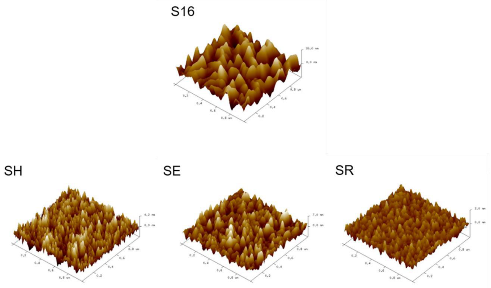
| S16 | 4 | 4 | 1 | 3 | 2 | 974.0 ± 8.0 | 12.2 ± 0.1 | 12.9 | 0.44 | 0.83 | 3.56 | 104.9 ± 3.3 | 7.1 ± 0.5 | 0.98 ± 0.07 | 5.5 ± 0.2 |
| SH | 4 | 1 | 3 | 2 | 3 | 945.0 ± 11.5 | 11.8 ± 0.1 | 6.7 | 0.36 | 1.46 | 3.57 | 100.1 ± 2.3 | 1.0 ± 0.1 | −0.89 ± 0.05 | 9.3 ± 0.2 |
| SE | 3 | 3 | 3 | 1 | 3 | 959.2 ± 4.4 | 12.0 ± 0.1 | 7.0 | 0.48 | 1.82 | 3.58 | 98.2 ± 2.1 | 1.6 ± 0.1 | 0.49 ± 0.04 | 6.8 ± 0.2 |
| SR | 1 | 1 | 4 | 2 | 2 | 1036.0 ± 24.5 | 13.0 ± 0.3 | 8.5 | 0.36 | 1.66 | 3.58 | 105.1 ± 1.9 | 0.5 ± 0.1 | 0.12 ± 0.03 | 8.1 ± 0.1 |
| Specimen Number | Co (at.%) | Cr (at.%) | Fe (at.%) | Ni (at.%) | O (at.%) | Sum (at.%) |
|---|---|---|---|---|---|---|
| S1 | 26.5 | 25.2 | 23.1 | 22.9 | 2.3 | 100 |
| S2 | 26.5 | 26.3 | 23.1 | 22.3 | 1.9 | 100 |
| S3 | 26.7 | 25.1 | 22.7 | 23.1 | 2.4 | 100 |
| S4 | 25.9 | 25.8 | 23.1 | 22.7 | 2.5 | 100 |
| S5 | 26.1 | 25.8 | 23.5 | 22.6 | 2.1 | 100 |
| S6 | 26.0 | 25.6 | 23.3 | 22.4 | 2.7 | 100 |
| S7 | 26.7 | 25.3 | 22.9 | 22.6 | 2.5 | 100 |
| S8 | 26.9 | 25.4 | 22.9 | 22.9 | 2.0 | 100 |
| S9 | 26.9 | 25.3 | 22.8 | 22.9 | 2.1 | 100 |
| S10 | 26.4 | 26.0 | 23.0 | 22.4 | 2.3 | 100 |
| S11 | 27.4 | 25.0 | 23.3 | 22.1 | 2.1 | 100 |
| S12 | 27.5 | 25.3 | 22.6 | 22.2 | 2.4 | 100 |
| S13 | 26.9 | 24.8 | 22.4 | 22.8 | 3.0 | 100 |
| S14 | 27.6 | 25.7 | 22.8 | 22.3 | 1.7 | 100 |
| S15 | 27.1 | 25.7 | 22.6 | 22.3 | 2.2 | 100 |
| S16 | 28.4 | 26.0 | 22.6 | 20.9 | 2.2 | 100 |
| SH | 26.9 | 24.8 | 23.5 | 22.8 | 2.0 | 100 |
| SE | 27.3 | 24.8 | 23.2 | 22.9 | 1.8 | 100 |
| SR | 26.1 | 25.4 | 23.1 | 23.6 | 1.8 | 100 |
| Average | 26.8 ± 0.6 | 25.4 ± 0.4 | 23.0 ± 0.3 | 22.6 ± 0.5 | 2.2 ± 0.3 | 100 |
| Factor | SS | DOF | Contribution | MS | F |
|---|---|---|---|---|---|
| Substrate Bias | 0.81 | 3 | 39.55% | 0.27 | 3.54 |
| Substrate Temperature | 0.14 | (3) | (6.94%) | pooled | - |
| Working Pressure | 0.34 | (3) | (16.66%) | pooled | - |
| Rotation Speed | 0.20 | (3) | (9.96%) | pooled | - |
| Frequency | 0.55 | 3 | 26.89% | 0.18 | 2.40 |
| Error | 0.68 | 9 | 33.56% | 0.08 | - |
| Total | 2.04 | 15 |
| Factor | SS | DOF | Contribution | MS | F |
|---|---|---|---|---|---|
| Substrate Bias | 168.59 | 3 | 29.96% | 56.20 | 5.52 |
| Substrate Temperature | 302.38 | 3 | 53.74% | 100.79 | 9.89 |
| Working Pressure | 28.24 | (3) | (5.02%) | pooled | - |
| Rotation Speed | 51.92 | (3) | (9.23%) | pooled | - |
| Frequency | 11.52 | (3) | (2.05%) | pooled | - |
| Error | 91.68 | - | 16.29% | 10.19 | - |
| Total | 562.65 | 15 |
| Factor | SS | DOF | Contribution | MS | F |
|---|---|---|---|---|---|
| Substrate Bias | 0.29 | (3) | (2.30%) | pooled | - |
| Substrate Temperature | 6.67 | 3 | 52.15% | 2.22 | 12.96 |
| Working Pressure | 4.57 | 3 | 35.78% | 1.52 | 8.89 |
| Rotation Speed | 0.95 | (3) | (7.45%) | pooled | - |
| Frequency | 0.30 | (3) | (2.32%) | pooled | - |
| Error | 1.54 | 9 | 12.07% | 0.17 | - |
| Total | 12.79 | 15 |
Publisher’s Note: MDPI stays neutral with regard to jurisdictional claims in published maps and institutional affiliations. |
© 2022 by the authors. Licensee MDPI, Basel, Switzerland. This article is an open access article distributed under the terms and conditions of the Creative Commons Attribution (CC BY) license (https://creativecommons.org/licenses/by/4.0/).
Share and Cite
Zhong, J.-Y.; Wang, J.-J.; Ouyang, F.-Y. Optimization of Sputtering Process for Medium Entropy Alloy Nanotwinned CoCrFeNi Thin Films by Taguchi Method. Materials 2022, 15, 8238. https://doi.org/10.3390/ma15228238
Zhong J-Y, Wang J-J, Ouyang F-Y. Optimization of Sputtering Process for Medium Entropy Alloy Nanotwinned CoCrFeNi Thin Films by Taguchi Method. Materials. 2022; 15(22):8238. https://doi.org/10.3390/ma15228238
Chicago/Turabian StyleZhong, Jing-Yi, Jian-Jie Wang, and Fan-Yi Ouyang. 2022. "Optimization of Sputtering Process for Medium Entropy Alloy Nanotwinned CoCrFeNi Thin Films by Taguchi Method" Materials 15, no. 22: 8238. https://doi.org/10.3390/ma15228238
APA StyleZhong, J.-Y., Wang, J.-J., & Ouyang, F.-Y. (2022). Optimization of Sputtering Process for Medium Entropy Alloy Nanotwinned CoCrFeNi Thin Films by Taguchi Method. Materials, 15(22), 8238. https://doi.org/10.3390/ma15228238