1. Introduction
The homoepitaxial and heteroepitaxial growth of diamonds have been explored and optimized for different technological applications [
1]. In recent years, many advances have been made to enable the growth of high-quality homoepitaxial single-crystal diamond (SCD) films for the development of optical and optoelectronic devices, as SCD films are excellent transparent semiconductor materials that also exhibit exceptional electrical, thermal, chemical and mechanical properties [
2]. This has stimulated the research and development of diamond-based semiconductor devices with potential use in harsh environments such as high temperatures (>400 °C), high voltages (>10 kV) and extreme radiation conditions [
2]. However, the wide adoption of SCD in microelectronics and optoelectronics has still been limited by the size of available high-quality natural and synthetic HPHT diamond crystals [
3].
Different CVD growth techniques and conditions have been investigated and used to produce high-quality SCD films [
4,
5,
6,
7,
8,
9]. The effects of temperature, pressure and holder geometry on the homoepitaxial SCD growth by microwave-assisted chemical vapor deposition were discussed by Widmann et al. [
4]. Bushuev et al. showed that an SCD growth rate of up to 82 μm/h can be achieved by optimizing the substrate temperature [
8]. More recently, Vikharev et al. reported the growth of high-quality (100)-oriented SCD with a growth rate of 6−8 μm/h [
5]. In another recent article, Zhang et al. reported the effect of CH
4/H
2 flow rates varied from 6% to 6.2%, 6.4%, 7% and 8% on the growth of SCDs. It was observed that under the optimized condition of 6.4% methane concentration, the growth rate was 3 µm/h [
9]. The influence of methane concentration on the growth rate and structure of single-crystal CVD diamond has also been discussed in other previous studies [
10,
11,
12]. Achard et al. investigated the evolution of the growth rate varying the CH
4 concentration from 2% to 7% [
11], whereas Bogdan et al. used from 6% to 15% [
12].
Although progress has been made, an improved understanding of high-quality CVD SCD film large area growth with suitable thickness is still required to design and fabricate diamond-based semiconductor devices with high performance and good reliability. In this paper, we exploit the MWPACVD technique to obtain a very high growth rate of SCD films by varying the methane concentration from 6% to 12%. A very high SCD film growth rate of up to 27 µm/h was obtained. In addition, the structural quality of the films is discussed in detail.
2. Materials and Methods
The experiments reported here have been performed on <100> oriented yellow HPHT type Ib seed substrates (3 × 3 × 1.1 mm3) from the Chenguang Machinery & Equipment Co., Ltd. (Changsha, China). The full width at half maximum (FWHM) of the Raman diamond spectral peak and HRXRD rocking curve were 4.8–5.3 cm−1 (1333.2 cm−1) and 0.012°, respectively. By optical profilometry in VSI measurement mode., all selected substrates presented an arithmetic average roughness (Ra) lower than 7.0 nm, for an analyzed area of 300 × 230 μm2. The substrates were first cleaned in effervescent aqua regia acid solution at 100 °C for 60 min, followed by washing with acetone, isopropyl alcohol and deionized water in an ultrasonic bath for 10 min and then dried with a heat gun. This was done with the aim of removing traces of metallic elements, graphite and other organic contaminants. Each sample was loaded individually on a modified substrate carrier into the chamber, which was then evacuated with a diffuser pump to 10−5 Torr for 30 min.
A feed gas mixture of hydrogen and methane gases with purity levels of 99.999% and 99.99%, respectively, was used for all experiments. The methane (CH
4) concentration in the gas phase was varied from 6% to 12% in balanced hydrogen. Prior to film growth, the substrates were etched in a H
2 plasma for 40 min at 1040 °C. SCD films were grown in a cylindrical cavity MWPACVD reactor designed to operate with a 6 kW and 2.45 GHz microwave generation system, specifically optimized for this experiment with the parameters given below. All samples were exposed to the same growth environment with 3.6 kW microwave power, a pressure of 150 Torr and a temperature of 1060 ± 10 °C for a total growth time of 10 h. The methane concentration was 6%, 8%, 10% and 12% diluted in H
2 at a total flow of 200 sccm, as shown in
Table 1. This CH
4 concentration range was chosen based on the conclusions of previous studies on CVD single-diamond growth without nitrogen addition [
9,
13]. Temperature control was performed by micrometrical positioning of a copper heat exchanger with a servomotor and monitored with a high resolution (0.1 °C) two-color infrared pyrometer (MERGENTHALER LASCON 101 LPC-03, Neu-Ulm, Germany).
After growth, samples had their bottom faces cleaned by simple grinding with a polishing cloth and 3 µm diamond paste. The samples were then boiled again in aqua regia solution at 100 °C for 60 min, rinsed in deionized water, and cleaned in an ultrasonic bath for 10 min with acetone, followed by further ultrasonic cleaning in isopropanol for 10 min. The SCD films’ structural quality was investigated by: (i) Raman and photoluminescence (PL) spectroscopy using a Horiba Labram HR evolution spectrometer (Kyoto, Japan) applying a 514.5 nm wavelength Nd:YAG laser source at room temperature, (ii) digital camera images using a Digilab DI-106T stereoscope (São Paulo, Brazil), (iii) SEM micrography using Tescan VEGA3 and MIRA3 electron microscopes (Brno, The Czech Republic) to analyze surface morphology, (iv) optical profilometry using a Veeco WYKO NT1100 profilometer, and (v) high-resolution X-ray diffractometry (HRXRD) using a PANalytical X’Pert setup (Malvern, UK) equipped with a four-crystal Ge(220) monochromator placed after the copper X-ray tube, which leads to Cu Kα1 radiation (λ = 1.5406 Å) for the incident beam, and an open gas proportional detector with an acceptance angle of 1° for the diffracted beam.
3. Results
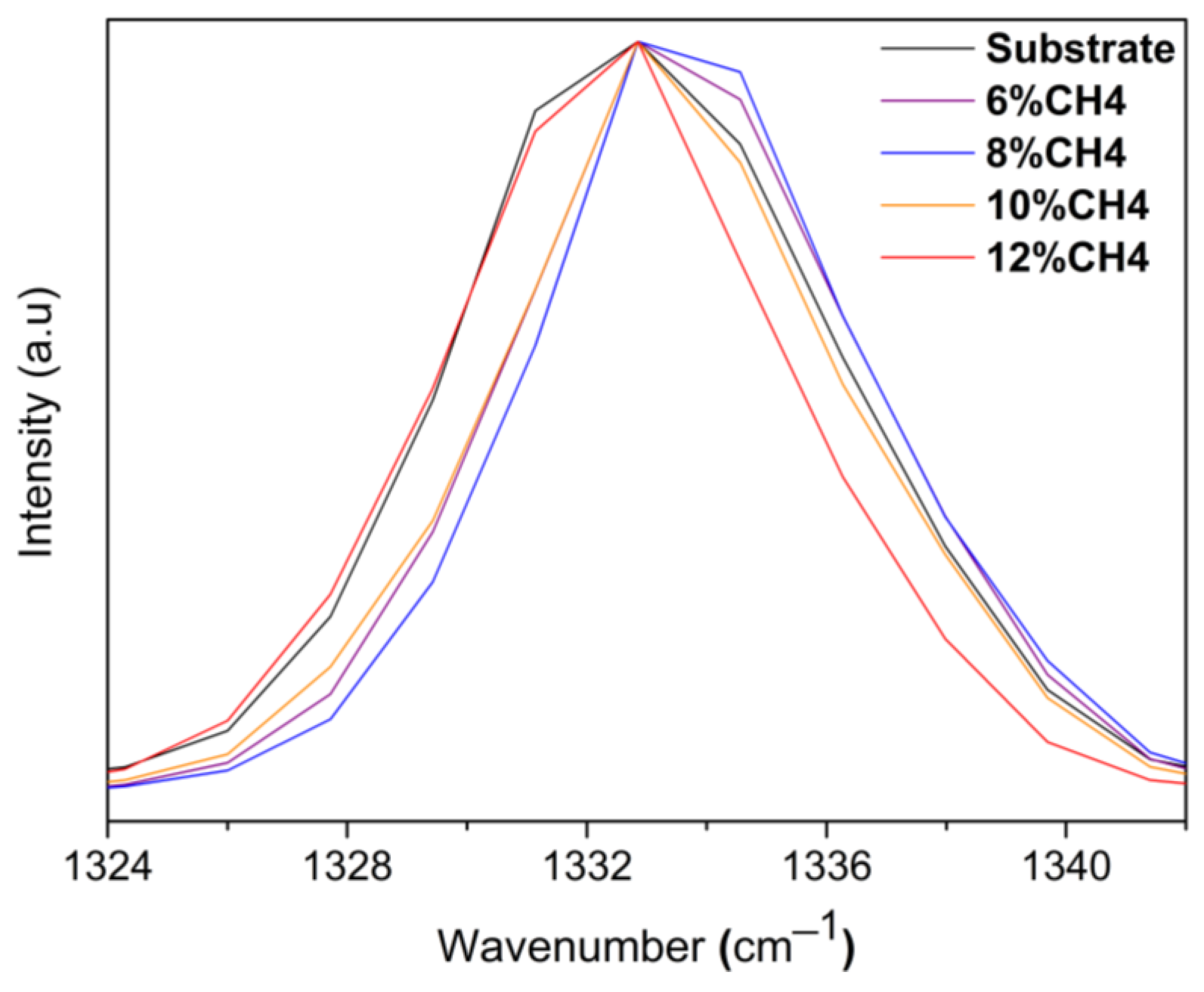
3.1. Raman Analysis
The whole surface of the grown SCD films was analyzed by Raman spectroscopy to evaluate the homogeneity of structural quality. A value of FWHM of the characteristic diamond peak centered at 1332 cm
−1 was used. The lowest FWHM obtained for each grown sample was compiled for comparison (
Figure 1).
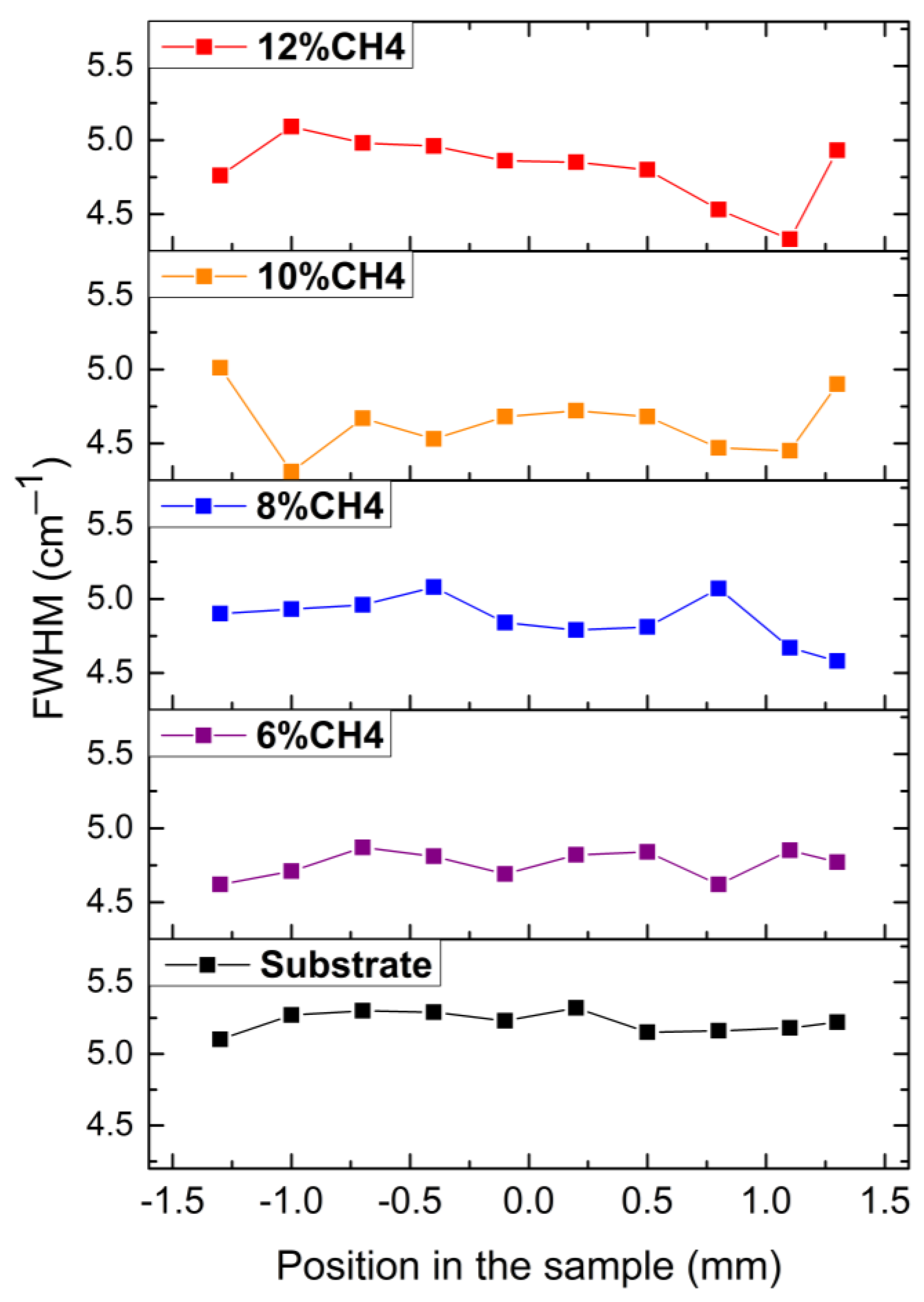
The structural quality of the substrates was also evaluated by this methodology. This allowed us to create an initial standard to compare each sample result separately. In
Figure 2, values for the FWHM of the Raman Scattering diamond peak are summarized for each sample in relation to the position of the measurement at the sample surface.
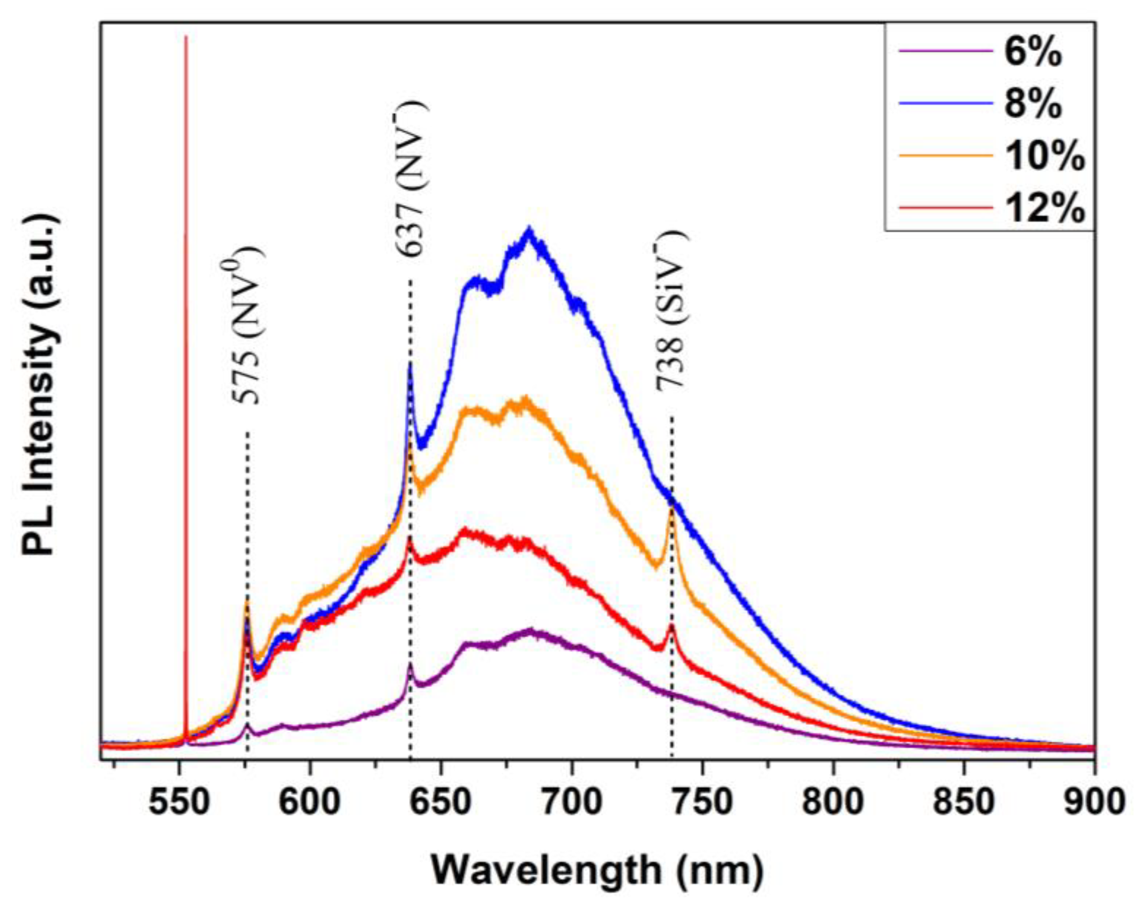
3.2. PL Measurements
It is also possible to identify some features of the grown film when a PL spectrum is measured at the sample and compared to the substrate, as shown in
Figure 3.
Luminescence is present at discrete wavelengths accompanied by an almost linear increase in the spectrum baseline, which is a common feature in polycrystalline CVD diamonds. This phenomenon is related to the incorporation of non-diamond phases in the grown material, which may be influenced by the growth rate of the films. If the crystal grows too quickly, some hydrocarbon radicals from CH4 dissociation in the surface do not properly react with the exposed binding sites and are incorporated with different hybridization to the lattice. Therefore, a delicate balance between diamond growth rate, and CH4 and nitrogen concentration is critical to achieving high quality, color grade and application properties.
3.3. Growth Rate
As
Figure 4 shows, there is a significant increase in the thickness of grown films as the CH
4 concentration is increased. All samples were grown for the same time of 10 h. The first sample grown at 6% CH
4 concentration achieved a thickness of around 165 µm and the thickness of the last one grown at 12% CH
4 concentration reached around 270 µm. This difference in deposited material could have positively impacted the measured FWHM. In addition, accelerated growth may cause luminescence increases, once more non-diamond particles are incorporated into the film, whereas a slight improvement in diamond quality is also perceivable with the increase in CH
4 concentration.
The growth rate is also impacted by nitrogen addition and its effects have been extensively studied by many different authors [
14,
15]. In our experiments, no intentional nitrogen was added to the process, but it was present in feed gases as a contaminant, and also introduced through leakages in the vacuum system. The total amount of nitrogen added to the process was estimated using equation 1 for the amount of nitrogen entering the chamber from vacuum leakage:
where [
N2] is the amount of nitrogen entering the chamber through vacuum leakages in ppm, Δ
P is the variation of pressure per minute in Torr,
Vc is the chamber volume in cm
3,
ṁ is the total gas flow in sccm, and 0.78 is the ratio of nitrogen content in air. By this method, we calculated that the amount of nitrogen from leakage was 46.6 ppm. For the nitrogen coming from gas impurities, we applied Equation (2) based on information provided by technical analysis reports from the gases’ manufacturers:
where [
N2] is the total amount of nitrogen in ppm entering the process from feed gases, [
N2/
H2] and [
N2/
CH4] are the concentrations of nitrogen in ppm in the hydrogen and methane gases respectively, and
ṁH2 and
ṁCH4 are the total flow of hydrogen and methane in sccm. The results considering the impurity levels of the gases we used are summarized in
Table 2 [
16].
In a recent article, Wu et al. discussed the influence of nitrogen addition on the defects, morphologies and growth rate of single-crystal CVD diamond films produced by microwave plasma chemical vapor deposition (MPCVD) [
17]. The CH
4/H
2 ratio was set at 4% with a hydrogen flow rate of 200 sccm. The nitrogen concentration in the CH
4/H
2/N
2 gas mixtures was varied from 0–9524 ppm. The highest growth rate achieved was 23 µm/h at a N
2 concentration of 5261 ppm, whereas in our study without intentional nitrogen addition we obtained a growth rate of 27 µm/h. Furthermore, according to their conclusions, as the nitrogen concentration increases, the structure and content of the defects evolve as well, with the domination of point defects, probably leading to lattice deformation in the as-grown diamond films in addition to eventually leading to variations in the surface roughness and uniformity of the diamond films.
3.4. Surface Morphology
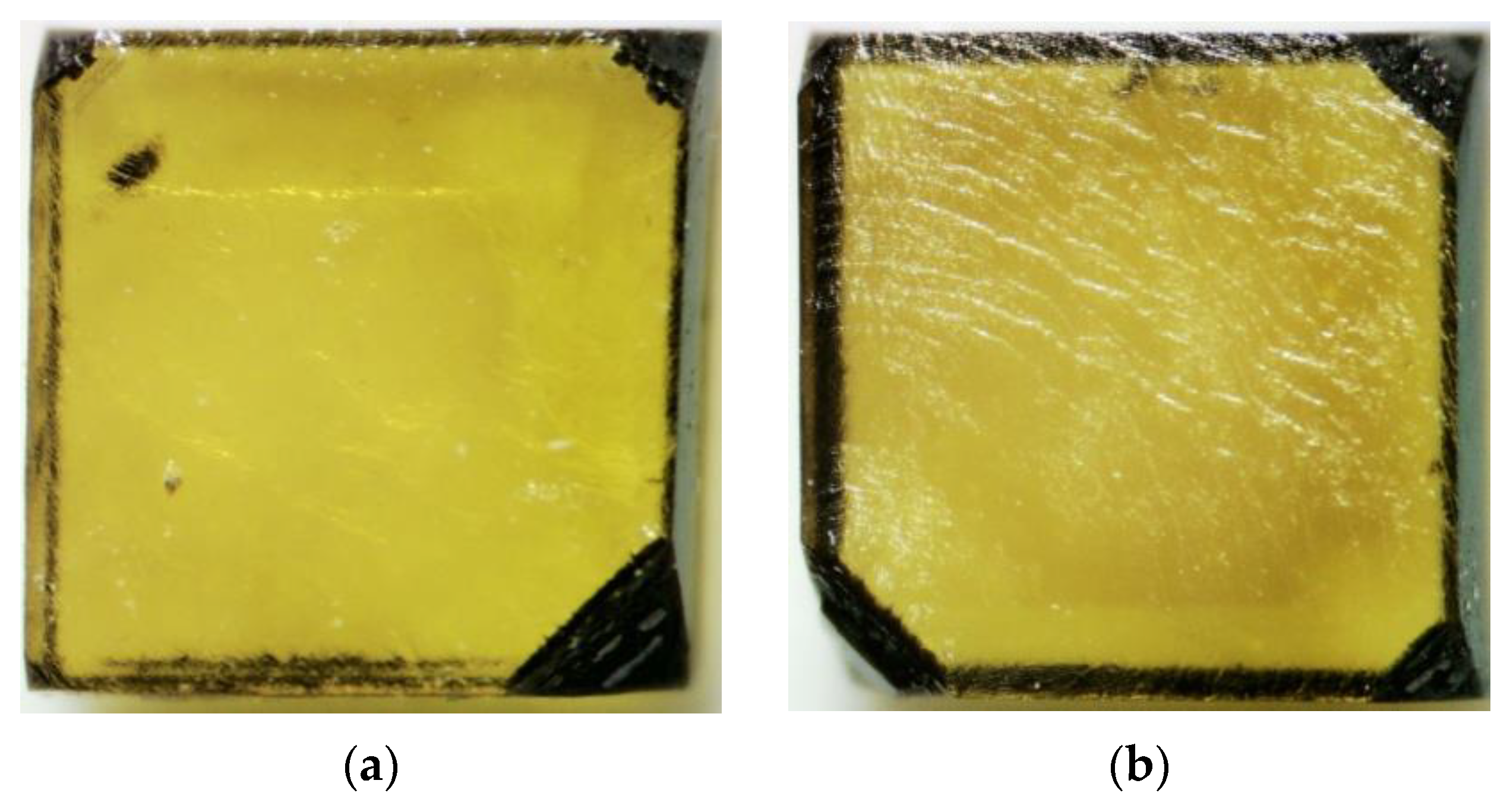
Images obtained with optical microscopy are shown in
Figure 5. It is possible to observe that our grown layers are nearly colorless over the yellow, type Ib HPHT seed substrate, despite the considerable amount of nitrogen incorporated in the films. For the sample grown at a CH
4 concentration of 8%, shown in
Figure 5b, some of the striations from step-growth are visible, this feature is present in all samples and will be further examined in the discussion of the results of the SEM and profilometry analyses below.
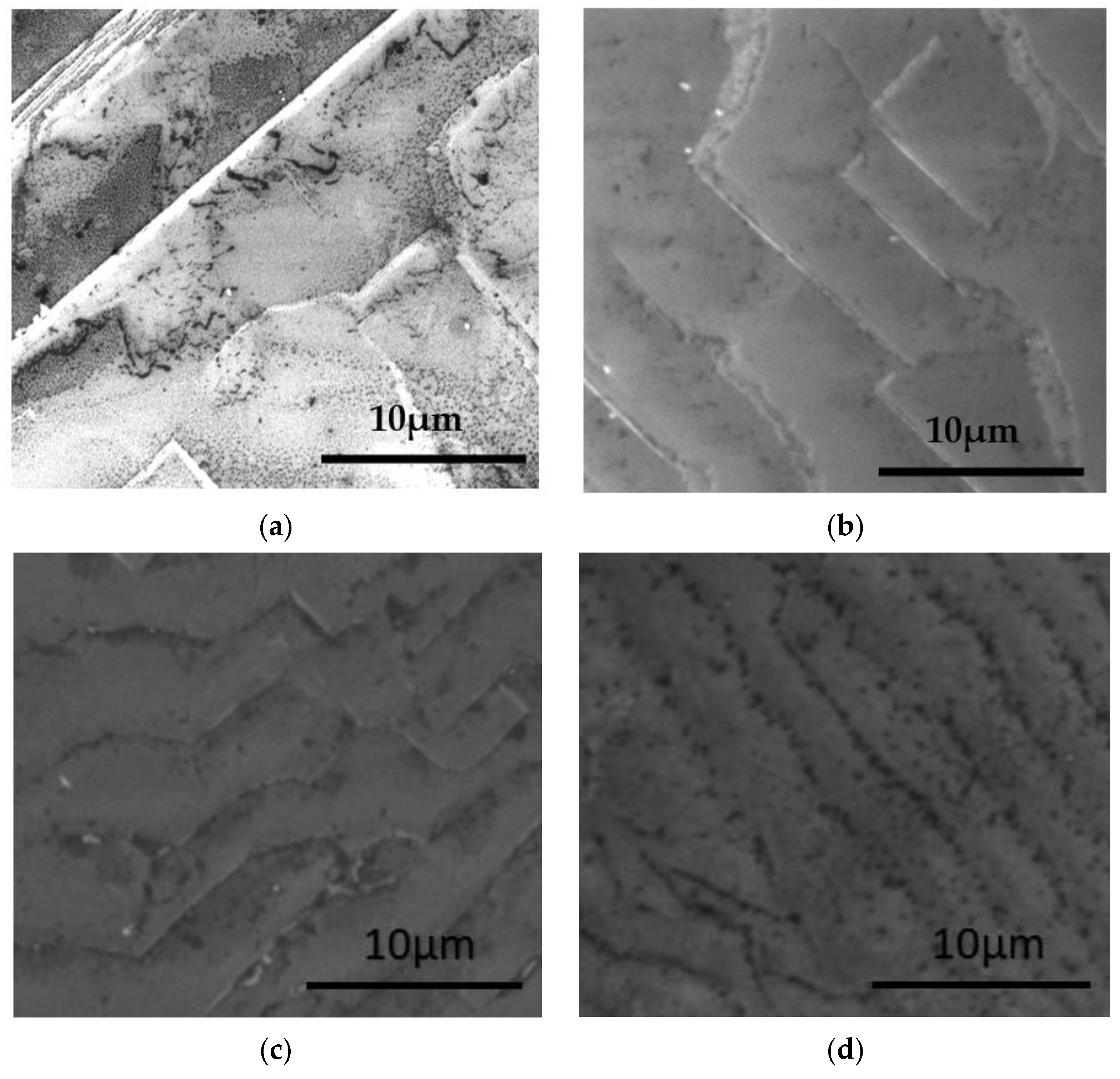
SEM analyses were employed to identify in detail some features of the striations formed by the step-growth regime of the films. It is noticeable in the obtained micrographs (
Figure 6), that as well as the formation of steps, some square-shaped features are present (
Figure 6a–c). This is related to the growth of the steps in a screw pattern centered at dislocations present in the crystal [
18].
In
Figure 7, we show results for profilometry conducted to better understand how growth steps can influence the morphology of the top surface. We found that surface roughness can be significantly affected by CH
4 concentration, with the length of the growth steps being inversely proportional to the increase in CH
4 concentration. This caused the roughness (Ra) to fall from 629.13 nm for the sample grown with 6% CH
4 to 171.59 nm for the sample grown with 12% CH
4. Values for Ra of all samples are summarized in
Table 3.
3.5. High-Resolution X-ray Diffraction Analysis
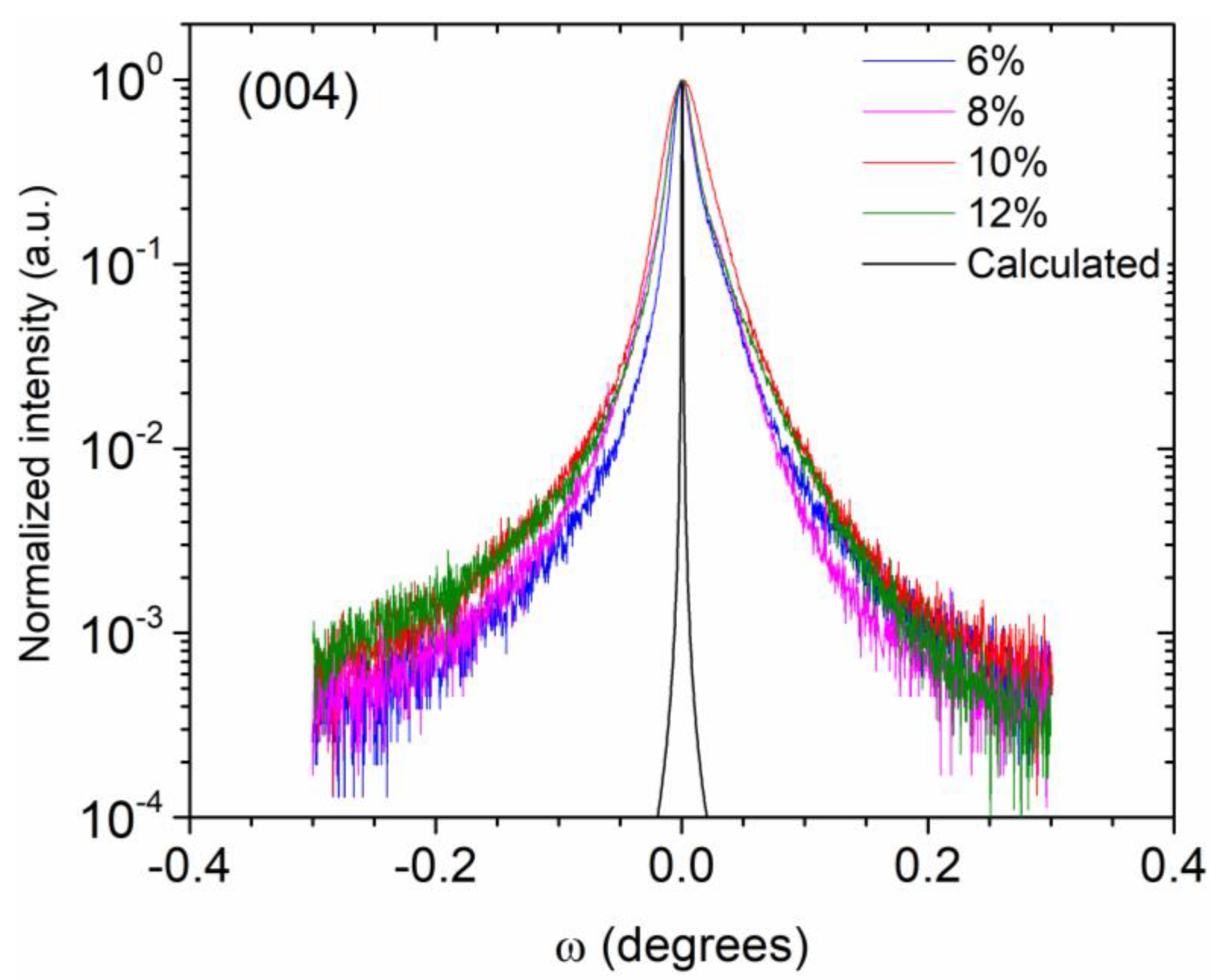
X-ray diffraction curves (ω scans) were measured around the (004) Bragg peak for all samples.
Figure 8 shows these curves for the samples with the different methane concentrations investigated here. To correct the offset in the ω axis, all curves were shifted to the central position to allow comparison. The X-ray curves are very similar and independent of the CH
4 concentration. Their FWHM values, displayed in
Table 4, range from 0.014° to 0.028° and are equivalent to values published in the literature [
19,
20]. It is important to observe that the attenuation length of the X-ray incident beam in diamond crystals calculated for λ = 1.5406 Å is 570 μm, which is three times the thickness of the grown diamond films. Therefore, the measured X-ray curves are a convolution of the diffracted beam coming from both the diamond film and the diamond substrate. This result demonstrates that the diamond films grown in this work present a crystal quality comparable to the commercial HPHT substrate. The (004) diamond Bragg peak was calculated by the dynamical theory of X-ray diffraction using the Takagi–Taupin equations [
21]. For comparison, the calculated curve is also included in
Figure 8, and its linewidth is found to be 0.001
o, 20 times smaller than the measured linewidths.
4. Discussion
Nitrogen-vacancy defect complexes are identifiable in the spectra by the visible bands centered at 575 nm and 637 nm in the PL spectra, for NV
0 and NV
-, respectively. At the same time, the substrate did not present the same features, even though it is a type Ib substrate that also has nitrogen incorporated in the grown diamond. This difference in the incorporation of nitrogen, as well as its concentration, inside the diamond lattice, plays a key role in many properties of the film, especially in its color. CVD-grown diamond usually presents a brown hue, which can become darker with higher nitrogen concentrations in the gas phase. This color is attributed to the color centers of the vacancies. HPHT-grown diamond has nitrogen as single substitutional atoms in the lattice, and this kind of incorporation leads to the characteristic yellow color of these synthetic stones [
22].
An additional band that is present in some of our samples is the 737 nm SiV center. This is a commonly-observed band for CVD diamond, as microwave plasma reactors usually employ solutions to handle the magnetic and electric fields involving quartz domes, tubes, or windows. Silicon from these components is removed by plasma etching or heating and can incorporate into the diamond lattice as a substitutional atom, creating neighboring vacancies in the structure. The emission from this center is related to the nitrogen content in the grown diamond. Tallaire et al. observed that higher levels of nitrogen doping increase the intensity of this band [
15].
Our samples also presented significant lateral growth of the same order as the top surface growth. This is a common feature in MWPACVD diamond homoepitaxial layers, also described by other authors [
23,
24]. The lateral growth can be observed by the black line at the borders of the samples. The thickness of these borders is roughly the film thickness itself.
In a general manner, this growth pattern is observed for single and polycrystalline diamonds oriented in the [001] direction [
18,
25]. Tallaire et al. also reported the contribution of nitrogen content to the formation of growth steps and observed a surface free of this surface feature for a film grown with no added nitrogen [
15]. However, it is not clear if the addition of nitrogen per se causes a reduction of the step size or if this could only be related to the growth rate. A more detailed study is needed to elucidate the phenomena involved in their formation.
5. Conclusions
Homoepitaxial single crystal diamond (SCD) films were produced using the MWPACVD process with a high deposition rate from 16.5 to 27 µm/h by varying the methane concentration in the reactor from 6% to 12%. The thickness of the SCD films was correlated with their structure, morphology and appearance. The results obtained demonstrate the good structural quality of the grown SCD films. This study represents an advance in attempts to optimize the growth of high-quality SCD films for different applications. It was possible to evaluate the influence of the concentration of CH4 by scanning electron microscopy, which was confirmed by optical profilometry, with a decrease in the surface roughness from Ra = 624.13 nm with 6% CH4 to Ra = 171.59 nm with 12% CH4. Thus, Ra was inversely proportional to the percentage of CH4 in the gas mixture. Therefore, the smoothest step growth surface was obtained with 12% CH4; which was, however, impacted by the higher unintentional incorporation of nitrogen into the film from the CH4 gas. In terms of structural quality, 8% CH4 was the best condition with an average FWHM of 4.6 cm−1. At the same time, in terms of the crystalline quality of the grown SCD, the X-ray curves were very similar and the FWHM varied between 0.014–0.018°, except for 10% CH4, which was 0.028°; and the PL measurements indicated that this concentration of CH4 favored the formation of NV defects. These results showed that diamond films grown at 6–12% CH4 had good crystalline quality. Overall, this study contributes toward the understanding of single CVD diamond growth and their morphology and structure.
Author Contributions
Conceptualization and methodology, J.V., J.S.G. and V.J.T.-A.; formal analysis, J.V., J.S.G., M.A.F., E.J.C. and V.J.T.-A.; investigation, J.V., J.S.G., E.J.C. and V.J.T.-A.; resources, E.J.C. and V.J.T.-A.; writing—original draft preparation, J.V., J.S.G. and M.A.F.; writing—review and editing, J.V., J.S.G., M.A.F., E.J.C. and V.J.T.-A.; project administration, E.J.C. and V.J.T.-A.; funding acquisition, M.A.F., E.J.C. and V.J.T.-A. All authors have read and agreed to the published version of the manuscript.
Funding
This research was funded by São Paulo Research Foundation: 2014/18139-8, 2015/158571-1, and 2019/18572-7; CAPES; CNPq.
Institutional Review Board Statement
Not applicable.
Informed Consent Statement
Not applicable.
Data Availability Statement
Not applicable.
Acknowledgments
The authors are grateful to Eduardo Abramof for his valuable discussions on x-rays diffraction measurements and calculations.
Conflicts of Interest
The authors declare no conflict of interest.
References
- Liu, H.; Dandy, D.S. Diamond Epitaxy, Oriented Growth, and Morphology Evolution. In Diamond Chemical Vapor Deposition; Elsevier: Amsterdam, The Netherlands, 1995; pp. 79–91. [Google Scholar]
- Yang, J.; Huang, W.; Chow, T.P.; Butler, J.E. Free-standing Diamond Single Crystal Film for Electronics Applications. MRS Online Proc. Libr. 2005, 905. [Google Scholar] [CrossRef]
- Hemley, R.J.; Chen, Y.-C.; Yan, C.-S. Growing Diamond Crystals by Chemical Vapor Deposition. Elements 2005, 1, 105–108. [Google Scholar] [CrossRef]
- Widmann, C.; Müller-Sebert, W.; Lang, N.; Nebel, C. Homoepitaxial growth of single crystalline CVD-diamond. Diam. Relat. Mater. 2016, 64, 1–7. [Google Scholar] [CrossRef]
- Vikharev, A.L.; Lobaev, M.A.; Gorbachev, A.M.; Radishev, D.B.; Isaev, V.A.; Bogdanov, S.A. Investigation of homoepitaxial growth by microwave plasma CVD providing high growth rate and high quality of diamond simultaneously. Mater. Today Commun. 2020, 22, 100816. [Google Scholar] [CrossRef]
- Arnault, J.C.; Saada, S.; Ralchenko, V. Chemical Vapor Deposition Single-Crystal Diamond: A Review. Phys. Status Solidi (RRL)–Rapid Res. Lett. 2022, 16, 2100354. [Google Scholar] [CrossRef]
- Cao, W.; Ma, Z.; Gao, D.; Fu, Q.; Zhao, H. Homoepitaxial lateral growth of single-crystal diamond with eliminating PCD rim and enlarging surface area. Vacuum 2022, 197, 110820. [Google Scholar] [CrossRef]
- Bushuev, E.; Yurov, V.; Bolshakov, A.; Ralchenko, V.; Khomich, A.; Antonova, I.; Ashkinazi, E.; Shershulin, V.; Pashinin, V.; Konov, V. Express in situ measurement of epitaxial CVD diamond film growth kinetics. Diam. Relat. Mater. 2017, 72, 61–70. [Google Scholar] [CrossRef]
- Zhang, P.; Chen, W.; Zhang, L.; He, S.; Wang, H.; Yan, S.; Ma, W.; Guo, C.; Wang, Y. Evolution of High-Quality Homoepitaxial CVD Diamond Films Induced by Methane Concentration. Coatings 2021, 11, 888. [Google Scholar] [CrossRef]
- Silva, F.; Achard, J.; Bonnin, X.; Brinza, O.; Michau, A.; Secroun, A.; De Corte, K.; Felton, S.; Newton, M.; Gicquel, A. Single crystal CVD diamond growth strategy by the use of a 3D geometrical model: Growth on (113) oriented substrates. Diam. Relat. Mater. 2008, 17, 1067–1075. [Google Scholar] [CrossRef]
- Achard, J.; Silva, F.; Tallaire, A.; Bonnin, X.; Lombardi, G.; Hassouni, K.; Gicquel, A. High quality MPACVD diamond single crystal growth: High microwave power density regime. J. Phys. D Appl. Phys. 2007, 40, 6175–6188. [Google Scholar] [CrossRef]
- Bogdan, G.; Nesládek, M.; D’Haen, J.; Haenen, K.; D’Olieslaeger, M. Freestanding (100) homoepitaxial CVD diamond. Diam. Relat. Mater. 2006, 15, 508–512. [Google Scholar] [CrossRef]
- Bolshakov, A.; Ralchenko, V.; Yurov, V.; Popovich, A.; Antonova, I.; Khomich, A.; Ashkinazi, E.; Ryzhkov, S.; Vlasov, A. High-rate growth of single crystal diamond in microwave plasma in CH4/H2 and CH4/H2/Ar gas mixtures in presence of intensive soot formation. Diam. Relat. Mater. 2016, 62, 49–57. [Google Scholar] [CrossRef]
- Zaitsev, A.; Moe, K.; Wang, W. Defect transformations in nitrogen-doped CVD diamond during irradiation and annealing. Diam. Relat. Mater. 2018, 88, 237–255. [Google Scholar] [CrossRef]
- Tallaire, A.; Collins, A.; Charles, D.; Achard, J.; Sussmann, R.; Gicquel, A.; Newton, M.; Edmonds, A.; Cruddace, R. Characterisation of high-quality thick single-crystal diamond grown by CVD with a low nitrogen addition. Diam. Relat. Mater. 2006, 15, 1700–1707. [Google Scholar] [CrossRef]
- Nad, S. Growth and Characterization of Large, High Quality Single Crystal Diamond Substrates via Microwave Plasma Assisted Chemical Vapor Deposition. Ph.D. Thesis, Michigan State University, East Lansing, MI, USA, 2016. [Google Scholar] [CrossRef]
- Wu, G.; Wang, Q.; Wu, Y.; Sun, X.; Liao, J.; Pan, J.; Chen, M.; Kasu, M.; Liu, S. Evolution of defects, morphologies and fundamental growth characteristics of CVD diamond films induced by nitrogen addition. Mater. Today Commun. 2020, 25, 101504. [Google Scholar] [CrossRef]
- Schwarz, S.; Rottmair, C.; Hirmke, J.; Rosiwal, S.; Singer, R. CVD-diamond single-crystal growth. J. Cryst. Growth 2004, 271, 425–434. [Google Scholar] [CrossRef]
- Yamamoto, Y.; Imai, T.; Tanabe, K.; Tsuno, T.; Kumazawa, Y.; Fujimori, N. The measurement of thermal properties of diamond. Diam. Relat. Mater. 1997, 6, 1057–1061. [Google Scholar] [CrossRef]
- Wang, X.; Duan, P.; Cao, Z.; Liu, C.; Peng, Y.; Hu, X. Homoepitaxy Growth of Single Crystal Diamond under 300 torr Pressure in the MPCVD System. Materials 2019, 12, 395. [Google Scholar] [CrossRef]
- Bartels, W.J.; Hornstra, J.; Lobeek, D.J.W. X-ray diffraction of multilayers and superlattices. Acta Crystallogr. Sect. A Found. Crystallogr. 1986, 42, 539–545. [Google Scholar] [CrossRef]
- Zheng, Y.; Li, C.; Liu, J.; Wei, J.; Ye, H. Diamond with nitrogen: States, control, and applications. Funct. Diam. 2021, 1, 63–82. [Google Scholar] [CrossRef]
- Wu, G.; Chen, M.-H.; Liao, J. The influence of recess depth and crystallographic orientation of seed sides on homoepitaxial growth of CVD single crystal diamonds. Diam. Relat. Mater. 2016, 65, 144–151. [Google Scholar] [CrossRef]
- Nad, S.; Gu, Y.; Asmussen, J. Growth strategies for large and high quality single crystal diamond substrates. Diam. Relat. Mater. 2015, 60, 26–34. [Google Scholar] [CrossRef]
- Martineau, P.; Gaukroger, M.; Khan, R.; Evans, D. Effect of steps on dislocations in CVD diamond grown on {001} substrates. Phys. Status Solidi C 2009, 6, 1953–1957. [Google Scholar] [CrossRef]
| Publisher’s Note: MDPI stays neutral with regard to jurisdictional claims in published maps and institutional affiliations. |
© 2022 by the authors. Licensee MDPI, Basel, Switzerland. This article is an open access article distributed under the terms and conditions of the Creative Commons Attribution (CC BY) license (https://creativecommons.org/licenses/by/4.0/).


 ,
, 


