1. Introduction
From industrial and economical points of view, metal sulfides have gained increasing importance due to their remarkable physical, electrical, and chemical characteristics. Pyrite (FeS
2), a polymorph of iron sulfide, is a good candidate for use in solar cells since it has excellent solid-state characteristics [
1]. The crystal structure of the mineral pyrite (β-FeS
2) is face-centered cubic and pyrite belongs to the
space group [
1]. The unit cell of pyrite contains four FeS
2 formula units [
2].The pyrite unit cell can be defined completely by
(the lattice constant) and
u (the S coefficient) that indicate the position of the Pyrite atom in the unit cell. In 1914, Bragg [
3] introduced the complete crystal structure of a pyrite unit cell for the first time, and now the well-accepted values of
and
are
and
, respectively [
4,
5]. Natural pyrites can be n-type or p-type (usually with arsenic), depending on the impurity type that they contain. The measured conductivity of natural pyrite is in the range of
[
6] and its measured band gap is about 0.9 eV [
2].
Nanocrystals of pyrite were successfully prepared two decades ago for the first time [
7]. Recently, large [
8] and small [
9] clusters of pyrite nanocrystals have been reported.
Nevertheless, so far, no efficient pyrite-based solar cells have been reported. It has been claimed that the main drawback is pyrite’s low illuminated open-circuit voltage (lower than 0.2 V) which is the consequence of its inherent low unilluminated short-circuit current, due to the existence of impurities and the high density of surface states of pyrite [
10].
So far, many methods have been used to synthesize pyrite [
11,
12,
13,
14,
15,
16,
17]. Some of the primary methods used to prepare single crystals of pyrite are chemical vapor transport (CVT) and high-temperature solution using tellurium as the solvent [
18].
According to Ostwald’s law, the production of pyrite by sulfurization of ferrous compounds starts from the production of iron sulfide (FeS), and as more sulfur diffuses the structure, iron disulfide (FeS
2) gradually forms. Since the diffusion coefficient of sulfur atoms in iron is high (
), FeS formation would occur immediately. However, the diffusion coefficient of sulfur in FeS is much lower than this, and thus, the formation of FeS
2 takes a longer time [
18].
To date, there have been many methods reported for producing pyrite thin films, including iron sulfurization, metal-organic chemical vapor deposition, and sintering of nanocrystals that have been prepared using the solvothermal method [
19,
20,
21].
A report conducted by Wan et al. [
22], in 2003, showed that the crystal structure, crystallization, stoichiometry, and more importantly, the preferential orientation of the crystal grains could affect the electrical and optical properties of pyrite thin films. Moreover, they demonstrated that it was the crystal grain size that specified the electrical properties, not the particle size. A year later, Ouertani et al. [
23] successfully prepared a pyrite thin film by sulfurization of a layer of amorphous iron oxide which had been deposited previously by spray pyrolysis.
Ennaoui and Tributsch [
24], in 1984, for the first time, showed the potential of crystalline pyrite to prepare a photoelectrochemical solar cell. Although the final cell they made could not reach over 1% conversion efficiency, they declared that the low raw material cost of pyrite and its inherent properties could make it a promising choice for use in the production of low-cost solar cells. They used pyrite as a solar cell’s synthesizer about a decade later and made a p-i-n structure solar cell [
18]. They sandwiched a very thin layer (10–20 nm thick) of pyrite between a p-type and an n-type semiconductor. The analysis showed that pyrite had a spectacular electron conduction feature through interfaces.
In 2009, a hybrid solar cell was made by using pyrite nanocrystals as small as 10 nm, which had been prepared by a chemical solution method [
9]. The conversion efficiency of this solar cell was 0.16%. Recently, cubic nanocrystals of pyrite, with 60–200 nm diameters, were used to prepare a Schottky-type photovoltaic solar cell with aluminum as the metallic contact [
25]. The current-voltage analysis showed no Schottky barrier. Steinhagen et al. [
26] used pyrite nanocrystals to make photovoltaic cells with four structures: Schottky, layered, depleted heterojunction, and hybrid. None of the structures showed a photovoltaic response.
Because of better catalytic activity, it has been claimed that the pyrite nano-rods have a higher short-circuit current in dye-synthesized solar cells as compared with pyrite layers [
12].
A chemical procedure reported by Vayssieres et al. [
27] has been recently used to grow nano-rod arrays of iron hematite (
) on any surface. The strategy involves controlling the thermodynamics and kinetics of interfaces during nucleation and growth which leads to good control of the size, shape, and structure of the final layer [
28]. The process is called aqueous chemical growth (ACG) [
29]. Precise control of the rate of heterogeneous nucleation and growth can result in one-dimensional growth and rod-like morphologies. Huang et al. [
12] used the same method with a further sulfurizing step to obtain pyrite nano-rod arrays.
In this paper, pyrite nano-rod arrays were prepared by developing a novel ACG process followed by calcination and sulfurization steps. The structure of the resulting layers, after each step, was characterized and the structural, electrical, and optical properties of the final layers were investigated to apply this semiconductor in photovoltaic devices. In addition, the combination of pyrite nano-rods and the Schottky-type solar cell is a novel way to prepare a solar cell. It is noteworthy to mention that, in this research, for the first time, no ionic salt was used for the ACG process. The ACG process electrolyte pH was merely controlled by HCl. The results pave the way for future low-cost solar cells.
2. Experimental Procedures
The precursors , pyrite, and HCl were purchased from Merck and used as received. Fluorine-doped tin oxide (FTO)-coated glass with 8 ohms electrical resistance was purchased from Solaronix. To prepare , the ACG method was established. The process started with 0.1 M iron chloride via mixing 5.4 g of in 200 mL distilled water, followed by a pH reduction to 1.5 by adding HCl.
A reflux system was prepared to run ACG at . FTO- and non-coated glass were used inside this system as two different substrates. In all samples, an orange layer was formed on both sides of the substrates, and an orange-colored sediment was deposited in the flask simultaneously. The substrates were gently removed from the flask and were quickly washed with water. Meanwhile, the sediments were dried in an oven at to obtain powder samples.
A muffle furnace was used for the calcination of the layered and powdered samples. Samples were tempered for 5 h at , and then they were cooled down to room temperature inside the furnace.
Then, the tempered samples were placed in a sealed quartz capsule with 1 g sulfur and were evacuated to 0.1 Torr, as depicted in
Figure 1. Afterward, these capsules were placed in the furnace at
for different times, and they were cooled to room temperature inside the furnace. Then, the samples were removed from capsules.
Table 1 summerizes sample coding system used in this research. The initial letter of the sample codes shows the sample type which means that glass, FTO-coated glass substrates, and powder sample codes start with G, F, and P, respectively. The number after this letter shows the process which was applied to the sample of that type. The second number shows the process variable (usually the processing time). G2 is the G17 sample after calcination. For more information about the process, please check the
Supplementary Materials section.
The structural, electrical, and optical properties of samples from different steps of the preparation were examined. Samples G12, G14, G17, G3, and F31 were analyzed using a field emission scanning electron microscope (FESEM). The electrical resistance of G3 was measured using a four-probe surface resistance scanner. X-ray diffraction analyses were carried out for P1, P2, and P3 powders and also for Samples F1, F2, F36, F31, F3.30, F3.10, G1, G2, and G3. The X-ray spectrum was emitted from with 40 kV voltage and 30 mA current. Samples G3, F36, F31, F3.30, and F3.10 were used for Raman analysis with a 10 MW laser with 785 nm wavelength to analyze the thin films. A UV-Vis analysis was also carried out for G3 with a light wavelength range of 190–1100 nm.
Furthermore, the performance of the prepared pyrite layers in a photovoltaic device was also examined. To examine the photovoltaic response, a 100 nm thick aluminum layer was deposited on the samples with FTO-coated glass substrate by using thermal evaporation. The current-voltage tests were carried out for final Schottky cells under airmass 1.5 with a illumination of a solar simulator.
3. Results and Discussion
After the ACG process, an orange semi-transparent layer was formed on the substrates. The FESEM images of Sample G17 show a large number of flower-like nano-rods which are formed on the substrate, as shown in
Figure 2. The mean diameter and length of the rods were 36 nm and 235 nm, respectively, measured from the FESEM images, and therefore, the mean aspect ratio of the nano-rods was 6.5.
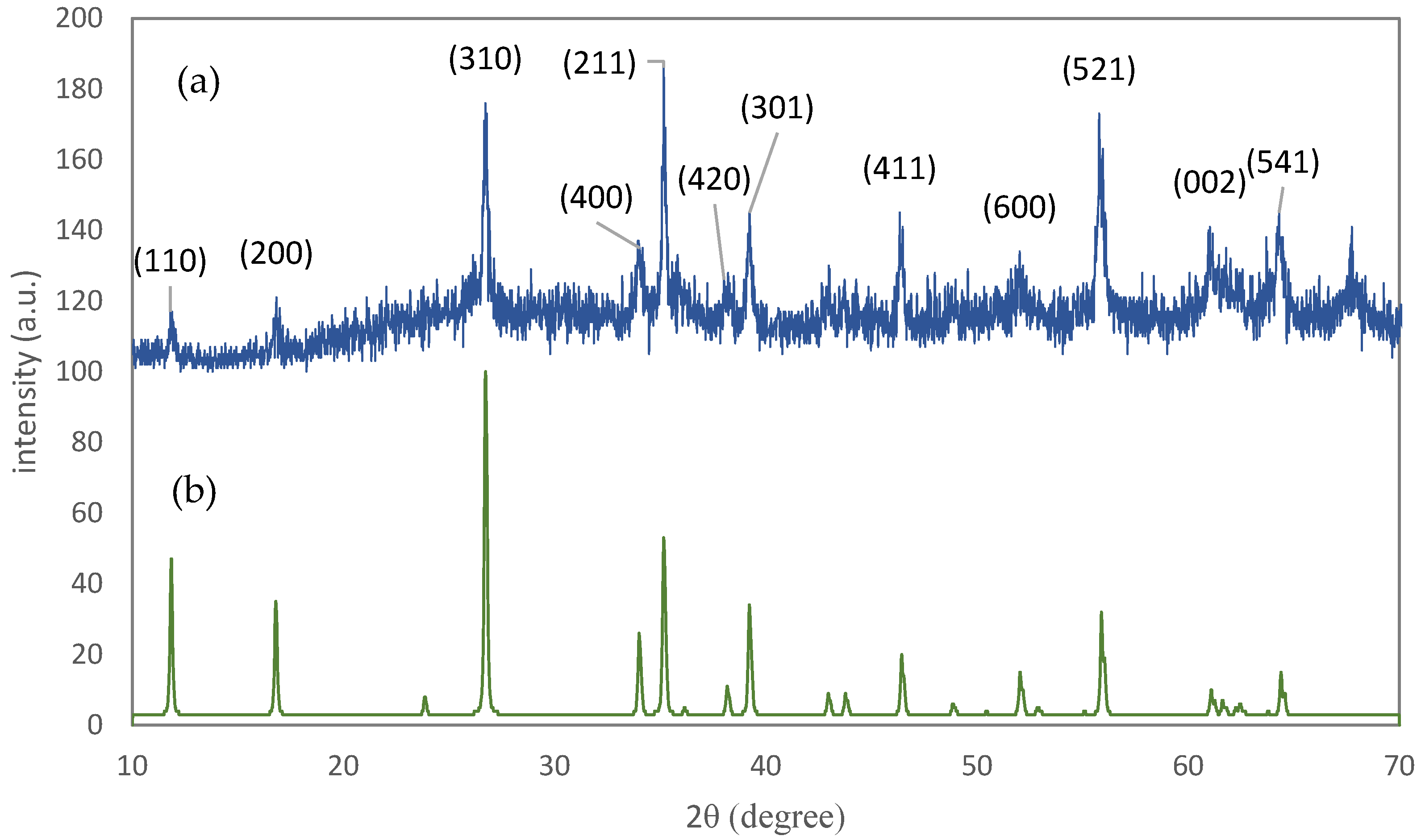
The XRD pattern of Sample F1 is shown in
Figure 3. The characteristic peaks of fluorine-doped tin oxide (FTO) and iron oxy-hydroxide (akaganéite) are visible in the pattern. This polymorph of FeOOH forms when a small amount of Cl is present in the crystal [
30] which, in our solution, was supplied by HCl. The high intensity of FTO peaks may be due to the high thickness of this layer in contrast with the iron oxy-hydroxide layer. The XRD pattern of the powder sample, Sample P1, was used to examine the crystallite size and preferential orientation of the nano-rods (
Figure 4). The crystallographic direction of each peak is labeled in
Figure 4 according to the reference pattern. The average crystallite size, which can be estimated from the empirical Scherrer equation, is
. By compareing this average crystallite size with the particle size measured from microscopic images, it can be said that each nano-rod contains six crystallographic grains, on average. The Lotgering factor,
, was also used to measure the preferential orientation of the nano-rods [
31]. The thin film’s orientation is totally parallel to the
orientation if
equals one, and is random if
equals zero. The calculated Lotgering factor was compared for the major crystallographic directions of Sample F1 in
Figure 5 by using the XRD patterns of the powder sample (P1) and the thin film sample (F1). The L factors for the 310 and 211 directions are higher than the other directions. The 310 direction could be omitted because of its overlap with the FTO peak. A higher L factor in some directions means that the akaganéite nano-rods are preferentially oriented. However, in the literature, it has been reported that the orientation is parallel to the c axis [
32,
33]. This contradiction may be due to the lack of use of ionic salts in the ACG process. Ionic salts may adhere to some crystal facets and slow down their growth rate.
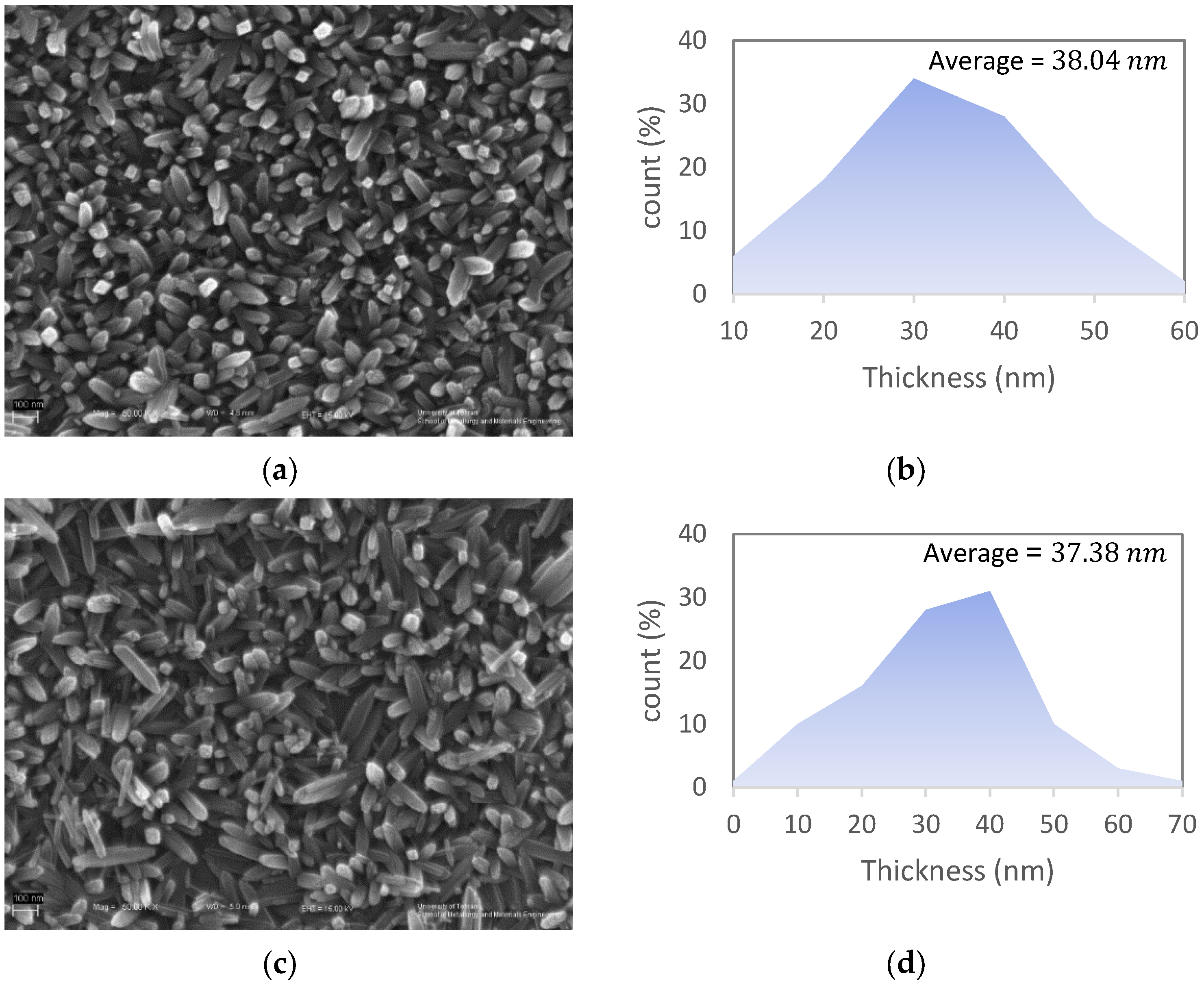
The effect of the ACG process time on morphology was also studied. Samples with 2 (G12), 4 (G14), and 7 (G17) hours of process time are compared in
Figure 6. It can be concluded that the ACG process time can affect the diameter distribution of the nano-rods, based on the demonstrated nano-rod thickness histograms in
Figure 6b–f. The skewness factor was calculated for different samples, as shown in
Figure 6g. The skewness factor is a measure of the asymmetry of a distribution. The sample with a 7 h ACG process time has a lower skewness factor than other samples, which means that the thickness distribution of the nano-rods in Sample G17 is more uniform.
The XRD pattern of the thin film with an FTO sublayer after calcination (F2) revealed two different phases: FTO and hematite (
), as shown in
Figure 7. During calcination, water molecules abandon the akaganéite phase and the crystal structure transforms from tetragonal (I4/m) to trigonal (R
c), and finally the hematite phase starts to form. The hematite crystallite size, according to the Scherrer equation, is
, which suggests a little grain growth during calcination. The calculated Lotgering factors for different crystal directions of the thin film sample (F2), according to the XRD pattern of the powder sample (P2), are shown in
Figure 8. The preferential crystallographic direction of hematite nano-rods is [012].
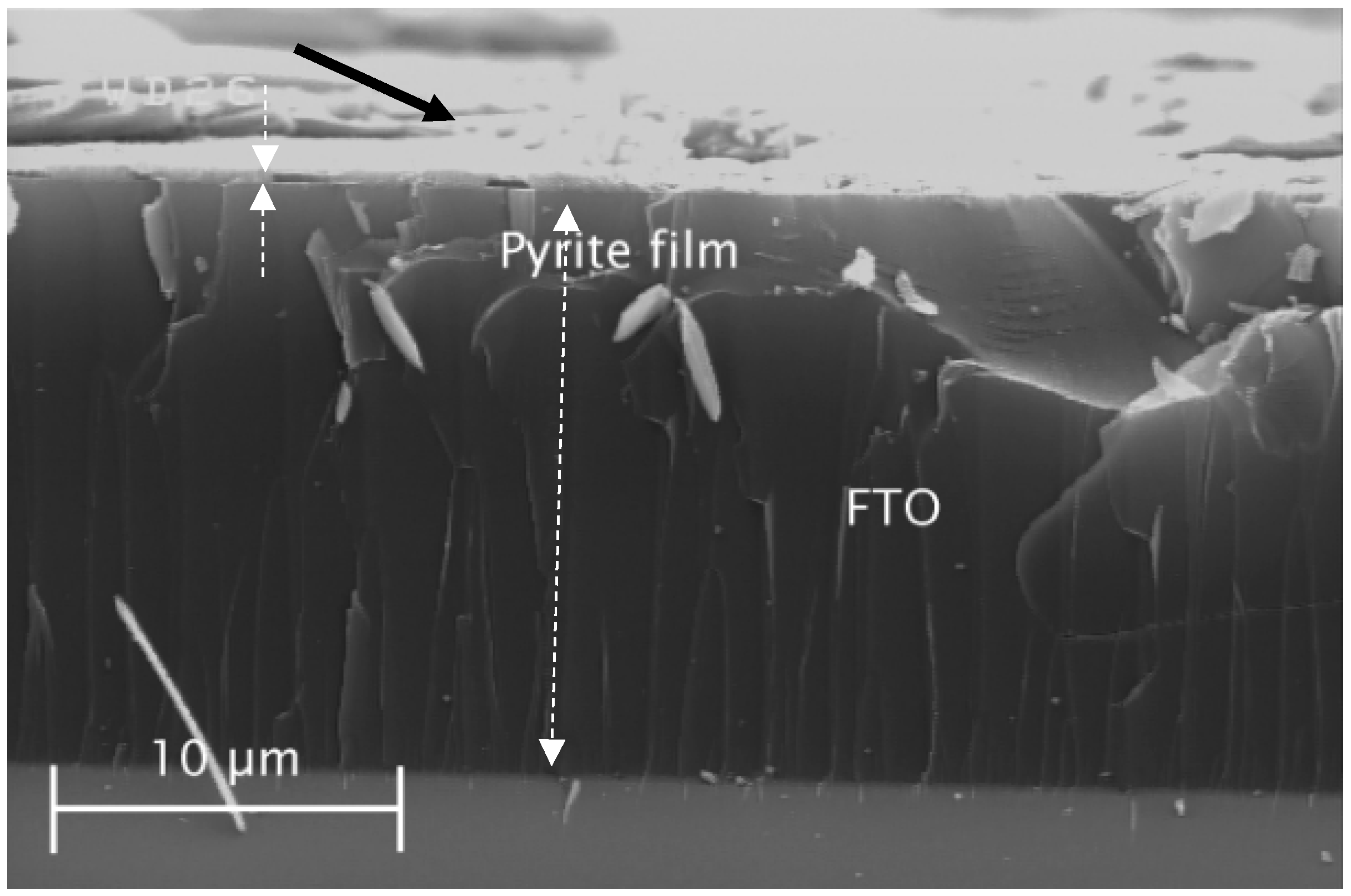
The color of all the powder and thin film samples turned black after sulfurization. The FESEM image of Sample G3 from the top view of the thin film sample showed the nano-rods, as depicted in
Figure 9. The diameter of the nano-rods was measured using an image software (ImageJ) and was
on average, which was two times larger than the thickness of akaganéite nano-rods. The thickness of this layer was between 400 and 700 nm according to its cross-section microscopic image shown in
Figure 10. Moreover, some impurities were deposited on the thin film which could be the sulfur condensed residuals, shown by a black arrow in
Figure 10. The XRD analysis of the powder sample (P3) showed an incomplete transformation of hematite to pyrite (FeS
2) after sulfurization (
Figure 11). The calculated crystallite size of pyrite crystals was
which was about 5 nm smaller than that of Sample P2 hematite crystallite size. Smaller pyrite crystals mean that not all of the hematite crystal was transformed to pyrite, and thus, the sulfurization time was insufficient. It has been reported that the main factor which affects the kinetics of the process is the diffusion rate of sulfur atoms into the hematite crystals and oxygen atoms out of it [
18].
Marcasite is an iron sulfide phase with an orthorhombic crystal structure. A Raman spectroscopy analysis is the only way to distinguish between marcasite and pyrite phases, and it was used in this report to characterize the thin film Sample G3, as shown in
Figure 12. It has been reported that the active Raman peaks of pyrite and marcasite are (353,387 cm
−1) and (324,387 cm
−1), respectively [
34]. Accordingly, the first peak of the sample could be assigned to marcasite, the second one to pyrite, and the third one to both of them which was overlapped. Therefore, the sample layer consisted of both pyrite and marcasite phases. Pyrite was the dominant phase due to the relative Raman peak intensities. The formation of the marcasite phase in this process could be justified by the uncontrollable partial pressure of gaseous pyrite in the silicon tube which could result in the stabilization of two marcasite and pyrite phases alongside.
A UV-Vis analysis was carried out for Sample G3 to investigate the optical properties. The high absorption obtained in the UV to the visible range of the light wavelength emphasizes that pyrite is a good choice for the absorption of sunlight (
Figure 13). In addition, no absorption peaks were observed in this range (313 to 1090 nm). In other words, the band gap of pyrite thin film is, at most, 1.127 eV.
The sulfurization process time varied and the Raman shifts of each sample were obtained (
Figure 14). The samples all show Raman active peaks of pyrite and marcasite but there are also some unrecognized peaks visible in the curves. To estimate the relative contents of pyrite and marcasite, the ratios of the first active Raman peaks of pyrite and marcasite for different samples were calculated and compared in the inset in
Figure 14. This ratio reveals that the sample with 1 h sulfurization time (F31) has the most pyrite to marcasite relative concentration.
A schematic representation of the cross-section of the final solar cell is shown in
Figure 15a. The structure consists of a thin film of pyrite which is sandwiched between an FTO-coated glass and a physical vapor-deposited aluminum layer. This is a Schottky-type solar cell in which a semiconductor (pyrite) is in contact with metal (aluminum). The aluminum and FTO layers also have the role of positive and negative electrodes, respectively.
The surface electrical resistance of pyrite,
, was measured as
, using a four-point probe ohmmeter. Furthermore, the calculated work function (
) of aluminum is
[
35] and the electron affinity (
) of pyrite is
[
36]. The estimated band diagram of the contact of pyrite and aluminum is drawn by considering the above parameters in
Figure 15b. The resulted band bending in the valence and conduction bands of pyrite in contact with the aluminum guide photoexcited electrons and holes toward the FTO and aluminum electrodes, respectively, before recombination occurs. This process completes the external circuit and produces electrical current. The maximum voltage that this cell can make is
, as shown in
Figure 15b.
The current-voltage behavior of each sample was measured in both dark and illuminated conditions. The resulting J-V curves are shown in
Figure 16. Samples F3.10 (
Figure 16a) and F36 (
Figure 16d) did not show any photovoltaic response, and in particular, no Schottky contacts were detected. The electrical shunts might be responsible for this, as the film formation process is not fully controlled, and thus, the pyrite thin film may not cover all the substrate. Notice that the pyrite thin film thickness is as low as 500 nm and it is not possible to be increased by this type of ACG process.
Furthermore, unknown Raman peaks, as can be observed in
Figure 14, can result from unknown chemical bonds that are formed during sulfurization. These conditions can cause new surface states or band defects which, in consequence, can lower the photoelectric response.
Samples F31 and F3.30 had photovoltaic responses according to
Figure 16b,c. The calculated energy conversion efficiencies (
) of Samples F31 and F3.30 were 0.0044 and 0.00025%, respectively, which were lower than the
values reported by Lin [
9] and Ennaoui [
18] and were consistent with those reported by Steinhagen [
26] and Bi [
25].
Nevertheless, the
value of the sample with 1 h sulfurization time (F31) is higher than those of the other samples. This can be related to the higher pyrite to marcasite ratio of this sample. It can be stated that the main reason for the low open-circuit voltage of these solar cells is the presence of marcasite impurity, as reported previously [
37]. Moreover, the formation of new surface states in pyrite can cause the recombination of excited electrons and holes before being collected in the external circuit [
2,
38].


 ,
, 


