

Eddy Current Testing of Artificial Defects in 316L Stainless Steel Samples Made by Additive Manufacturing Technology


Abstract
:1. Introduction
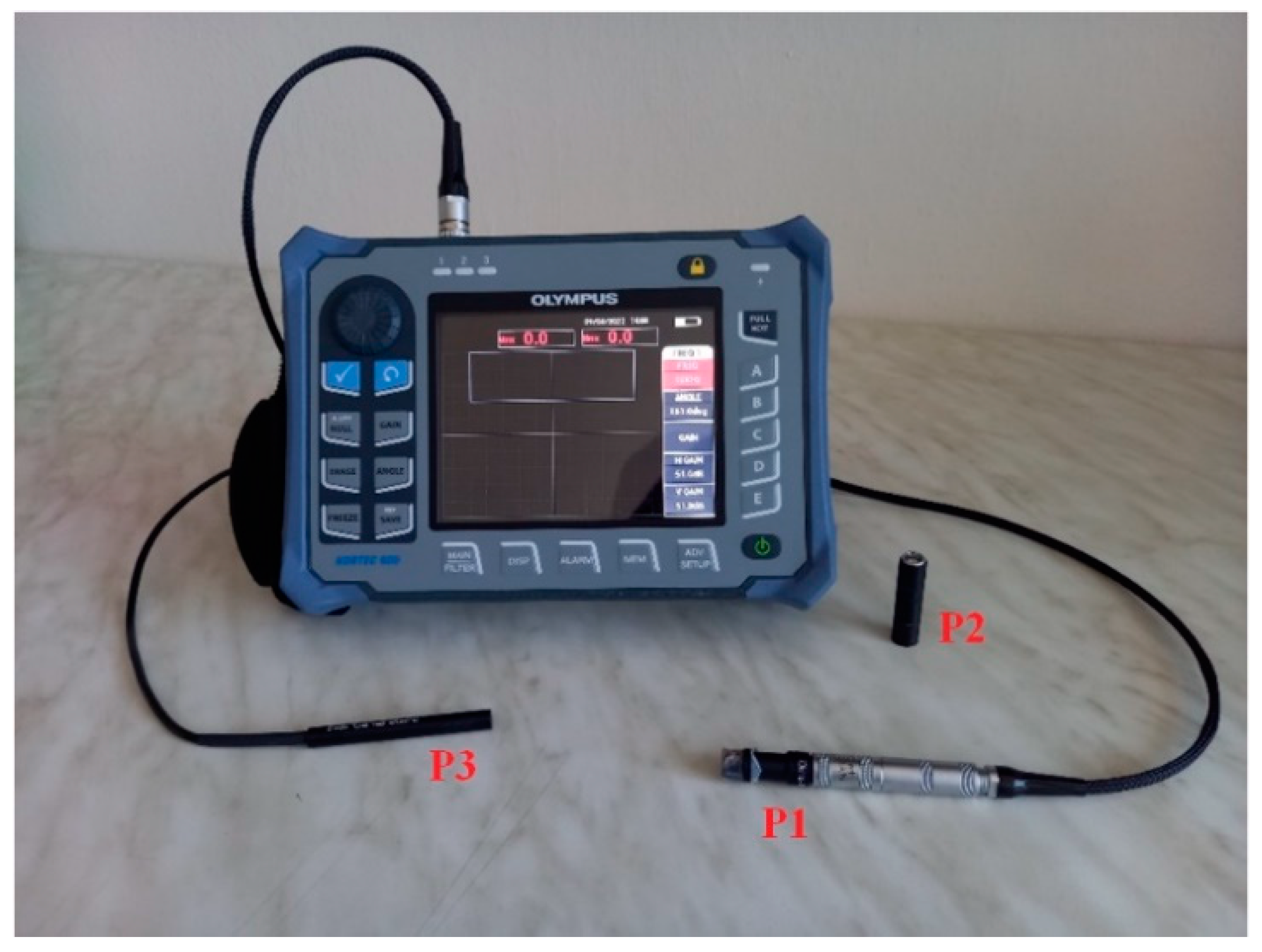
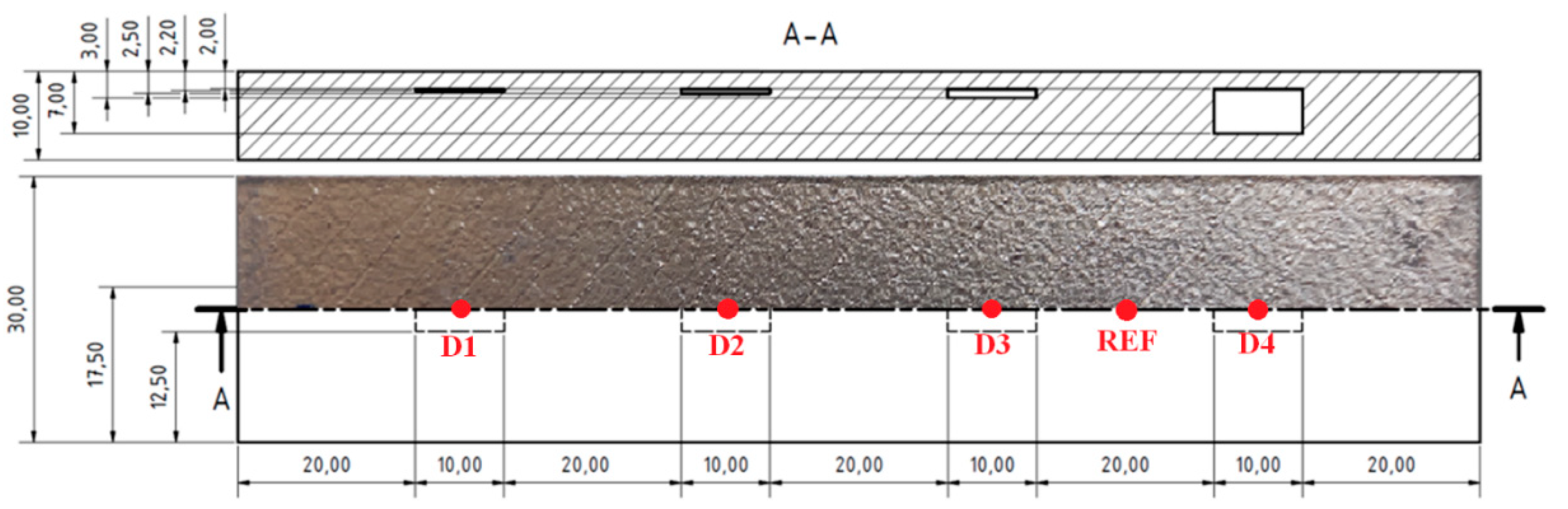
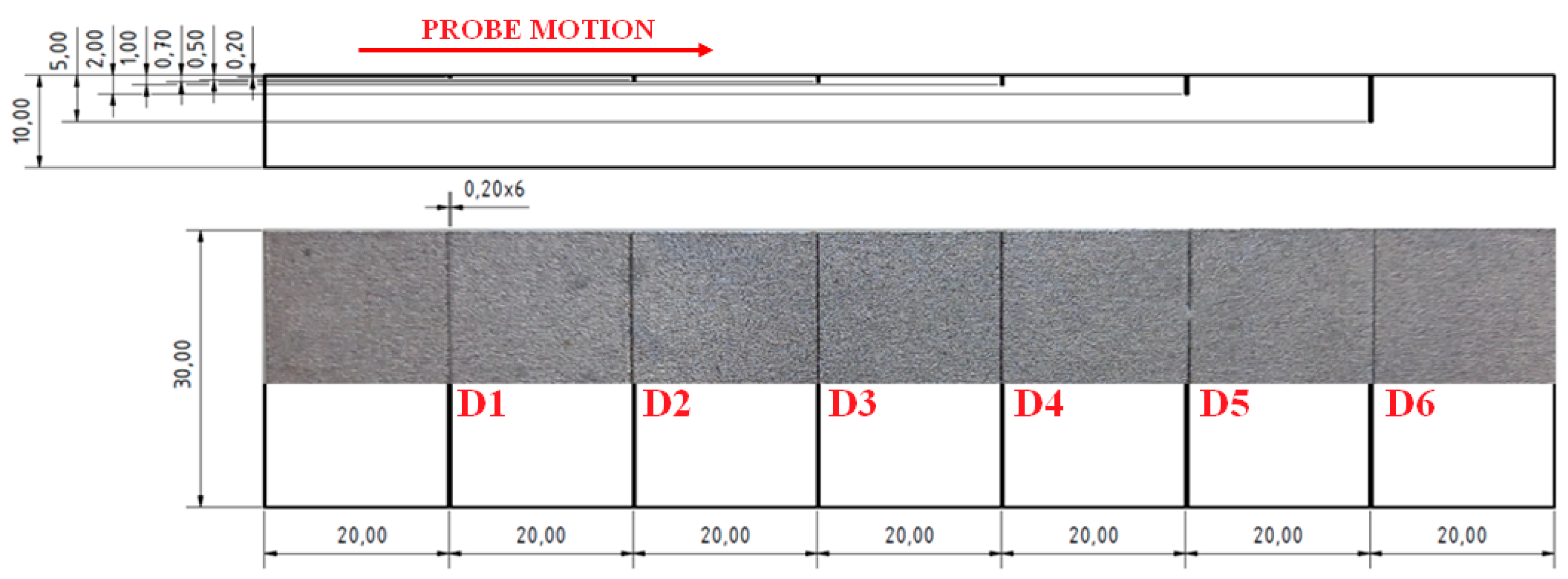
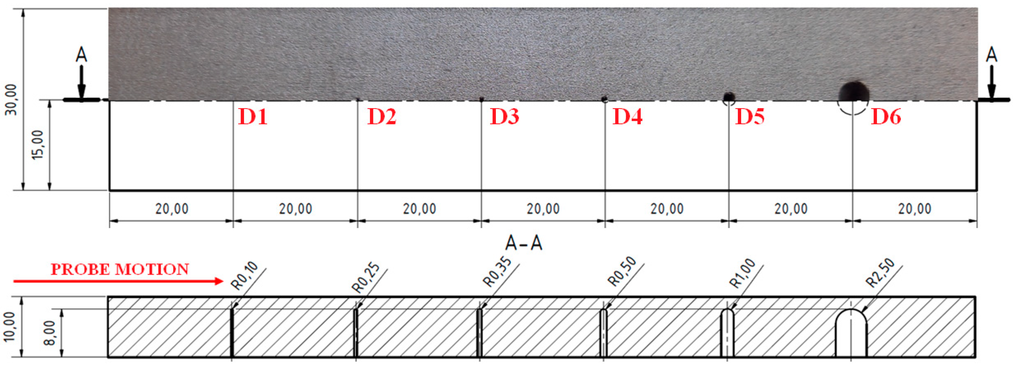
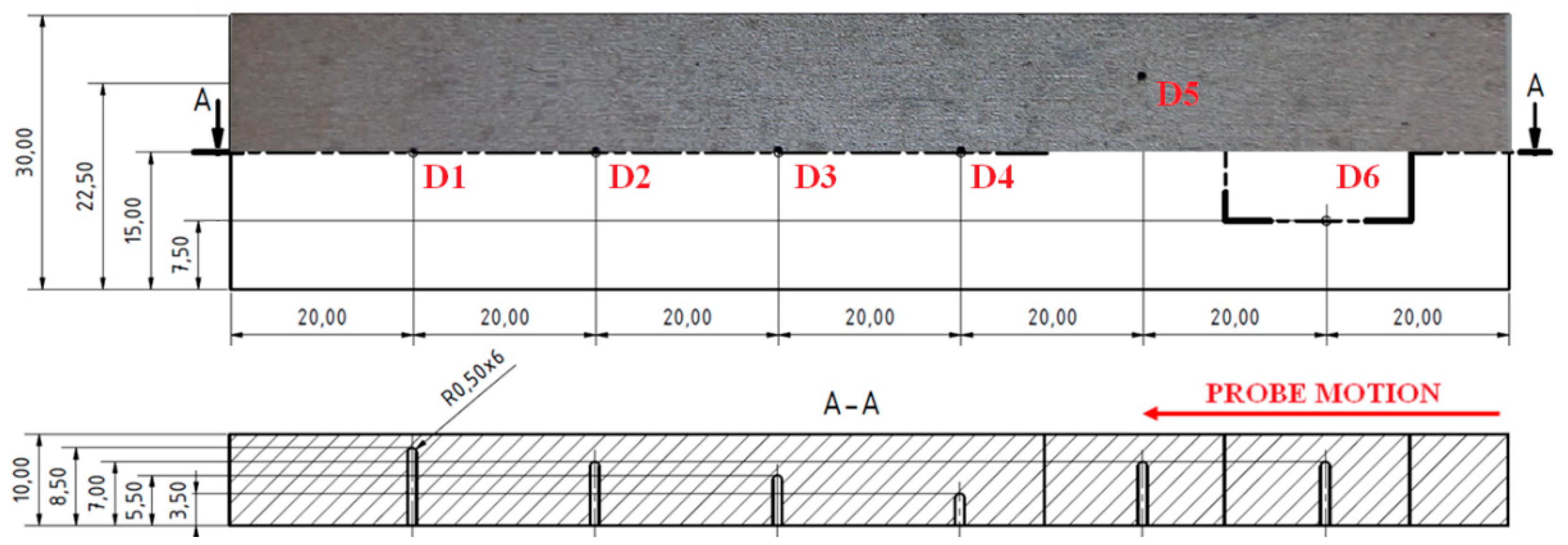
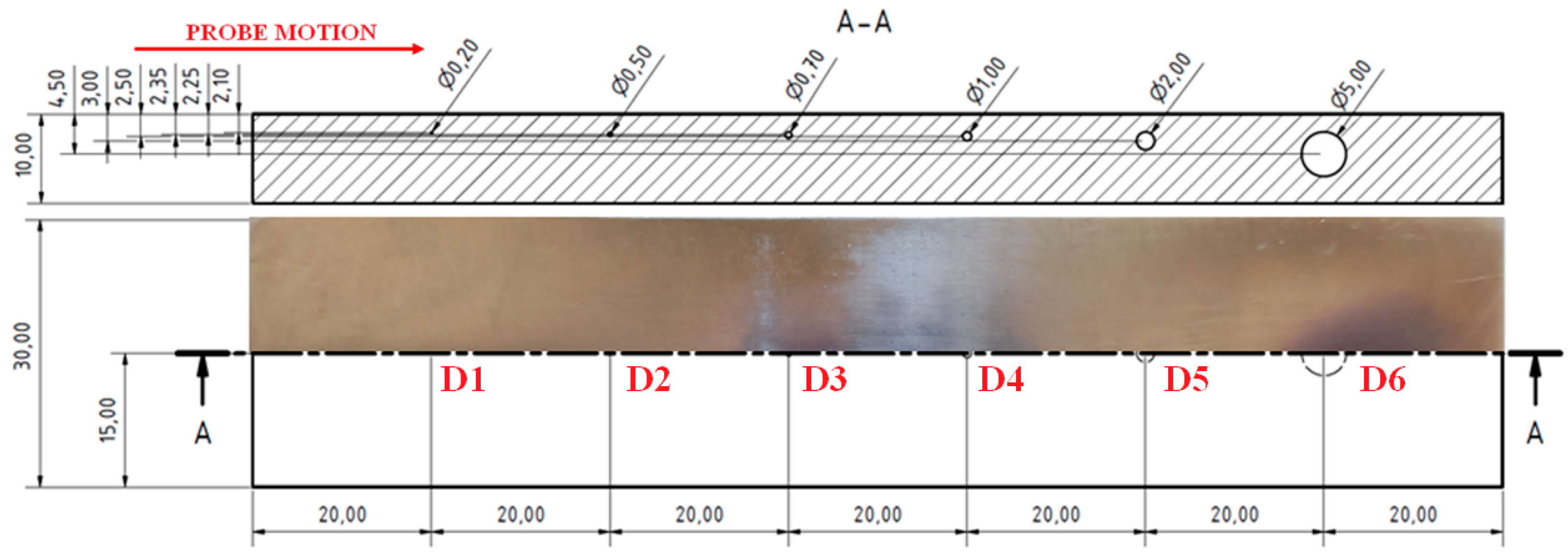
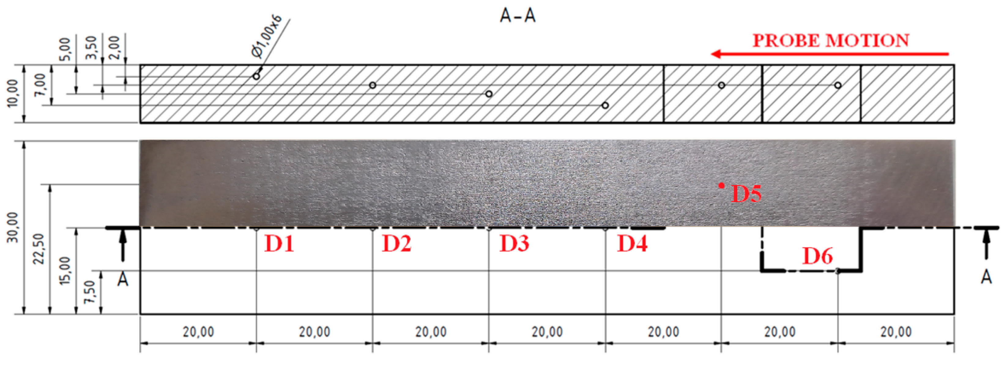
2. Materials and Methods
3. Results
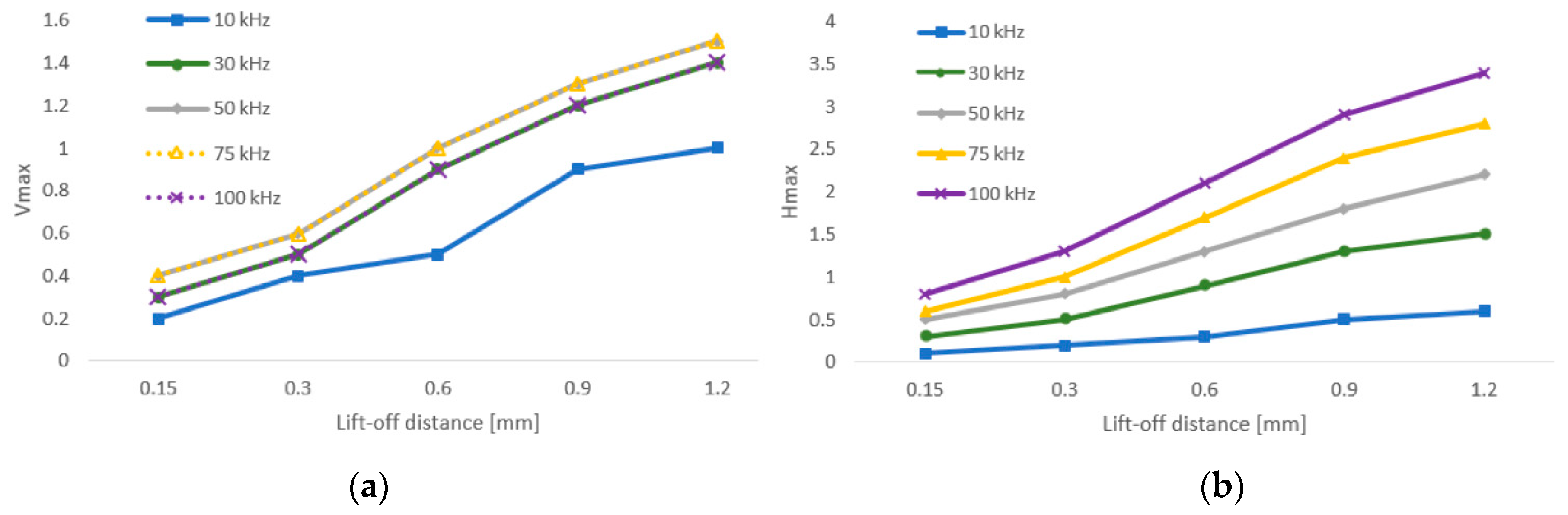
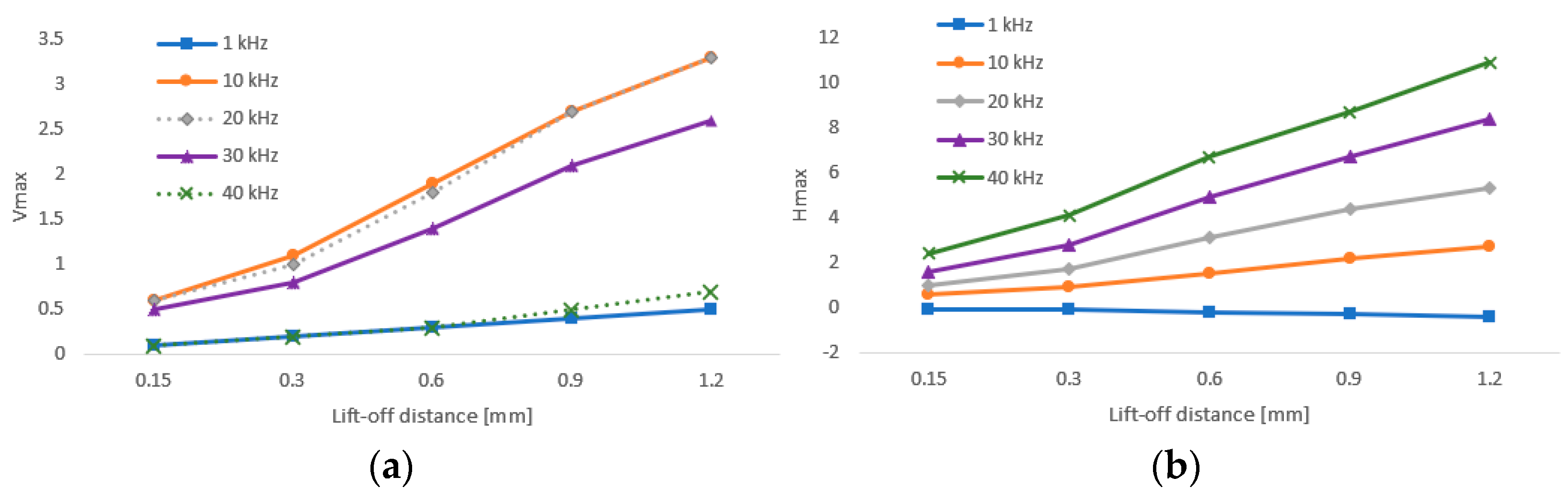
3.1. Lift-Off Effect Examination
3.2. Penetration Depth Calculation
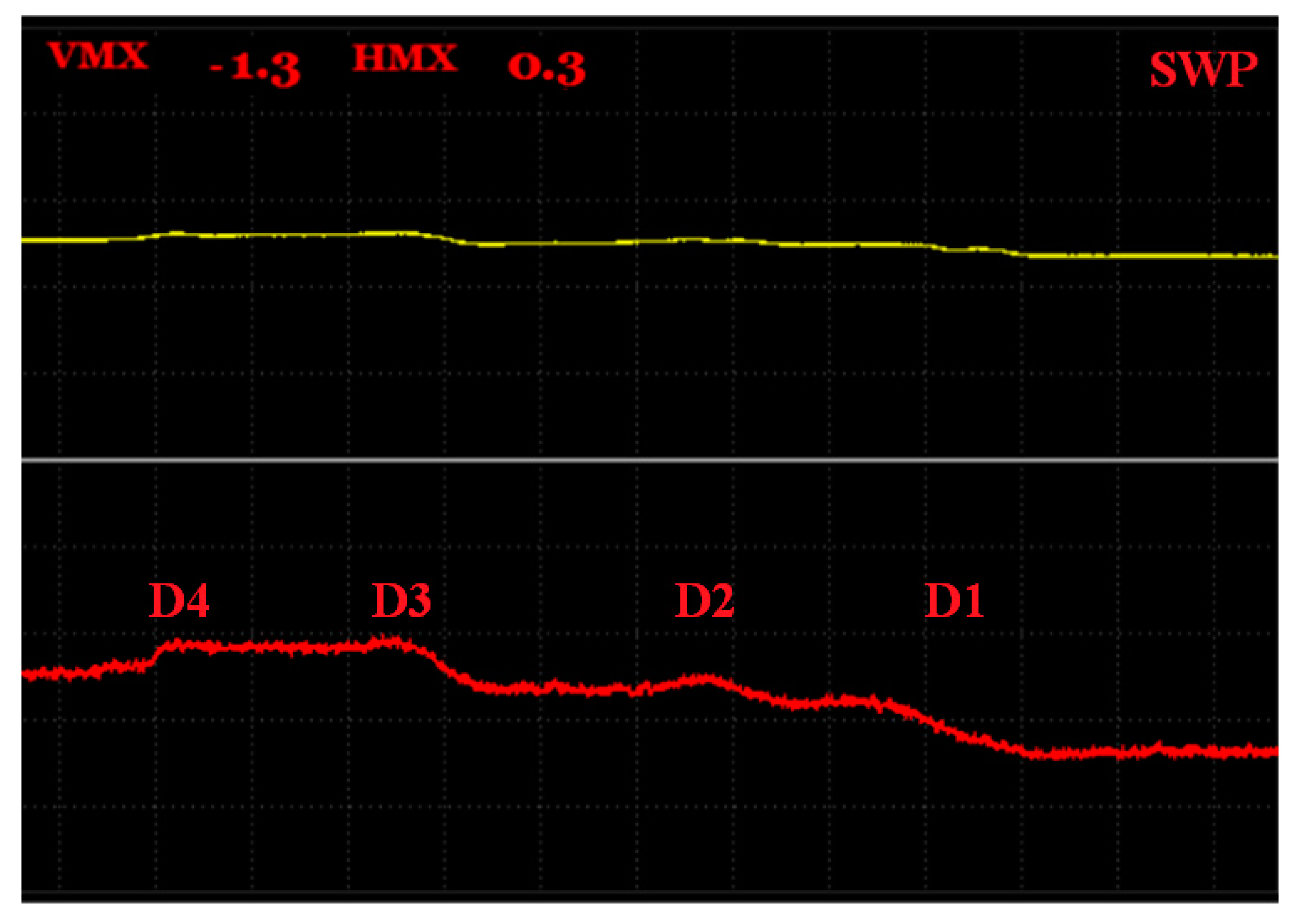
3.3. Artificial Defects Identification
3.3.1. S1 Sample
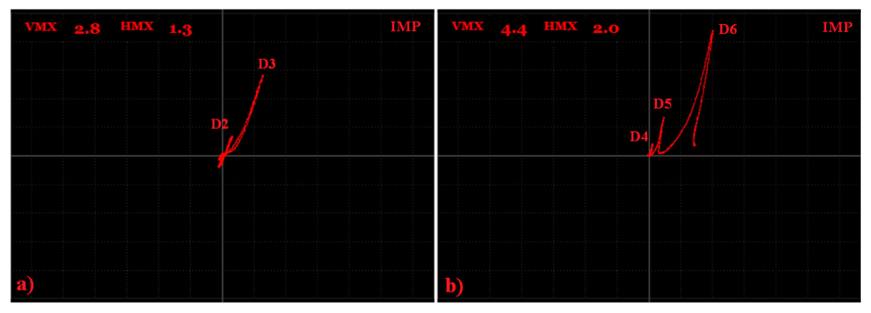
3.3.2. S2 Sample
3.3.3. S3 Sample
3.3.4. S4 Sample
3.3.5. S5 Sample
3.3.6. S6 Sample
4. Discussion
5. Conclusions
- Various reactance and resistance values, with various follow-up signal deviations according to the different shapes and sizes of the designed artificial defects in the article, prove that the eddy current non-destructive testing method has all the prerequisites for detecting defects in additively manufactured parts made of used material.
- For the experimental setup of the parameters of a measurement device, it is important to know if the evaluated defect reaches the surface of the material or if it is included in a subsurface layer. Same as in the case of the common eddy current testing of materials, a higher frequency and consequently a higher sensitivity can be set for the first mentioned, since the skin effect significantly affects the eddy current measurement.
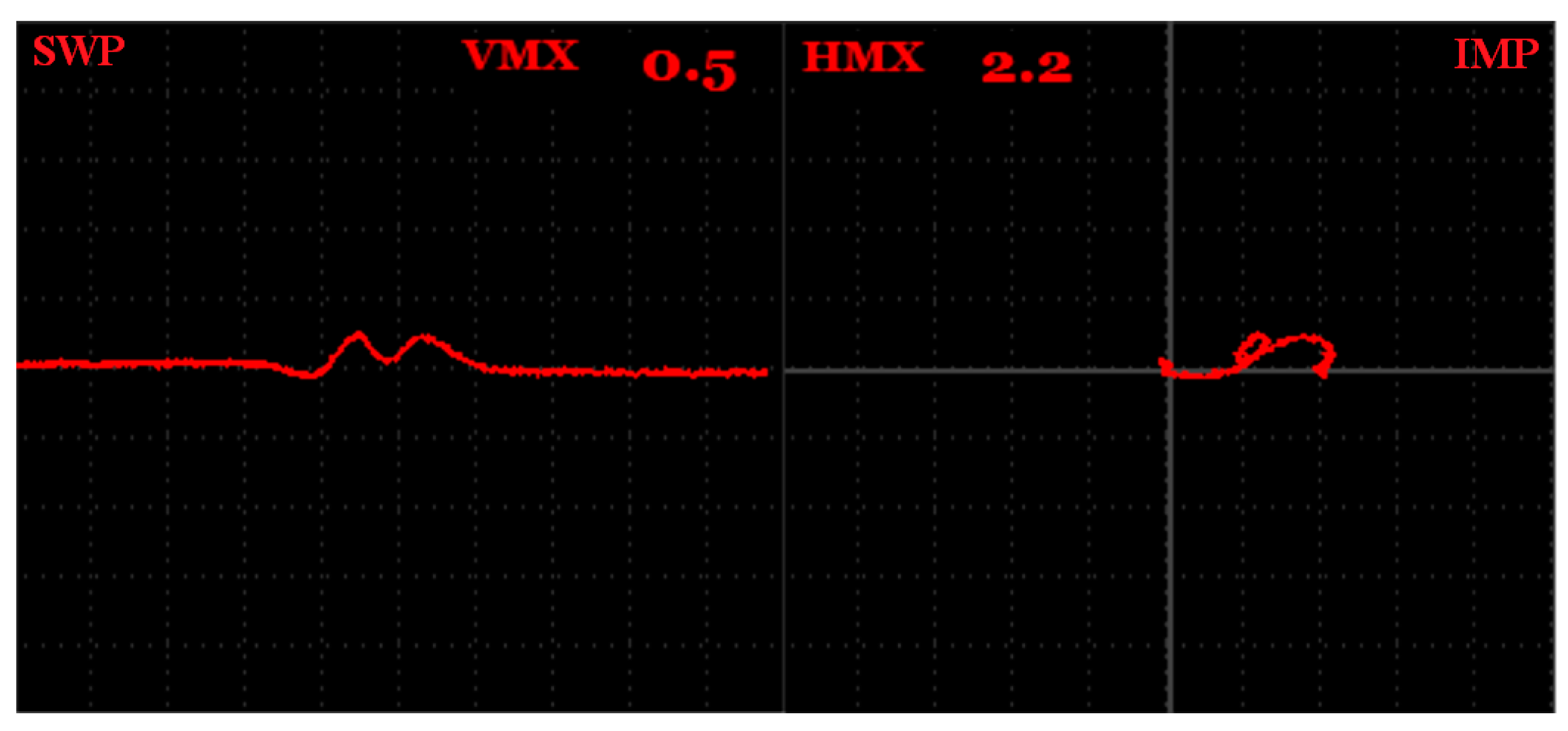
- Additionally, the selection of the available identification regimes (IMPEDANCE or SWEEP) is important, according to the defect kind. For the inner defects in the subsurface layer, the better choice is unequivocally the SWEEP mode because of the significantly higher noise and lift-off effect of the IMPEDANCE regime signal during the use of higher frequencies and GAIN values. On the other side, the IMPEDANCE mode is better for surface reaching defects because of its better depiction of the obtained data. For both regimes, it is positive to differ the setup according to the size of the defect, where a 1 mm diameter or depth (for the grooves) could be a boundary due to the high signal difference of the smaller and larger defects.
- As can be seen for samples S3 and S5, cavities with a 0.2 mm diameter were not printed, or were just partially printed. So, it is important to take the possibilities of printing technology into account. However, it can be stated that the smallest defect that can be detected has a 0.5 mm diameter and depth for the groove type. The highest reached depth of a place of defect can be 6.5 mm.
- Regarding the defect shape influence, for the groove type shape, a higher Vmax deviation and a stronger peak in the vertical direction was obtained, which applies to both regimes. In the case of the circular and spherical shapes, the Vmax and Hmax variations were not so different. For the SWP mode, double peaks were obtained and for the IMP mode, a wave-resembling curve was obtained. In both cases, the size of the peak depended on the size and depth of the defect.
- Another factor, which is a follow-up to a previous point, is the presence of powder in a cavity. If a defect is filled with powder, the signal is not influenced with such a magnitude as an empty one is. This is due to the smaller sensitivity of the eddy currents on a medium with some density compared to ones with empty space.
Author Contributions
Funding
Institutional Review Board Statement
Informed Consent Statement
Data Availability Statement
Acknowledgments
Conflicts of Interest
References
- Wong, K.V.; Hernandez, A. A review of additive manufacturing. Int. Sch. Res. Not. 2012, 2012, 208760. [Google Scholar] [CrossRef]
- Frazier, W.E. Metal additive manufacturing: A review. J. Mater. Eng. Perform. 2014, 23, 1917–1928. [Google Scholar] [CrossRef]
- Despa, V.; Gheorghe, I.G. Study of selective laser sintering: A qualitative and objective approach. Sci. Bull. Valahia Univ. Mater. Mech. 2011, 6, 150–155. [Google Scholar]
- Kellens, K.; Yasa, E.; Dewulf, W.; Duflou, J.R. Environmental assessment of selective laser melting and selective laser sintering. Methodology 2010, 4, 1–8. [Google Scholar]
- Röttger, A.; Boes, J.; Theisen, W.; Thiele, M.; Esen, C.; Edelmann, A.; Hellmann, R. Microstructure and mechanical properties of 316L austenitic stainless steel processed by different SLM devices. Int. J. Adv. Manuf. Technol. 2020, 108, 769–783. [Google Scholar] [CrossRef]
- Dong, Z.; Liu, Y.; Wen, W.; Ge, J.; Liang, J. Effect of hatch spacing on melt pool and as-built quality during selective laser melting of stainless steel: Modeling and experimental approaches. Materials 2018, 12, 50. [Google Scholar] [CrossRef] [PubMed]
- Marattukalam, J.J.; Karlsson, D.; Pacheco, V.; Beran, P.; Wiklund, U.; Jansson, U.; Hjörvarsson, B.; Sahlberg, M. The effect of laser scanning strategies on texture, mechanical properties, and site-specific grain orientation in selective laser melted 316L SS. Mater. Des. 2020, 193, 108852. [Google Scholar] [CrossRef]
- Chen, J.; Yang, Y.; Song, C.; Zhang, M.; Wu, S.; Wang, D. Interfacial microstructure and mechanical properties of 316L/CuSn10 multi-material bimetallic structure fabricated by selective laser melting. Mater. Sci. Eng. A 2019, 752, 75–85. [Google Scholar] [CrossRef]
- Kaynak, Y.; Kitay, O. The effect of post-processing operations on surface characteristics of 316L stainless steel produced by selective laser melting. Addit. Manuf. 2019, 26, 84–93. [Google Scholar] [CrossRef]
- Fu, J.; Li, H.; Song, X.; Fu, M. Multi-scale defects in powder-based additively manufactured metals and alloys. J. Mater. Sci. Technol. 2022, 122, 165–199. [Google Scholar] [CrossRef]
- Malekipour, E.; El-Mounayri, H. Common defects and contributing parameters in powder bed fusion AM process and their classification for online monitoring and control: A review. Int. J. Adv. Manuf. Technol. 2018, 95, 527–550. [Google Scholar] [CrossRef]
- Gu, D.; Shen, Y. Balling phenomena in direct laser sintering of stainless steel powder: Metallurgical mechanisms and control methods. Mater. Des. 2009, 30, 2903–2910. [Google Scholar] [CrossRef]
- Gong, H.; Rafi, K.; Gu, H.; Starr, T.; Stucker, B. Analysis of defect generation in Ti–6Al–4V parts made using powder bed fusion additive manufacturing processes. Addit. Manuf. 2014, 1, 87–98. [Google Scholar] [CrossRef]
- Hauser, C. Selective Laser Sintering of a Stainless Steel Powder. Ph.D. Thesis, University of Leeds, Leeds, UK, July 2003. [Google Scholar]
- Liu, Y.; Yang, Y.; Wang, D. A study on the residual stress during selective laser melting (SLM) of metallic powder. Int. J. Adv. Manuf. Technol. 2016, 87, 647–656. [Google Scholar] [CrossRef]
- Zhang, X.; Xiao, Z.; Yu, W.; Chua, C.K.; Zhu, L.; Wang, Z.; Xue, P.; Tan, S.; Wu, Y.; Zheng, H. Influence of erbium addition on the defects of selective laser-melted 7075 aluminium alloy. Virtual Phys. Prototyp. 2022, 17, 406–418. [Google Scholar] [CrossRef]
- Chen, H.; Gu, D.; Deng, L.; Lu, T.; Kühn, U.; Kosiba, K. Laser additive manufactured high-performance Fe-based composites with unique strengthening structure. J. Mater. Sci. Technol. 2021, 89, 242–252. [Google Scholar] [CrossRef]
- Romano, S.; Nezhadfar, P.; Shamsaei, N.; Seifi, M.; Beretta, S. High cycle fatigue behavior and life prediction for additively manufactured 17-4 PH stainless steel: Effect of sub-surface porosity and surface roughness. Theor. Appl. Fract. Mech. 2020, 106, 102477. [Google Scholar] [CrossRef]
- Li, S.; Wei, Q.; Shi, Y.; Zhu, Z.; Zhang, D. Microstructure characteristics of Inconel 625 superalloy manufactured by selective laser melting. J. Mater. Sci. Technol. 2015, 31, 946–952. [Google Scholar] [CrossRef]
- Fergani, O.; Berto, F.; Welo, T.; Liang, S.Y. Analytical modelling of residual stress in additive manufacturing. Fatigue Fract. Eng. Mater. Struct. 2017, 40, 971–978. [Google Scholar] [CrossRef]
- Slotwinski, J.A.; Garboczi, E.J.; Hebenstreit, K.M. Porosity measurements and analysis for metal additive manufacturing process control. J. Res. Natl. Inst. Stand. Technol. 2014, 119, 494–528. [Google Scholar] [CrossRef]
- Dai, T.; Jia, X.-J.; Zhang, J.; Wu, J.-F.; Sun, Y.-W.; Yuan, S.-X.; Ma, G.-B.; Xiong, X.-J.; Ding, H. Laser ultrasonic testing for near-surface defects inspection of 316L stainless steel fabricated by laser powder bed fusion. China Foundry 2021, 18, 360–368. [Google Scholar] [CrossRef]
- Zhan, Y.; Liu, C.; Zhang, J.J.; Mo, G.Z.; Liu, C.S. Measurement of residual stress in laser additive manufacturing TC4 titanium alloy with the laser ultrasonic technique. Mater. Sci. Eng. A 2019, 762, 138093. [Google Scholar] [CrossRef]
- Ito, K.; Kusano, M.; Demura, M.; Watanabe, M. Detection and location of microdefects during selective laser melting by wireless acoustic emission measurement. Addit. Manuf. 2021, 40, 101915. [Google Scholar] [CrossRef]
- Biddle, C.C. Theory of Eddy Currents for Nondestructive Testing. Retrosp. Theses Diss. 1976, 201, 1–84. [Google Scholar]
- He, Y.; Luo, F.; Pan, M.; Weng, F.; Hu, X.; Gao, J.; Liu, B. Pulsed eddy current technique for defect detection in aircraft riveted structures. NDT E Int. 2010, 43, 176–181. [Google Scholar] [CrossRef]
- Förster, F. Sensitive eddy-current testing of tubes for defects on the inner and outer surfaces. Non-Destr. Test. 1974, 7, 28–36. [Google Scholar] [CrossRef]
- Fukutomi, H.; Huang, H.; Takagi, T.; Tani, J. Identification of crack depths from eddy current testing signal. IEEE Trans. Magn. 1998, 34, 2893–2896. [Google Scholar] [CrossRef]
- Bowler, N.; Huang, Y. Electrical conductivity measurement of metal plates using broadband eddy-current and four-point methods. Meas. Sci. Technol. 2005, 16, 2193–2200. [Google Scholar] [CrossRef]
- Wang, Z.; Yu, Y. Thickness and conductivity measurement of multilayered electricity-conducting coating by pulsed eddy current technique: Experimental investigation. IEEE Trans. Instrum. Meas. 2018, 68, 3166–3172. [Google Scholar] [CrossRef]
- Abdou, A.; Bouchala, T.; Abdelhadi, B.; Guettafi, A.; Benoudjit, A. Nondestructive Eddy Current Measurement of Coating Thickness of Aeronautical Construction Materials. Instrum. Mes. Métrol. 2019, 18, 451–457. [Google Scholar] [CrossRef]
- Ricken, W.; Liu, J.; Becker, W.J. GMR and eddy current sensor in use of stress measurement. Sens. Actuators A Phys. 2001, 91, 42–45. [Google Scholar] [CrossRef]
- Botko, F.; Zajac, J.; Czan, A.; Radchenko, S.; Lehocka, D.; Duplak, J. Influence of residual stress induced in steel material on Eddy currents response parameters. In Proceedings of the International Scientific-Technical Conference MANUFACTURING, Poznan, Poland, 19–22 May 2019. [Google Scholar]
- García-Martín, J.; Gómez-Gil, J.; Vázquez-Sánchez, E. Non-destructive techniques based on eddy current testing. Sensors 2011, 11, 2525–2565. [Google Scholar] [CrossRef] [PubMed]
- Du, W.; Bai, Q.; Wang, Y.; Zhang, B. Eddy current detection of subsurface defects for additive/subtractive hybrid manufacturing. Int. J. Adv. Manuf. Technol. 2018, 95, 3185–3195. [Google Scholar] [CrossRef]
- Guo, S.; Ren, G.; Zhang, B. Subsurface Defect Evaluation of Selective-Laser-Melted Inconel 738LC Alloy Using Eddy Current Testing for Additive/Subtractive Hybrid Manufacturing. Chin. J. Mech. Eng. 2021, 34, 111. [Google Scholar] [CrossRef]
- Obaton, A.-F.; Lê, M.-Q.; Prezza, V.; Marlot, D.; Delvart, P.; Huskic, A.; Senck, S.; Mahé, E.; Cayron, C. Investigation of new volumetric non-destructive techniques to characterise additive manufacturing parts. Weld. World 2018, 62, 1049–1057. [Google Scholar] [CrossRef]
- Kobayashi, N.; Yamamoto, S.; Sugawara, A.; Nakane, M.; Tsuji, D.; Hino, T.; Terada, T.; Ochiai, M. Fundamental experiments of eddy current testing for additive manufacturing metallic material toward in-process inspection. AIP Conf. Proc. 2019, 2102, 070003. [Google Scholar]
- Özer, G.; Tarakçi, G.; Yilmaz, M.S.; Öter, Z.Ç.; Sürmen, Ö.; Akça, Y.; Coşkun, M.; Koç, E. Investigation of the effects of different heat treatment parameters on the corrosion and mechanical properties of the AlSi10Mg alloy produced with direct metal laser sintering. Mater. Corros. 2020, 71, 365–373. [Google Scholar] [CrossRef]
- Ehlers, H.; Pelkner, M.; Thewes, R. Heterodyne eddy current testing using magnetoresistive sensors for additive manufacturing purposes. IEEE Sens. J. 2020, 20, 5793–5800. [Google Scholar] [CrossRef]
- Duarte, V.R.; Rodrigues, T.A.; Machado, M.A.; Pragana, J.P.; Pombinha, P.; Coutinho, L.; Silva, C.M.; Miranda, R.M.; Goodwin, C.; Huber, D.E.; et al. Benchmarking of nondestructive testing for additive manufacturing. 3d Print. Addit. Manuf. 2021, 8, 263–270. [Google Scholar] [CrossRef]
- Stoll, P.; Gasparin, E.; Spierings, A.; Wegener, K. Embedding eddy current sensors into LPBF components for structural health monitoring. Prog. Addit. Manuf. 2021, 6, 445–453. [Google Scholar] [CrossRef]
- E Farag, H.; Toyserkani, E.; Khamesee, M.B. Non-Destructive Testing Using Eddy Current Sensors for Defect Detection in Additively Manufactured Titanium and Stainless-Steel Parts. Sensors 2022, 22, 5440. [Google Scholar] [CrossRef] [PubMed]
- D’Accardi, E.; Krankenhagen, R.; Ulbricht, A.; Pelkner, M.; Pohl, R.; Palumbo, D.; Galietti, U. Capability to detect and localize typical defects of laser powder bed fusion (L-PBF) process: An experimental investigation with different non-destructive techniques. Prog. Addit. Manuf. 2022, 1–18. [Google Scholar] [CrossRef]
- Center of 3D Printing Protolab. Available online: https://protolab.cz (accessed on 3 August 2022).
- Data Sheet: SS 316L-0407 Powder for Additive Manufacturing. Available online: https://www.renishaw.com/resourcecentre/en/details/data-sheet-ss-316l-0407-powder-for-additive-manufacturing--90802 (accessed on 3 August 2022).
- NORTEC 600 Eddy Current Flaw Detector User’s Manual. Available online: https://manualzz.com/doc/59581713/olympus-nortec-600-user-manual (accessed on 3 August 2022).
- AISI Type 316L Stainless Steel. Available online: https://www.matweb.com/search/DataSheet.aspx?MatGUID=a2d0107bf958442e9f8db6dc9933fe31 (accessed on 3 August 2022).
- 304 Stainless Steel. Available online: https://www.matweb.com/search/DataSheet.aspx?MatGUID=abc4415b0f8b490387e3c922237098da (accessed on 3 August 2022).
- Aluminum 7075-T6. Available online: https://www.matweb.com/search/DataSheet.aspx?MatGUID=4f19a42be94546b686bbf43f79c51b7d (accessed on 3 August 2022).


| Element | Fe | Cr | Ni | Mo | Mn | Si | N | O | P | C | S |
|---|---|---|---|---|---|---|---|---|---|---|---|
| Mass (%) | Balance | 16–18 | 10–14 | 2–3 | ≤2 | ≤1 | ≤0.1 | ≤0.1 | ≤0.045 | ≤0.03 | ≤0.03 |
| Frequency f [Hz] | Standard Penetration Depth δ [mm] | |
|---|---|---|
| AISI 316L | SS 316L | |
| 500 | 19.36 | 16.03 |
| 1000 | 13.69 | 11.33 |
| 2000 | 9.68 | 8.01 |
| 3000 | 7.9 | 6.54 |
| 4000 | 6.84 | 5.67 |
| 5000 | 6.12 | 5.07 |
| 6000 | 5.59 | 4.63 |
| 7000 | 5.17 | 4.28 |
| 8000 | 4.84 | 4.01 |
| 9000 | 4.56 | 3.78 |
| 10,000 | 4.33 | 3.58 |
| 20,000 | 3.06 | 2.53 |
| 30,000 | 2.5 | 2.07 |
| 40,000 | 2.16 | 1.79 |
| 50,000 | 1.94 | 1.6 |
| 60,000 | 1.77 | 1.46 |
| 70,000 | 1.64 | 1.35 |
| 80,000 | 1.53 | 1.27 |
| 90,000 | 1.44 | 1.19 |
| 100,000 | 1.37 | 1.13 |
| Sample | Defects | f [Hz] | Hgain [dB] | Vgain [dB] | Angle [°] | Depth [mm] | DSP MODE |
|---|---|---|---|---|---|---|---|
| S1 | D1, D2, D3, D4 | 30,000 | 42.4 | 64 | 225 | 2.07 | IMP |
| S2 | D2, D3 | 90,000 | 64.5 | 63.5 | 134 | 1.19 | IMP |
| D4, D5, D6 | 5000 | 71 | 71 | 161 | 5.07 | IMP | |
| S3 | D2, D3 | 15,000 | 65 | 74 | 145 | 2.93 | SWP |
| D4, D5, D6 | 10,000 | 65 | 74 | 135; 85(D4) | 3.58 | SWP | |
| S3 (reversed) | D5, D6 | 10,000 | 63 | 58.5 | 180 | 3.58 | IMP |
| S4 | D1, D2, D3, D4 | 15,000 | 65 | 76 | 115 | 2.93 | SWP |
| S5 | D2, D3, D4 | 50,000 | 66 | 77 | 40 | 1.6 | SWP |
| D5, D6 | 15,000 | 65 | 75 | 90 | 2.93 | SWP | |
| S6 | D1, D2, D3, D4 | 25,000 | 66 | 77 | 105 | 2.27 | SWP |
| Sample | Vmax | Hmax | ||||||||||
|---|---|---|---|---|---|---|---|---|---|---|---|---|
| D1 | D2 | D3 | D4 | D5 | D6 | D1 | D2 | D3 | D4 | D5 | D6 | |
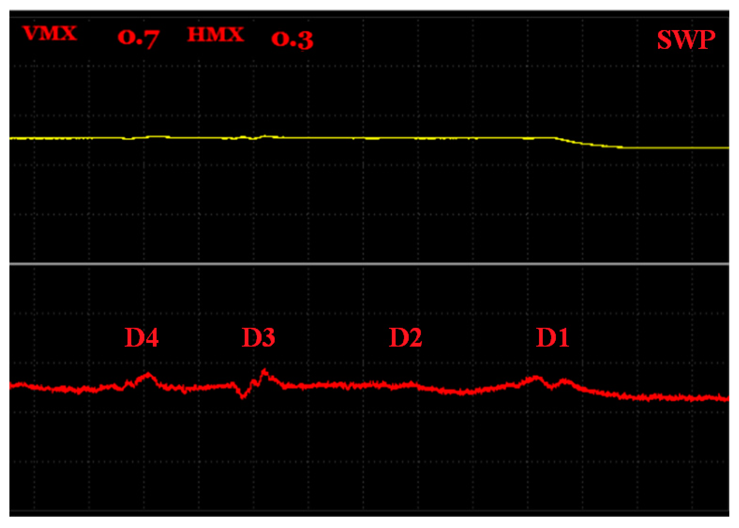
| S1 | −0.1 | −0.6 | −1.5 | −3.0 | - | - | 0 | 0 | 0 | 0 | - | - |
| S2 | - | 0.8 | 2.8 | 0.4 | 1.3 | 4.4 | - | 0.4 | 1.3 | 0.1 | 0.4 | 2.0 |
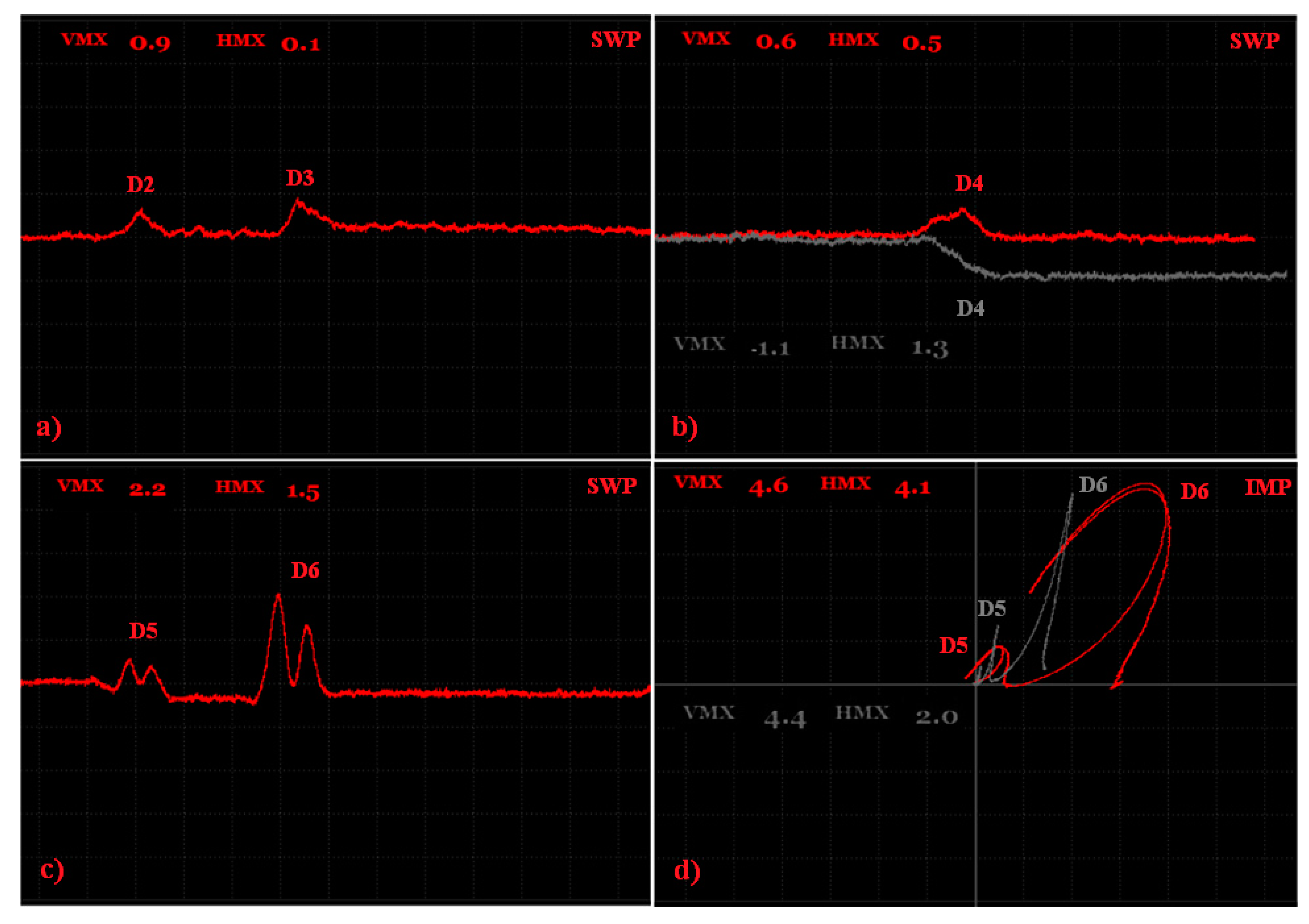
| S3 | - | 0.8 | 0.9 | −1.1/0.6 | 0.7 | 2.2 | - | 0.1 | 0.1 | 0.3/0.5 | 0.3 | 1.5 |
| S4 | 0.7 | −0.4 | 0.6 | 0.4 | - | - | 0.3 | 0.1 | −0.1 | −0.1 | - | - |
| S5 | - | 0.3 | 0.4 | 0.6 | −0.7 | 2.9 | - | −0.4 | −0.9 | 0.6 | 0.5 | 1.3 |
| S6 | −1.3 | −0.7 | −1.1 | 0.9 | - | - | 0.3 | 0.1 | 0.2 | −0.2 | - | - |
Publisher’s Note: MDPI stays neutral with regard to jurisdictional claims in published maps and institutional affiliations. |
© 2022 by the authors. Licensee MDPI, Basel, Switzerland. This article is an open access article distributed under the terms and conditions of the Creative Commons Attribution (CC BY) license (https://creativecommons.org/licenses/by/4.0/).
Share and Cite
Geľatko, M.; Hatala, M.; Botko, F.; Vandžura, R.; Hajnyš, J. Eddy Current Testing of Artificial Defects in 316L Stainless Steel Samples Made by Additive Manufacturing Technology. Materials 2022, 15, 6783. https://doi.org/10.3390/ma15196783
Geľatko M, Hatala M, Botko F, Vandžura R, Hajnyš J. Eddy Current Testing of Artificial Defects in 316L Stainless Steel Samples Made by Additive Manufacturing Technology. Materials. 2022; 15(19):6783. https://doi.org/10.3390/ma15196783
Chicago/Turabian StyleGeľatko, Matúš, Michal Hatala, František Botko, Radoslav Vandžura, and Jiří Hajnyš. 2022. "Eddy Current Testing of Artificial Defects in 316L Stainless Steel Samples Made by Additive Manufacturing Technology" Materials 15, no. 19: 6783. https://doi.org/10.3390/ma15196783
APA StyleGeľatko, M., Hatala, M., Botko, F., Vandžura, R., & Hajnyš, J. (2022). Eddy Current Testing of Artificial Defects in 316L Stainless Steel Samples Made by Additive Manufacturing Technology. Materials, 15(19), 6783. https://doi.org/10.3390/ma15196783