
Piezoelectric Response and Substrate Effect of ZnO Nanowires for Mechanical Energy Harvesting in Internet-of-Things Applications

 , , , , ,
  and
and
Abstract
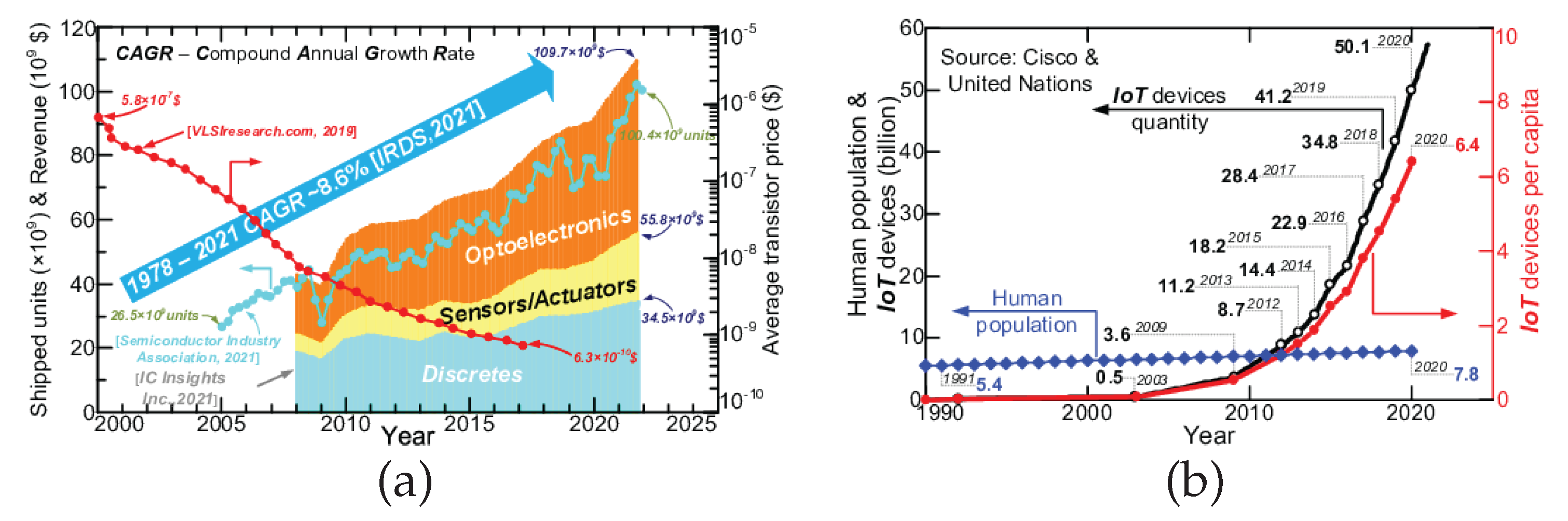
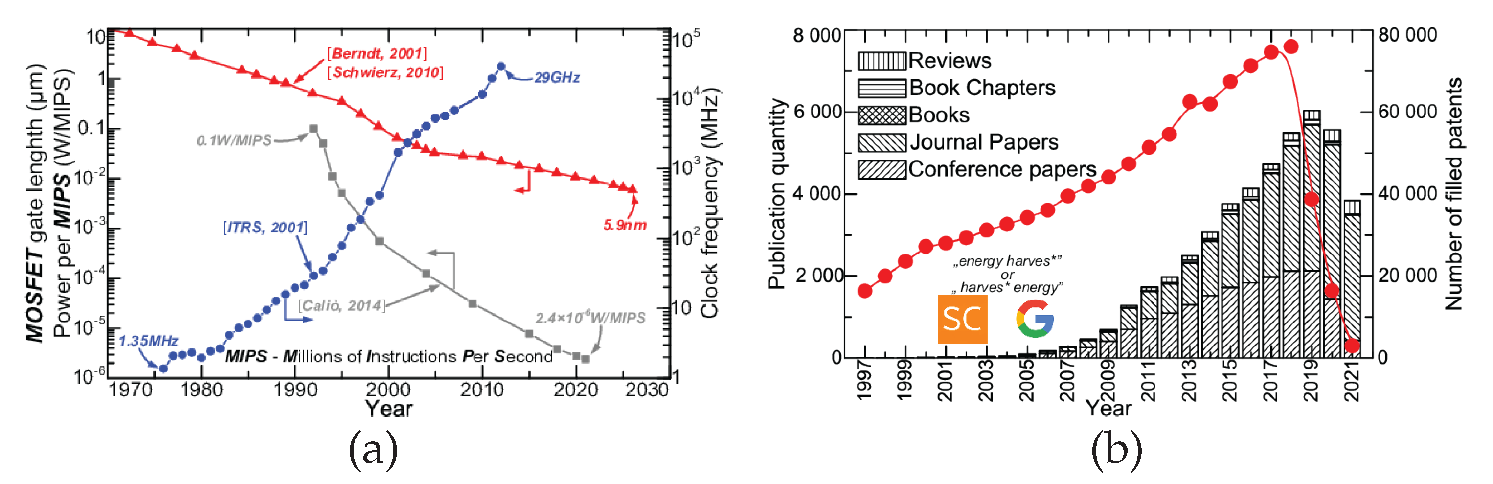
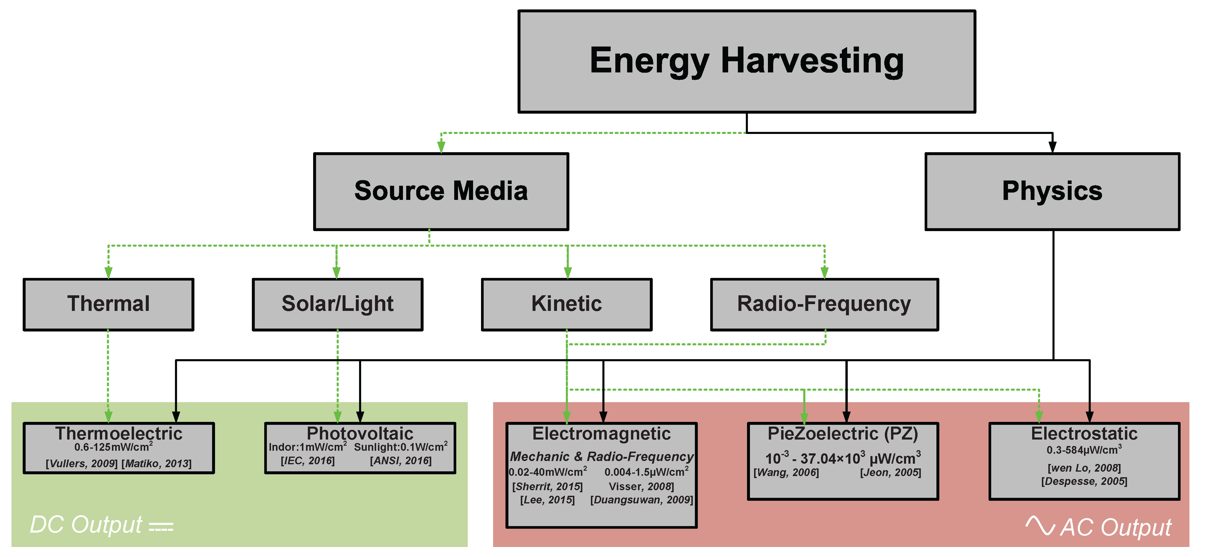
1. Introduction

| f | Excitation | Mass | Volume | P | Power Density | Material | Reference |
|---|---|---|---|---|---|---|---|
| (Hz) | (m/) | (g) | (cm) | (W) | (W/cm) | ||
| 0.5 | N/A | 1.2 | 0.101 | 0.25 | 2.47 | PZT-5H | [52] |
| 1.1 | N/A | N/A | 25 | 8400 | 336 | PZT | [44] |
| 100 | 72.7 | 0.96 | 0.20 | 35.5 | 16.3 | PZT | [48] |
| 120 | 2.5 | 9.2 | 1 | 375 | 375 | PZT | [46] |
| 120 | 0.98 | N/A | N/A | 500 | N/A | PMNZT | [67] |
| 13.9 | 106 | N/A | 27·10 | 1 | 37.04·10 | PZT | [49] |
| 1500 | 3.92 | 9·10 | 0.005 | 0.03 | 60 | AlN | [68] |
| N/A | N/A | N/A | 8.19·10 | 9.24·10 | 11.28 | AlN | [65] |
| 230 | 9.8 | N/A | N/A | 0.27 | N/A | PZT | [55] |
| 40 | 2.5 | 52.2 | 4.8 | 1700 | 700 | PZT | [50] |
| 462.5 | 19.6 | N/A | N/A | 2.15 | N/A | PZT | [56] |
| 50 | N/A | N/A | 9 | 180 | 20 | PZT | [51] |
| 56 | N/A | 228 | 113 | 1·10 | 2650 | P1-89 PZT | [54] |
| 608 | 9.8 | 0.0016 | 0.0006 | 2.16 | 3600 | PZT | [53] |
| 67 | 4 | 2.8 | 0.987 | 240 | 243.1 | PZT | [57] |
| 7000 | N/A | N/A | N/A | 1600 | N/A | PZT-PIC255 | [47] |
| 80 | 2.3 | 0.8 | 0.128 | 2.1 | 16.4 | PZT | [45] |
| 1 | N/A | N/A | 0.04 | 5.6 | 140 | PZT/PVDF | [58] |
| 3 | N/A | N/A | N/A | 1.296·10 | 2.47 | PVDF micro wall | [64] |
| N/A | N/A | N/A | 0.045 | 1.03 | 22.8 | ZnO NWs | [63] |
| N/A | N/A | N/A | 0.13·10 | 0.1·10 | 1.28 | ZnO NWs on paper | [61] |
| N/A | N/A | N/A | N/A | N/A | 1·10 | ZnO NWs | [59] |
| N/A | N/A | N/A | N/A | N/A | 10 | ZnO NWs | [60] |
| 3 | N/A | N/A | N/A | N/A | 144 | ZnO NWs | [62] |
| 1.63 | N/A | N/A | 4.51·10 | 1.38·10 | 3.1 | ZnO NWs on steel | (this work) |
2. Materials and Methods
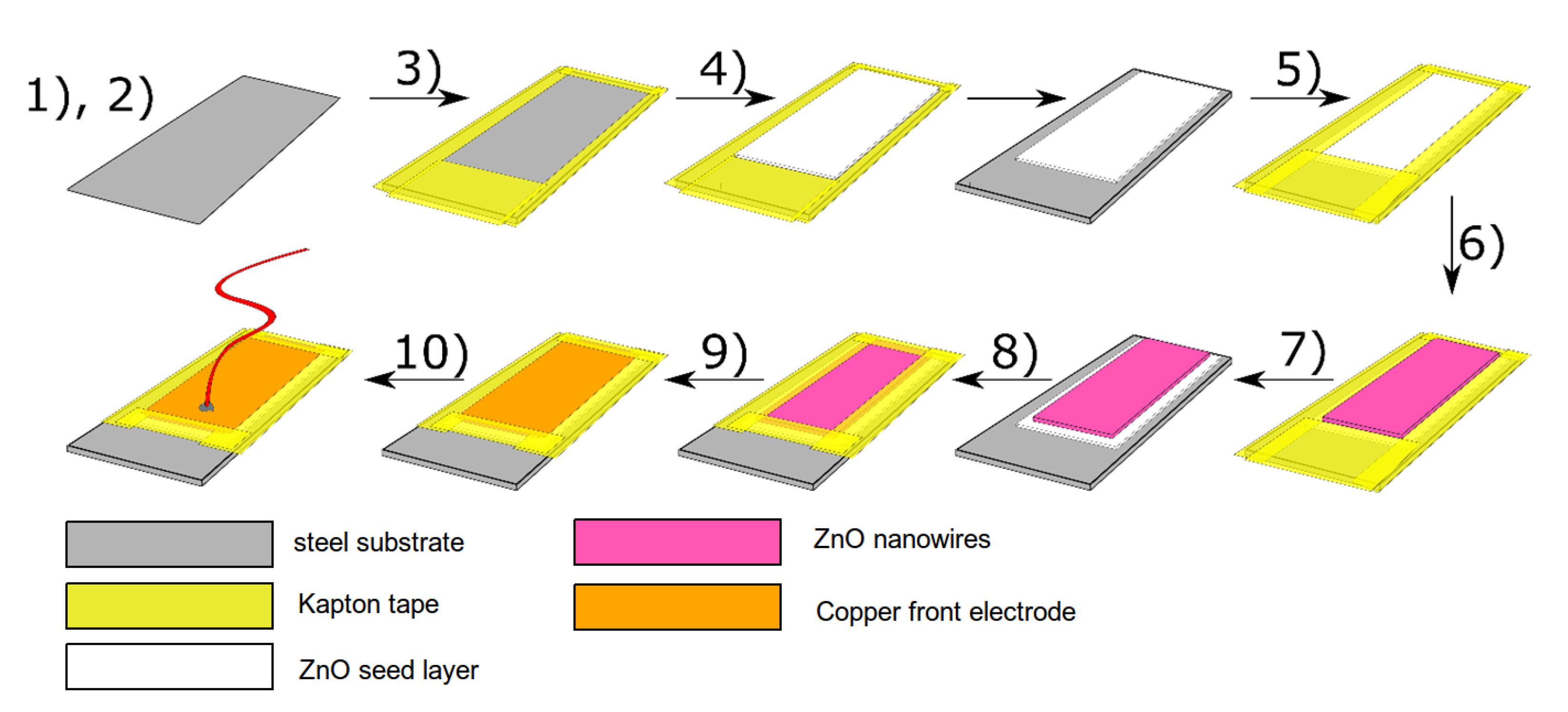
2.1. Sample Fabrication
2.1.1. Substrate
2.1.2. Synthesis
2.2. Characterization
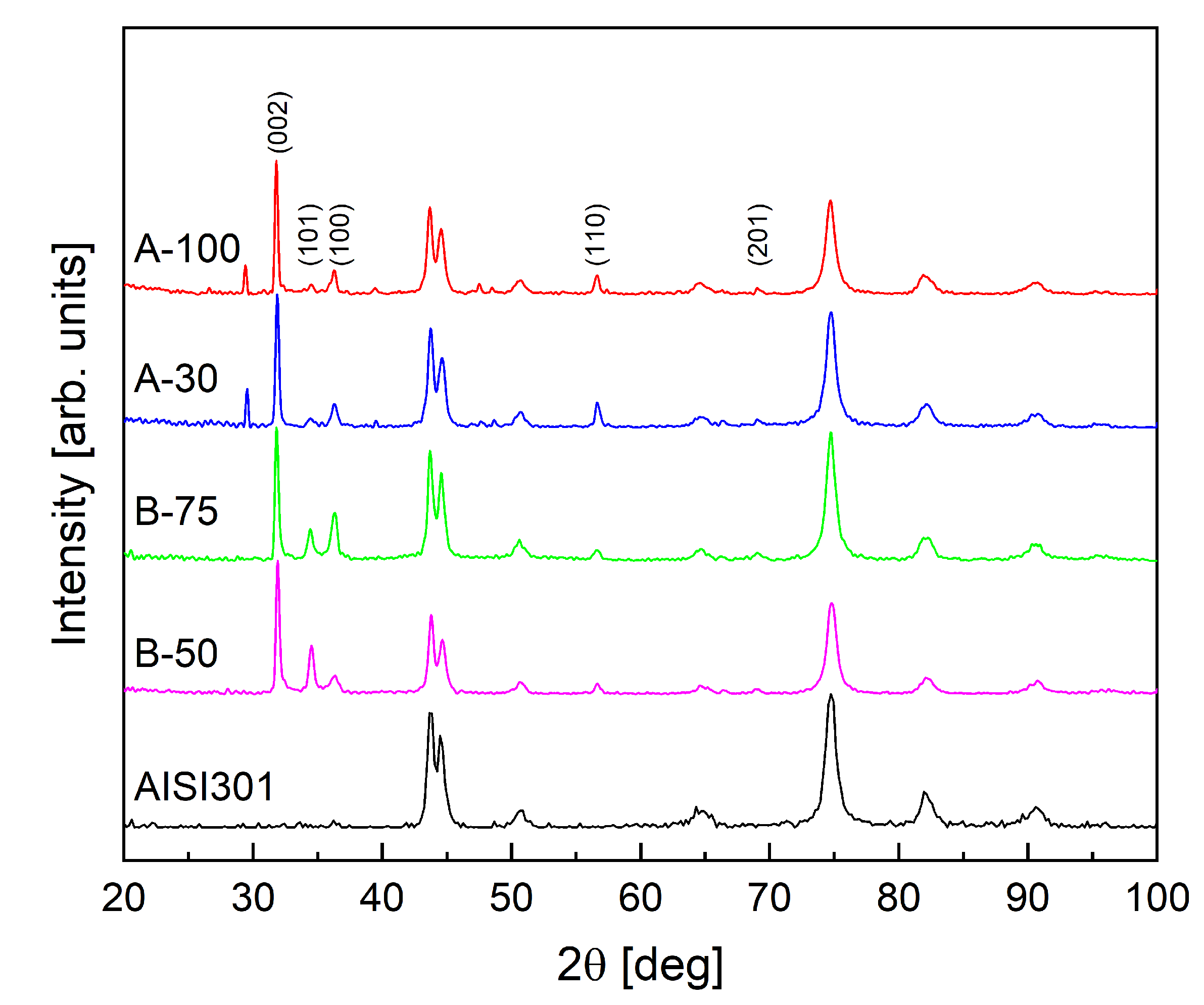
2.2.1. X-ray Diffraction
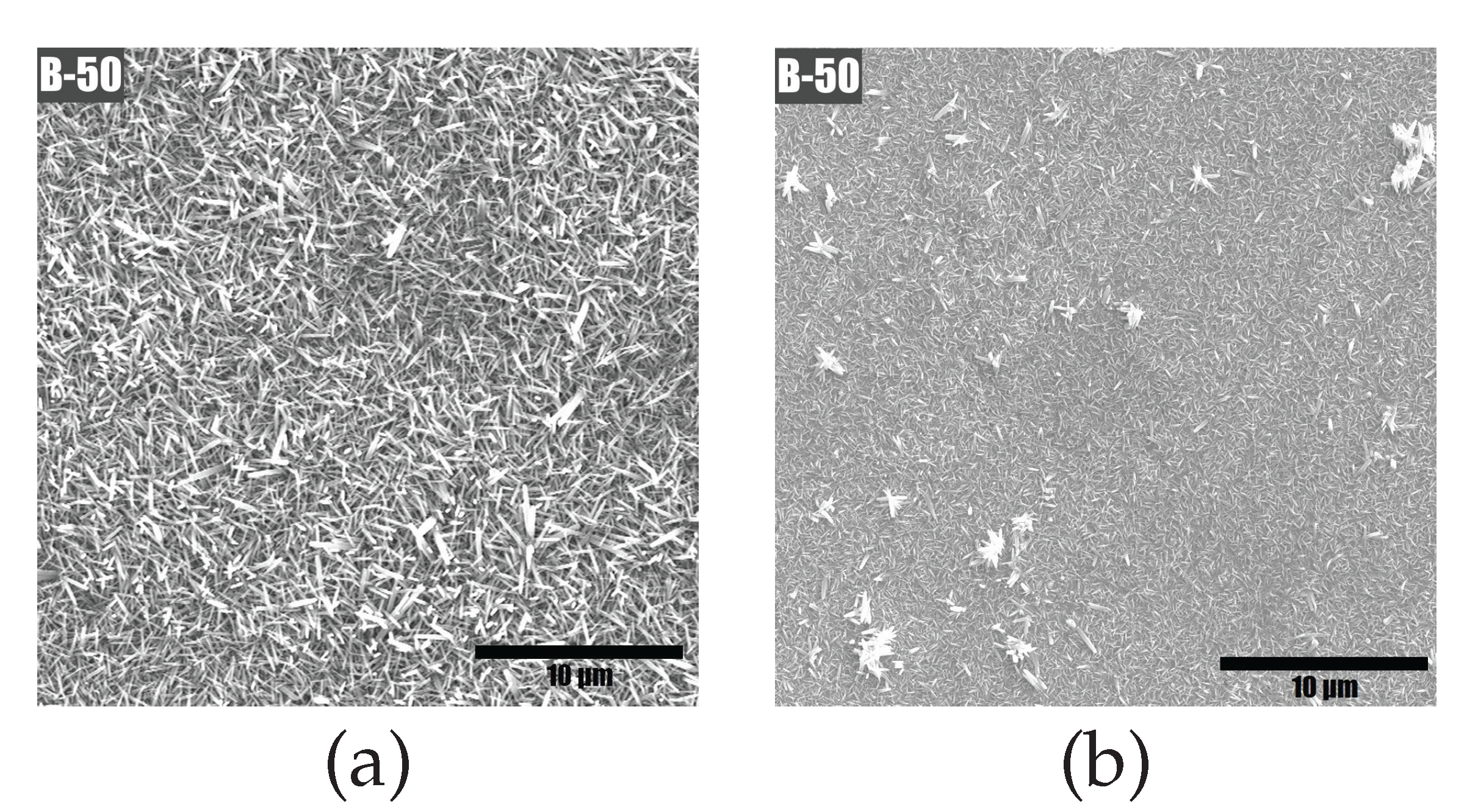
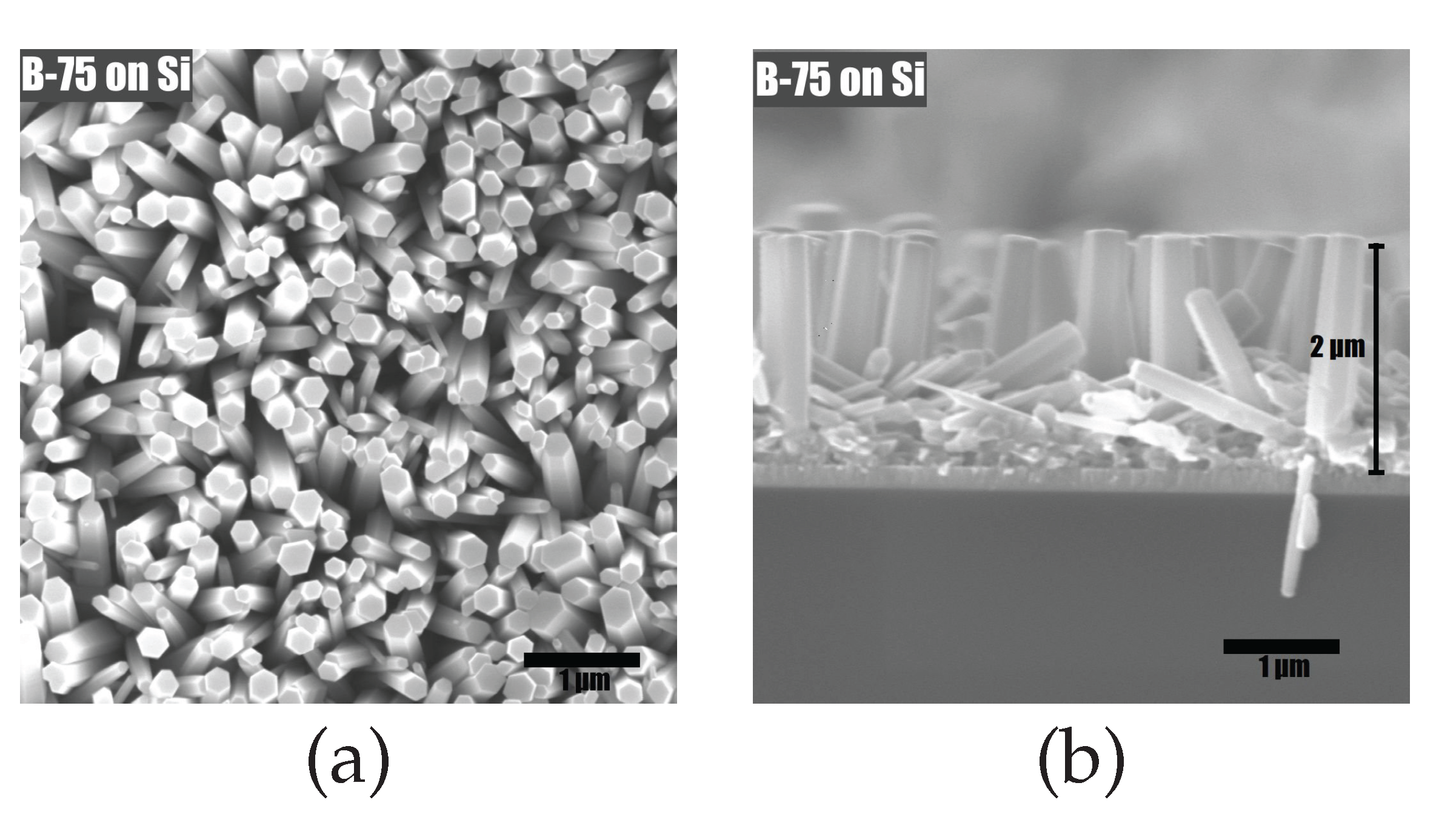
2.2.2. SEM
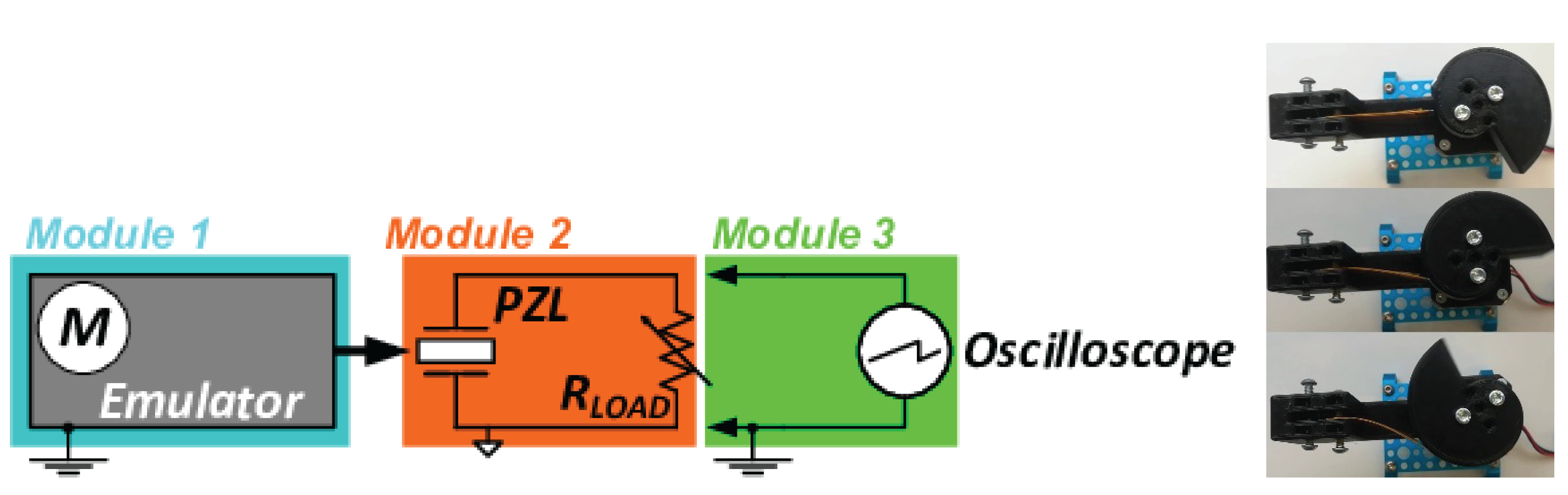
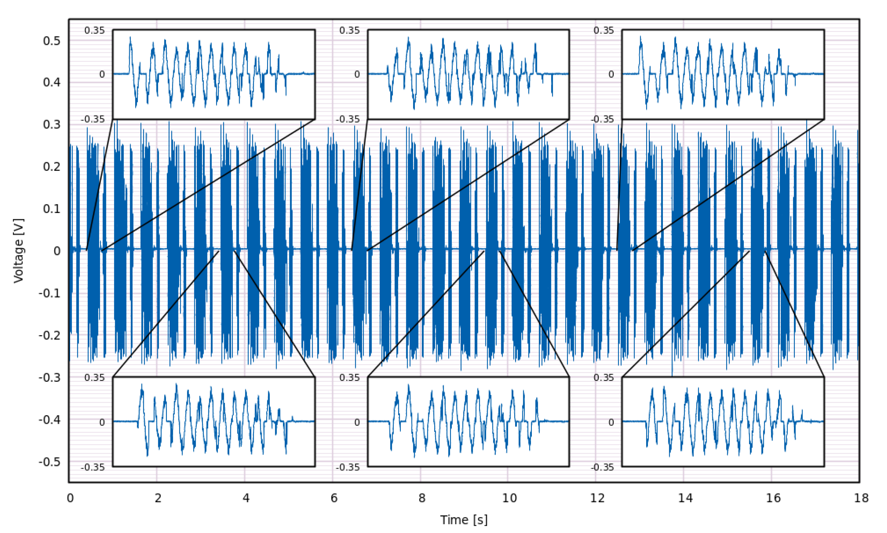
2.2.3. Piezoelectric Effect Measurements
3. Results and Discussion
Error Analysis
4. Conclusions
Author Contributions
Funding
Institutional Review Board Statement
Informed Consent Statement
Data Availability Statement
Conflicts of Interest
References
- 2021 State of the U.S. Semiconductor Industry; Technical Report; Semiconductor Industry Association: Washington, DC, USA, 2021.
- Is It Time for a Revolution? Available online: https://www.vlsiresearch.com/ (accessed on 17 January 2022).
- IRDS 2021: Executive Summary. Technical Report. 2021. Available online: https://irds.ieee.org/editions/2021 (accessed on 21 September 2022).
- Al-Fuqaha, A.; Guizani, M.; Mohammadi, M.; Aledhari, M.; Ayyash, M. Internet of Things: A Survey on Enabling Technologies, Protocols, and Applications. IEEE Commun. Surv. Tutor. 2015, 17, 2347–2376. [Google Scholar] [CrossRef]
- Farber, D. Counting the Internet of Things in Real Time. Available online: https://www.cnet.com/science/counting-the-internet-of-things-in-real-time/ (accessed on 23 June 2022).
- Columbus, L. Roundup of Internet of Things Forecasts and Market Estimates. 2016. Available online: https://www.forbes.com/sites/louiscolumbus/2016/11/27/roundup-of-internet-of-things-forecasts-and-market-estimates-2016/ (accessed on 23 June 2022).
- Press, G. Internet of Things by the Numbers: Market Estimates and Forecasts. Available online: http://www.forbes.com/sites/gilpress/2014/08/22/internet-of-things-by-the-numbers-market-estimates-and-forecasts (accessed on 23 June 2022).
- IoT Platforms Market Report 2018–2023. Technical Report. 2018. Available online: https://iot-analytics.com/product/iot-platforms-market-report-2018-23/ (accessed on 21 September 2022).
- An Introduction to Internet of Things (IoT) and Lifecycle Management—Interoperability Architecture and Standards. Available online: http://www.opengroup.org/iot/iotwp/p3.htm (accessed on 20 June 2022).
- The 2022 McClean Report, a Complete Analysis and Forecast of the Semiconductor Industry. Technical Report; IC Insights Inc.: Scottsdale, AZ, USA, 2021.
- World Population Prospects 2019. Technical Report; Department of Economic and Social Affairs, Population Division, United Nations: New York, NY, USA, 2019. Available online: https://www.un.org/development/desa/publications/world-population-prospects-2019-highlights.html (accessed on 21 September 2022).
- Briand, D.; Yeatman, E.; Roundy, S.; Brand, O.; Fedder, G.; Hierold, C.; Korvink, J.; Tabata, O. Micro Energy Harvesting; Advanced Micro and Nanosystems; Wiley: Hoboken, NJ, USA, 2015. [Google Scholar]
- Berndt, E.R.; Rappaport, N.J. Price and Quality of Desktop and Mobile Personal Computers: A Quarter-Century Historical Overview. Am. Econ. Rev. 2001, 91, 268–273. [Google Scholar] [CrossRef]
- Schwierz, F. Graphene transistors. Nat. Nanotechnol. 2010, 5, 487–496. [Google Scholar] [CrossRef]
- International Technology Roadmap for Semiconductors 2001 (Updated 2002); Technical Report; International Roadmap Commitee: Geneva, Switzerland, 2002.
- Richards, M.; Shaw, G. Chips, Architectures and Algorithms: Reflections on the Exponential Growth of Digital Signal Processing Capability. 2004. Available online: https://wiki.santafe.edu/images/4/4b/RichardsShaw.pdf (accessed on 21 September 2022).
- Caliò, R.; Rongala, U.; Camboni, D.; Milazzo, M.; Stefanini, C.; de Petris, G.; Oddo, C. Piezoelectric Energy Harvesting Solutions. Sensors 2014, 14, 4755–4790. [Google Scholar] [CrossRef] [PubMed]
- Haras, M.; Skotnicki, T. Thermoelectricity for IoT—A review. Nano Energy 2018, 54, 461–476. [Google Scholar] [CrossRef]
- Vullers, R.; van Schaijk, R.; Doms, I.; Hoof, C.V.; Mertens, R. Micropower energy harvesting. Solid-State Electron. 2009, 53, 684–693. [Google Scholar] [CrossRef]
- Matiko, J.W.; Grabham, N.J.; Beeby, S.P.; Tudor, M.J. Review of the application of energy harvesting in buildings. Meas. Sci. Technol. 2013, 25, 012002. [Google Scholar] [CrossRef]
- IEC 61215-1-1; Terrestrial Photovoltaic (PV) Modules—Design Qualification and Type Approval—Part 1: Test Requirements. International Electrotechnical Commission (IEC): Geneva, Switzerland, 2016.
- 90.1-2016; Energy Standard for Buildings Except Low-Rise Residential Buildings. ANSI/ASHRAE/IES: Washington, DC, USA, 2016.
- Sherrit, S.; Lee, H.J.; Walkemeyer, P.; Winn, T.; Tosi, L.P.; Colonius, T. Fluid flow nozzle energy harvesters. In Proceedings of the Sensors and Smart Structures Technologies for Civil, Mechanical, and Aerospace Systems, San Diego, CA, USA, 9–12 March 2015; Lynch, J.P., Ed.; SPIE: Bellingham, WA, USA, 2015. [Google Scholar] [CrossRef]
- Lee, H.; Sherrit, S.; Tosi, L.; Walkemeyer, P.; Colonius, T. Piezoelectric Energy Harvesting in Internal Fluid Flow. Sensors 2015, 15, 26039–26062. [Google Scholar] [CrossRef]
- Visser, H.J.; Reniers, A.C.F.; Theeuwes, J.A.C. Ambient RF Energy Scavenging: GSM and WLAN Power Density Measurements. In Proceedings of the 2008 38th IEEE European Microwave Conference, Amsterdam, The Netherlands, 27–31 October 2008. [Google Scholar] [CrossRef]
- Duangsuwan, S.; Leukachorn, T.; Chinsawatpan, S.; Promwong, S. Experimental study for polarimetric measurement of RFID transfer function with in an indoor environment. In Proceedings of the 2009 IEEE 9th Malaysia International Conference on Communications (MICC), Kuala Lumpur, Malaysia, 15–17 December 2009. [Google Scholar] [CrossRef]
- Lo, H.W.; Tai, Y.C. Parylene-based electret power generators. J. Micromech. Microeng. 2008, 18, 104006. [Google Scholar] [CrossRef]
- Despesse, G.; Jager, T.; Jean-Jacques, C.; Léger, J.M.; Vassilev, A.; Basrour, S.; Charlot, B. Fabrication and characterization of high damping electrostatic micro devices for vibration energy scavenging. In Proceedings of the Design, Test, Integration and Packaging of MEMS and MOEMS (DTIP MEMS/MOEMS), Montpellier, France, 27–30 April 2015; pp. 386–390. [Google Scholar] [CrossRef]
- Markiewicz, M.; Wielgosz, M.; Bochenski, M.; Tabaczynski, W.; Konieczny, T.; Kowalczyk, L. Predictive Maintenance of Induction Motors Using Ultra-Low Power Wireless Sensors and Compressed Recurrent Neural Networks. IEEE Access 2019, 7, 178891–178902. [Google Scholar] [CrossRef]
- Markiewicz, M.; Dziurdzia, P.; Konieczny, T.; Skomorowski, M.; Kowalczyk, L.; Skotnicki, T.; Urard, P. Software Controlled Low Cost Thermoelectric Energy Harvester for Ultra-Low Power Wireless Sensor Nodes. IEEE Access 2020, 8, 38920–38930. [Google Scholar] [CrossRef]
- Schils, R. Pierre Curie. In How James Watt Invented the Copier: Forgotten Inventions of Our Great Scientists; Springer: New York, NY, USA, 2011. [Google Scholar]
- Katzir, S. Who knew piezoelectricity? Rutherford and Langevin on submarine detection and the invention of sonar. Notes Rec. R. Soc. 2012, 66, 141–157. [Google Scholar] [CrossRef]
- Baltaci, V.; Ayvaz, Ö.Ü.; Ünsal, E.; Aktaş, Y.; Baltacı, A.; Turhan, F.; Özcan, S.; Sönmezer, M. The effectiveness of intracytoplasmic sperm injection combined with piezoelectric stimulation in infertile couples with total fertilization failure. Fertil. Steril. 2010, 94, 900–904. [Google Scholar] [CrossRef]
- Manbachi, A.; Cobbold, R.S.C. Development and Application of Piezoelectric Materials for Ultrasound Generation and Detection. Ultrasound 2011, 19, 187–196. [Google Scholar] [CrossRef]
- Gautsch, S.; Staufer, U.; Akiyama, T.; Hidber, H.R.; Tonin, A.; Howald, L.; Müller, D.; Niedermann, P.; de Rooij, N.F. Miniaturized atomic force microscope for planetary exploration. In Proceedings of the 9th European Space Mechanisms and Tribology Symposium, Liège, Belgium, 19–21 September 2001; Volume 480, pp. 11–16. [Google Scholar]
- Nandi, A.; Neogy, S.; Bhaduri, S.; Irretier, H. Vibration Attenuation by a Combination of a Piezoelectric Stack and a Permanent Magnet. Shock Vib. 2012, 19, 719–734. [Google Scholar] [CrossRef][Green Version]
- Inaba, R.; Tokushima, A.; Kawasaki, O.; Ise, Y.; Yoneno, H. Piezoelectric Ultrasonic Motor. In Proceedings of the IEEE 1987 Ultrasonics Symposium, Sheraton Denver Tech Center, Denver Colorado, CO, USA, 14–16 October 1987. [Google Scholar] [CrossRef]
- Piezoelectric Energy Harvesting; John Wiley & Sons, Ltd.: Hoboken, NJ, USA, 2011. [CrossRef]
- Harb, A. Energy harvesting: State-of-the-art. Renew. Energy 2011, 36, 2641–2654. [Google Scholar] [CrossRef]
- Briscoe, J.; Dunn, S. Nanostructured Piezoelectric Energy Harvesters; SpringerBriefs in Materials; Springer International Publishing: Berlin/Heidelberg, Germany, 2014. [Google Scholar]
- Li, Z.; Wang, Z.L. Air/Liquid-Pressure and Heartbeat-Driven Flexible Fiber Nanogenerators as a Micro/Nano-Power Source or Diagnostic Sensor. Adv. Mater. 2010, 23, 84–89. [Google Scholar] [CrossRef]
- Sohn, H.; Kim, S.B. Development of dual PZT transducers for reference-free crack detection in thin plate structures. IEEE Trans. Ultrason. Ferroelectr. Freq. Control 2010, 57, 229–240. [Google Scholar] [CrossRef]
- Taylor, S.G.; Farinholt, K.; Choi, M.; Jeong, H.; Jang, J.; Park, G.; Lee, J.R.; Todd, M.D. Incipient crack detection in a composite wind turbine rotor blade. J. Intell. Mater. Syst. Struct. 2013, 25, 613–620. [Google Scholar] [CrossRef]
- Shenck, N.; Paradiso, J. Energy scavenging with shoe-mounted piezoelectrics. IEEE Micro 2001, 21, 30–42. [Google Scholar] [CrossRef]
- White, N.M.; Glynne-Jones, P.; Beeby, S.P. A novel thick-film piezoelectric micro-generator. Smart Mater. Struct. 2001, 10, 850–852. [Google Scholar] [CrossRef]
- Roundy, S.; Wright, P.K.; Rabaey, J. A study of low level vibrations as a power source for wireless sensor nodes. Comput. Commun. 2003, 26, 1131–1144. [Google Scholar] [CrossRef]
- Lu, F.; Lee, H.P.; Lim, S.P. Modeling and analysis of micro piezoelectric power generators for micro-electromechanical-systems applications. Smart Mater. Struct. 2003, 13, 57–63. [Google Scholar] [CrossRef]
- Ng, T.H.; Liao, W.H. Sensitivity Analysis and Energy Harvesting for a Self-Powered Piezoelectric Sensor. J. Intell. Mater. Syst. Struct. 2005, 16, 785–797. [Google Scholar] [CrossRef]
- Jeon, Y.; Sood, R.; Jeong, J.H.; Kim, S.G. MEMS power generator with transverse mode thin film PZT. Sens. Actuators A Phys. 2005, 122, 16–22. [Google Scholar] [CrossRef]
- Roundy, S.; Leland, E.; Baker, J.; Carleton, E.; Reilly, E.; Lai, E.; Otis, B.; Rabaey, J.; Sundararajan, V.; Wright, P. Improving Power Output for Vibration-Based Energy Scavengers. IEEE Pervasive Comput. 2005, 4, 28–36. [Google Scholar] [CrossRef]
- Tanaka, H.; Ono, G.; Nagano, T.; Ohkubo, N. Electric power generation using piezoelectric resonator for power-free sensor node. In Proceedings of the IEEE 2005 Custom Integrated Circuits Conference, San Jose, CA, USA, 21 September 2005. [Google Scholar] [CrossRef]
- Elvin, N.G.; Lajnef, N.; Elvin, A.A. Feasibility of structural monitoring with vibration powered sensors. Smart Mater. Struct. 2006, 15, 977–986. [Google Scholar] [CrossRef]
- Fang, H.B.; Liu, J.Q.; Xu, Z.Y.; Dong, L.; Wang, L.; Chen, D.; Cai, B.C.; Liu, Y. Fabrication and performance of MEMS-based piezoelectric power generator for vibration energy harvesting. Microelectron. J. 2006, 37, 1280–1284. [Google Scholar] [CrossRef]
- Lefeuvre, E.; Badel, A.; Richard, C.; Petit, L.; Guyomar, D. Optimization of Piezoelectric Electrical Generators Powered by Random Vibrations. arXiv 2007, arXiv:0711.3309. [Google Scholar] [CrossRef]
- Kok, S.L.; White, N.M.; Harris, N.R. A novel piezoelectric thick-film free-standing cantilever energy harvester. In Proceedings of the Eurosensors XXII, Dresden, Germany, 6–10 September 2008; Available online: https://www.sciencedirect.com/journal/sensors-and-actuators-a-physical/vol/156/issue/1 (accessed on 21 September 2022).
- Shen, D.; Park, J.H.; Ajitsaria, J.; Choe, S.Y.; Wikle, H.C.; Kim, D.J. The design, fabrication and evaluation of a MEMS PZT cantilever with an integrated Si proof mass for vibration energy harvesting. J. Micromech. Microeng. 2008, 18, 055017. [Google Scholar] [CrossRef]
- Zhu, D.; Beeby, S.; Tudor, J.; Harris, N. A Self Powered Tag for Wireless Structure Health Monitoring in Aeronautical Applications. In Proceedings of the PowerMEMS 2009, Washington DC, USA, 1–4 December 2009; pp. 201–204. Available online: https://www.transducer-research-foundation.org/archive/powermems2009/ (accessed on 21 September 2022).
- Wu, Q.; Guo, H.; Sun, H.; Liu, X.; Sui, H.; Wang, F. Flexible piezoelectric energy harvesters with graphene oxide nanosheets and PZT-incorporated P(VDF-TrFE) matrix for mechanical energy harvesting. Ceram. Int. 2021, 47, 19614–19621. [Google Scholar] [CrossRef]
- Wang, Z.L.; Song, J. Piezoelectric Nanogenerators Based on Zinc Oxide Nanowire Arrays. Science 2006, 312, 242–246. [Google Scholar] [CrossRef] [PubMed]
- Wang, X.; Song, J.; Liu, J.; Wang, Z.L. Direct-Current Nanogenerator Driven by Ultrasonic Waves. Science 2007, 316, 102–105. [Google Scholar] [CrossRef] [PubMed]
- Qiu, Y.; Zhang, H.; Hu, L.; Yang, D.; Wang, L.; Wang, B.; Ji, J.; Liu, G.; Liu, X.; Lin, J.; et al. Flexible piezoelectric nanogenerators based on ZnO nanorods grown on common paper substrates. Nanoscale 2012, 4, 6568. [Google Scholar] [CrossRef]
- Briscoe, J.; Jalali, N.; Woolliams, P.; Stewart, M.; Weaver, P.M.; Cain, M.; Dunn, S. Measurement techniques for piezoelectric nanogenerators. Energy Environ. Sci. 2013, 6, 3035. [Google Scholar] [CrossRef]
- Al-Ruqeishi, M.S.; Mohiuddin, T.; Al-Habsi, B.; Al-Ruqeishi, F.; Al-Fahdi, A.; Al-Khusaibi, A. Piezoelectric nanogenerator based on ZnO nanorods. Arab. J. Chem. 2019, 12, 5173–5179. [Google Scholar] [CrossRef]
- Luo, G.; Luo, Y.; Zhang, Q.; Wang, S.; Wang, L.; Li, Z.; Zhao, L.; Teh, K.S.; Jiang, Z. The Radial Piezoelectric Response from Three-Dimensional Electrospun PVDF Micro Wall Structure. Materials 2020, 13, 1368. [Google Scholar] [CrossRef]
- Mariello, M.; Blad, T.; Mastronardi, V.; Madaro, F.; Guido, F.; Staufer, U.; Tolou, N.; De Vittorio, M. Flexible piezoelectric AlN transducers buckled through package-induced preloading for mechanical energy harvesting. Nano Energy 2021, 85, 105986. [Google Scholar] [CrossRef]
- Yao, M.; Li, L.; Wang, Y.; Yang, D.; Miao, L.; Wang, H.; Liu, M.; Ren, K.; Fan, H.; Hu, D. Mechanical Energy Harvesting and Specific Potential Distribution of a Flexible Piezoelectric Nanogenerator Based on 2-D BaTiO3-Oriented Polycrystals. ACS Sustain. Chem. Eng. 2022, 10, 3276–3287. [Google Scholar] [CrossRef]
- Jeong, S.J.; Kim, M.S.; Song, J.S.; Kyung Lee, H. Two-layered piezoelectric bender device for micro-power generator. Sens. Actuators A Phys. 2008, 148, 158–167. [Google Scholar] [CrossRef]
- Marzencki, M.; Ammar, Y.; Basrour, S. Integrated power harvesting system including a MEMS generator and a power management circuit. Sens. Actuators A Phys. 2008, 145–146, 363–370. [Google Scholar] [CrossRef]
- Ma, S.; Fang, G.; Li, C.; Sheng, S.; Fang, L.; Fu, Q.; Zhao, X.Z. Controllable Synthesis of Vertically Aligned ZnO Nanorod Arrays in Aqueous Solution. J. Nanosci. Nanotechnol. 2006, 6, 2062–2066. [Google Scholar] [CrossRef] [PubMed]
- Manekkathodi, A.; Lu, M.Y.; Wang, C.W.; Chen, L.J. Direct Growth of Aligned Zinc Oxide Nanorods on Paper Substrates for Low-Cost Flexible Electronics. Adv. Mater. 2010, 22, 4059–4063. [Google Scholar] [CrossRef] [PubMed]
- Garcia, A.J.L.; Jalabert, T.; Pusty, M.; Defoor, V.; Mescot, X.; Montanino, M.; Sico, G.; Loffredo, F.; Villani, F.; Nenna, G.; et al. Size and Semiconducting Effects on the Piezoelectric Performances of ZnO Nanowires Grown onto Gravure-Printed Seed Layers on Flexible Substrates. Nanoenergy Adv. 2022, 2, 197–209. [Google Scholar] [CrossRef]
- Abubakar, S.; Khalid, N.; Abd Rahman, S.F.; Tee, T.S.; Hamidon, M.N.; Talib, Z.A.; Sagadevan, S.; Paiman, S. Fabrication and characterization of nanostructured zinc oxide on printed microcontact electrode for piezoelectric applications. J. Mater. Res. Technol. 2020, 9, 15952–15961. [Google Scholar] [CrossRef]
- Dominguez, D.; Romo-Herrera, J.; Solorio, F.; Borbón-Núñez, H.; Landeros, M.; Díaz de León, J.; Contreras, E.; Contreras, O.; Olivas, A.; Reynoso-Soto, E.; et al. Low-temperature ozone treatment for carbon nanotube template removal: Improving the template-based ALD method. J. Nanoparticle Res. 2018, 20, 1–10. [Google Scholar] [CrossRef]
- Basnet, P.; Samanta, D.; Inakhunbi Chanu, T.; Mukherjee, J.; Chatterjee, S. Assessment of synthesis approaches for tuning the photocatalytic property of ZnO nanoparticles. SN Appl. Sci. 2019, 1, 1–13. [Google Scholar] [CrossRef]
- Seow, Z.L.S.; Wong, A.S.W.; Thavasi, V.; Jose, R.; Ramakrishna, S.; Ho, G.W. Controlled synthesis and application of ZnO nanoparticles, nanorods and nanospheres in dye-sensitized solar cells. Nanotechnology 2008, 20, 045604. [Google Scholar] [CrossRef]
- Ko, W.; Lee, S.; Myoung, N.; Hong, J. Solution processed vertically stacked ZnO sheet-like nanorod p–n homojunctions and their application as UV photodetectors. J. Mater. Chem. C 2016, 4, 142–149. [Google Scholar] [CrossRef]
- Keysight X-Series Oscilloscopes Data Sheet. Available online: https://www.keysight.com/us/en/assets/7018-02733/data-sheets/5990-6618.pdf (accessed on 21 September 2022).


| Sample ID | ALD Seed Layer | Reaction Solution Concentration (mM/dm) |
|---|---|---|
| A-100 | 200 nm ZnO (A) | 100 |
| A-30 | 200 nm ZnO (A) | 30 |
| B-75 | 20 nm AlO/200 nm ZnO (B) | 75 |
| B-50 | 20 nm AlO/200 nm ZnO (B) | 50 |
| Sample ID | 2 [deg] | D [nm] | ||
|---|---|---|---|---|
| (100) | (002) | (100) | (002) | |
| A-100 | 31.79 | 34.48 | 27.48 | 26.42 |
| A-30 | 31.86 | 34.43 | 27.49 | 26.43 |
| B-75 | 31.81 | 34.42 | 27.48 | 26.43 |
| B-50 | 31.89 | 34.51 | 20.61 | 19.82 |
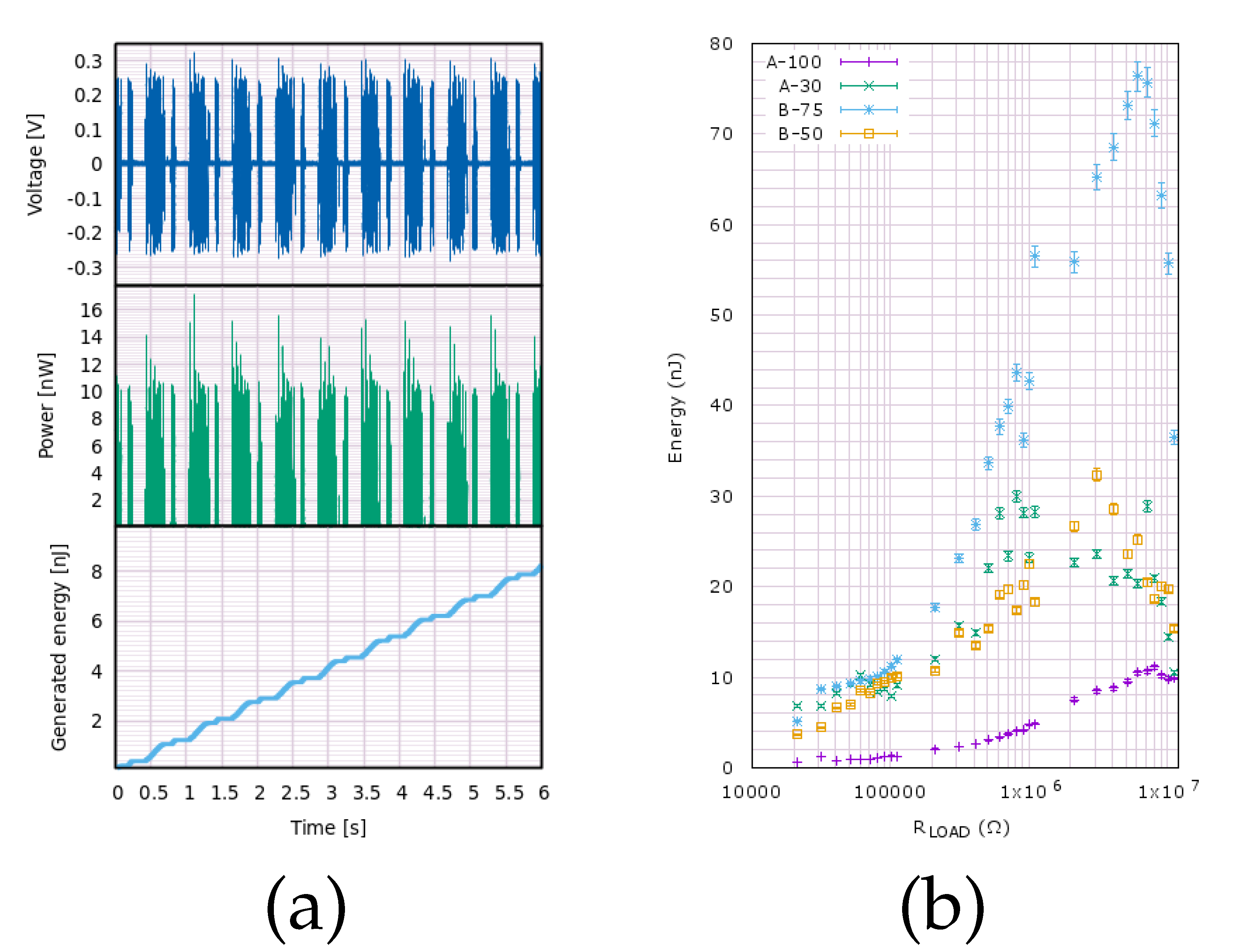
| Sample ID | Optimal Impedance | Max. Accumulated Energy | Max. Power | Max. Accumulated Energy Density | Max. Power Density |
|---|---|---|---|---|---|
| M | nJ | nW | J/cm | W/cm | |
| A-100 | 0.81 | 29.94 | 0.54 | 66.5 | 1.2 |
| A-30 | 8.11 | 11.18 | 0.20 | 24.8 | 0.4 |
| B-75 | 6.11 | 76.37 | 1.38 | 169.5 | 3.1 |
| B-50 | 3.11 | 32.36 | 0.58 | 71.8 | 1.3 |
Publisher’s Note: MDPI stays neutral with regard to jurisdictional claims in published maps and institutional affiliations. |
© 2022 by the authors. Licensee MDPI, Basel, Switzerland. This article is an open access article distributed under the terms and conditions of the Creative Commons Attribution (CC BY) license (https://creativecommons.org/licenses/by/4.0/).
Share and Cite
Wlazło, M.; Haras, M.; Kołodziej, G.; Szawcow, O.; Ostapko, J.; Andrysiewicz, W.; Kharytonau, D.S.; Skotnicki, T. Piezoelectric Response and Substrate Effect of ZnO Nanowires for Mechanical Energy Harvesting in Internet-of-Things Applications. Materials 2022, 15, 6767. https://doi.org/10.3390/ma15196767
Wlazło M, Haras M, Kołodziej G, Szawcow O, Ostapko J, Andrysiewicz W, Kharytonau DS, Skotnicki T. Piezoelectric Response and Substrate Effect of ZnO Nanowires for Mechanical Energy Harvesting in Internet-of-Things Applications. Materials. 2022; 15(19):6767. https://doi.org/10.3390/ma15196767
Chicago/Turabian StyleWlazło, Mateusz, Maciej Haras, Grzegorz Kołodziej, Oliwia Szawcow, Jakub Ostapko, Wojciech Andrysiewicz, Dzmitry S. Kharytonau, and Thomas Skotnicki. 2022. "Piezoelectric Response and Substrate Effect of ZnO Nanowires for Mechanical Energy Harvesting in Internet-of-Things Applications" Materials 15, no. 19: 6767. https://doi.org/10.3390/ma15196767
APA StyleWlazło, M., Haras, M., Kołodziej, G., Szawcow, O., Ostapko, J., Andrysiewicz, W., Kharytonau, D. S., & Skotnicki, T. (2022). Piezoelectric Response and Substrate Effect of ZnO Nanowires for Mechanical Energy Harvesting in Internet-of-Things Applications. Materials, 15(19), 6767. https://doi.org/10.3390/ma15196767