Next Article in Journal
Investigating the Microstructural and Mechanical Properties of Novel Ternary Reinforced AA7075 Hybrid Metal Matrix Composite
Previous Article in Journal
Microstructure and Mechanical Properties of Metal Foams Fabricated via Melt Foaming and Powder Metallurgy Technique: A Review
 
 
Retraction published on 2 April 2025, see Materials 2025, 18(7), 1623.
Article

RETRACTED: The Effect of 600 keV Ag Ion Irradiation on the Structural, Optical, and Photovoltaic Properties of MAPbBr3 Films for Perovksite Solar Cell Applications

1
Department of Physics, University of Lahore, Lahore 53700, Pakistan
2
Department of Physics, College of Sciences, Princess Nourah bint Abdulrahman University, P.O. Box 84428, Riyadh 11671, Saudi Arabia
3
Department of Chemistry, University of Lahore, Lahore 53700, Pakistan
*
Authors to whom correspondence should be addressed.
Materials 2022, 15(15), 5299; https://doi.org/10.3390/ma15155299
Submission received: 17 May 2022 / Revised: 14 July 2022 / Accepted: 20 July 2022 / Published: 1 August 2022 / Retracted: 2 April 2025

Abstract

:
A competitive new technology, organic metallic halide perovskite solar cells feature a wide working area, low manufacturing costs, a long lifespan, and a significant amount of large efficacy of power conversion (PCE). The spin-coating technique was utilized for the fabrication of pure CH3NH3PbBr3 (MAPbBr3) thin films, and these films are implanted with 600 keV silver (Ag) ions at fluency rate of 6 × 10¹⁴ and 4 × 10¹⁴ ions/cm2. XRD analysis confirmed the cubic structure of MAPbBr3. A high grain size was observed at the fluency rate of 4 × 10¹⁴ ions/cm2. The UV-Vis spectroscopic technique was used to calculate the optical properties such as the bandgap energy (Eg), refractive index (n), extinction coefficients (k), and dielectric constant. A direct Eg of 2.44 eV was measured for the pristine film sample, whereas 2.32 and 2.36 eV were measured for Ag ion-implanted films with a 4 × 10¹⁴ and 6 × 10¹⁴ ions/cm2 fluence rate, respectively. The solar cells of these films were fabricated. The Jsc was 6.69 mA/cm2, FF was 0.80, Voc was 1.1 V, and the efficiency was 5.87% for the pristine MAPbBr3-based cell. All of these parameters were improved by Ag ion implantation. The maximum values were observed at a fluency rate of 4 × 10¹⁴ ions/cm2, where the Voc was 1.13 V, FF was 0.75, Jsc was 8.18 mA/cm2, and the efficiency was 7.01%.

1. Introduction

In a very short amount of time, perovskites solar cells (PSCs) have attracted the attention of the photovoltaic industry by providing a solar-to-electric power conversion efficiency (PCE) rate greater than 23%. Currently, it is a potential candidate among commercially available solar cells, and nanomaterials play the main role in their efficiency [1,2,3,4,5,6]. Inorganic–organic hybrid perovskites of metals halides have a general formula: ABX3, where the A-site is composed of organic cations that usually consist of MA+ (CH3NH3+), Cs+, and FA+ [(NH2)2CH]+ ions, etc.; the B-site is composed of metallic cations, generally Pb2+, as other ions, such as Ge2+ and Sn2+, can easily oxidize to +4 states; the X-sites are composed of halide ions, e.g., Cl, Br, or I [7,8]. The common inorganic–organic perovskites compounds are FAPbI3 and MAPbI3. The MAPbI3-based PSCs have many benefits, like high charge extraction rate, and they can absorb a large range of visible light [9]. However, as it becomes crude in humid conditions, it cannot be commercialized on a large scale [10]. Thus, as an alternative to MAPbI3, MAPbBr3 is a promising candidate with a large bandgap of 2.2 eV that provides a high open-circuit voltage (≈1.2−1.5 V) [11,12]. Its excitonic length of diffusion is greater than 1.2 μm, which enables it with good charge transport ability within a device [13]. In addition, MAPbBr3, in comparison to pseudo-cubic MAPbI3, has a stable cubic phase that provides good stability in air or moisture conditions and low ionic mobility [14,15]. These favorable features of MAPbBr3 provide a large binding energy (76 MeV), high light absorption beyond the limit of 550 nm, and high efficiency [15,16].
Various studies have revealed that there are several fundamental properties on which the efficiency of perovskite solar cells (PSCs) depend. These properties include a high coefficient of absorption, a long lifetime of photogenerated species, and the tuneability of the band gap by changing the halide (i.e., bromide and iodide) fabrication of the perovskite precursor solution [17,18,19]. Due to the fact of these favorable features, ABX3-type hybrid perovskite compounds are capable of developing solar cells with PCE greater than 22%. However, some problematic issues still exist in PSCs such as instability in moisture and intensive light illumination as well as the presence of harmful Pb2+ ions. These serious issues provide the upper limit to their commercial development and higher efficiency [20,21]. Many approaches, such as substitutional changing of the A-site and X-sites with inorganic ions, have been utilized thus far, but remarkable results have not been achieved. To improve the stability, PSCs are optionally encapsulated by organic or inorganic materials [22] for the better dispersion of the microspheres of porous Si deposited on the surface of PSCs [23]; in addition, hydrophobic materials are also deposited to increase the stability and reduce the number of recombination centers [24]. Although these approaches are affected but cannot improve the stability of PSCs, another approach that is considered useful for improving the efficiency, thermal stability, and phase maturity of ABX3-type perovskites is the partial substitution of Pb+2 ions from B-sites with metallic ions [25,26,27].
This substitution of Pb2+ cations is an important and promising methods for increasing perovskite stability. Thus, replacing a toxic Pb+2 with a nontoxic element to improve the stability is a common task for scientists [28]. There is a wide range of cations with different atomic radii that may induce suitable changes in perovskites. However, as the formation of cations from the B-site requires a higher formation energy in comparison to A-sites and X-sites, they are more difficult to develop [24,29]. Thus, B-site doping is still a very sensitive issue [28,29]. Doping via a chemical method is a good technique for adding metal ions to a B-site, but this method is not effective, because chemical impurities can be added to the ABX3 structure, which reduces the efficiency and stability of the cell. Ion implantation is a good technique, compared to the chemical method, for the doping of metal ions in B-sites of perovskites. This involves the bombardment of the substrate with ions, accelerating to higher velocities. It requires a low-temperature process with no damage and selecting the quantity fabricated is also possible. It allows for controlling the precise dose and depth. These capabilities are not possible with doping [30,31]. In ion implantation, there are several controlling factors that make it versatile, e.g., the dopant fluency, dopant energy, and depth. Therefore, ion implantation can substitute metallic ions in the B-site of perovskite. Different metallic ions can be doped in the MAPbBr3 structure, but Ag is the most suitable for adding to B-sites due to the fact of its nontoxicity, abundance, cubic structure, and high stability. Ag has an atomic radius of 1.72 Å, which is comparable to the atomic radius of Pb, which is 1.8 Å [32]. Therefore, it will not change the structure of ABX3. During ion implantation, when Ag ions replace Pb ions in the B-site, it increases the electrical properties and stability of solar cells [33,34].
In this study, Ag ions were inserted in place of Pb via the ion implantation technique, which is a good doping technique compared to other chemical techniques. The Ag ions increased the stability and performance of the device. The detailed structural and optical properties of the Ag-implanted MAPbBr3 films are discussed, which have not previously been explored in other studies. It was observed that the Ag ions did not disturb the stable cubic phase of MAPbBr3. This indicated that the cells fabricated with Ag ions would be stable and have a long lifetime. Here, Ag ions affected the photovoltaic characteristics were investigated, and it was observed that the PSC fabricated at 4 × 10¹⁴ ions/cm2 had a high photovoltaic performance. From the literature survey, it was found that Ag ion implantation in MAPbI3 needed to be addressed.

2. Experimental Section

The precursors of MAPbBr3 perovskite, such as bromides of MA and Pb, were purchased from Sigma-Aldrich, UK. To prepare the 1 M solution of MAPbBr3 perovskite, dimethyl-sulfoxide and n-dimethyl-formamide were mixed together at a volumetric ratio of 7:3 and left for 12 h. Solution of Perovskite was coated onto FTO glass substrates using the spin-coating technique for 10 seconds at a speed of 4000 rpm. The FTO was bathed with deionized (DI) water first, then with isopropanol and ethanol before deposition. At fluence rates of 4 × 10¹⁴ and 6 × 10¹⁴ ions/cm2, two films received 600 keV Ag irradiation. After Ag ion implantation, the films were annealed in a furnace for 10 min at 100 °C.
The structural properties of the films were studied by X-ray diffractogram (D/MAX-2400), Vianna, Austria. UV-Vis spectroscopy (U-4100) was used to measure the optical characteristics, China.
The solar cells of these films were fabricated on TiO2/FTO/glass substrates. TiO2 film was coated onto the FTO/glass substates using a previously published technique [35]. For the preparation of hole transport material (HTM), 36 mL of TBP and 22 mL of a stock solution of 520 mg/mL lithium bis-trifluoromethyl sulfonyl-imide were combined to create solution (A). In solution (A), 72 mg of spiro-OMeTAD was added and stirred, and a solution formed called solution (B). Chlorobenzene (1 mL) was dissolved in solution (B) to prepare a final solution. The volatilized gold layer, with an 80 nm thickness, was coated on the top of the electrode. The gold coating increased the wettability of the photo-active layer, increased the performance time, and established a better contact of device with the external source [36]. The cell’s active area measured 0.16 cm2.
The efficacy of cells was recorded by a solar simulator (AM 1.5G illumination at 100 mWcm−2 using a source meter from Keithley 2450). The stepwise deposition of different layers is shown in Figure 1.

3. Results and Discussion
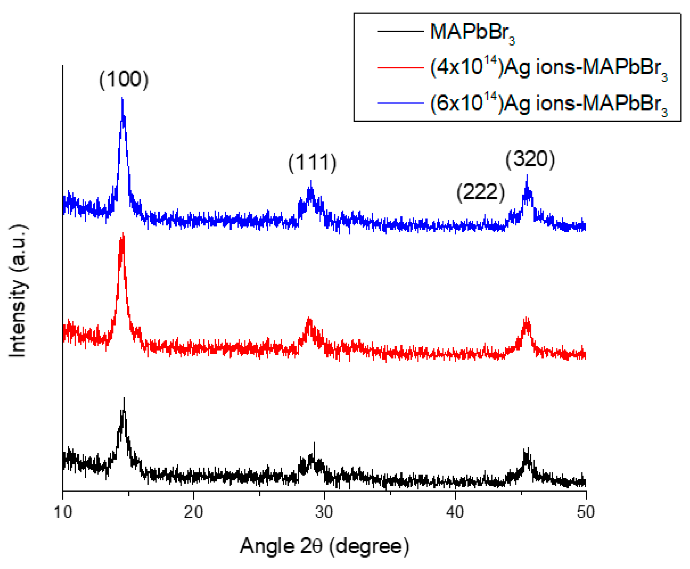
3.1. XRD Analysis

An XRD graph of the pristine and Ag-implanted MAPbBr3 films is shown in Figure 2. In the pristine MAPbBr3, four peaks appeared at 2θ values of 14.66°, 29.16°, 42.20°, and 45.54°, having a plane orientation (100), (111), (222), and (320), respectively. All peaks confirmed the cubic perovskite structure of MAPbBr3, which has also been reported in the literature [37]. For the Ag-implanted MAPbBr3 at the fluency rate of 4 × 10 14 ions/cm2, the four peaks were observed at 2θ values of 14.59° (100), 28.77° (111), 42.16° (222), and 45.48° (320). Here, the peaks shifted, and the intensity of the peaks increased, which indicates that the crystallinity of the film increased. At the fluency rate of 6 × 10 14 Ag ions/cm2, the four peaks were located at 2θ values of 14.50° (100), 28.72° (111), 42.20° (222), and 45.44° (320). All peaks were shifted toward lower 2θ angles, and no additional peaks related to AgBr, AgPb, etc., were observed, which attests to the stability of the phase and the correct replacement of Ag ions in the MAPbBr3 host [38]. Additionally, it indicated the absence of stresses in the unit cell [39].

3.1.1. Grain Size (D) and Dislocation Line Density ( δ )

δ and D of highly intense (100) peaks were measured using the following formulas [40,41]:
D = 0.9 λ β cos θ
δ = 1 D 2
Here, λ is the wavelength; β and θ are the FWHM and Brag’s angle, respectively [42].
For pure MAPbBr3 films, D was 19 nm and δ was 3.52 × 10 15   m 2 as shown in Figure 3. For the Ag-implanted MAPbBr3, D and δ at the fluency rate of 4 × 10 14 ions/cm2 were 26 nm and 3.44 × 10 15   m 2 , respectively. The high value of the grain size refers to the proper substitution of Ag ions in the ABX3 structure due to the fact that the crystallinity of the film was high, as a high peak intensity was observed at this fluency rate in the film. The low value of δ indicated that the scattering of electrons was low due to the small grain boundaries. At a rate of 6 × 10 14 ions/cm2, D and δ were 22 nm and 4.42 × 10 15   m 2 , respectively. The high value of Ag ions indicates that they did not occupy the vacant Pb sites, as they remained on the surface of MAPbBr3 due to the fact of small vacant sites. Therefore, D was reduced because of bonding between Ag ions and the inner atoms of MAPbBr3 [43]. These results match the previously published literature, where D decreased with a high amount of doping of divalent/trivalent ions in a MAPbBr3 structure [44,45]. The high concentration of Ag ions forms a network with MAPbBr3, which will increase and decrease the recombination rate [46].

3.1.2. d-Spacing

Figure 4 shows the d-spacing of the pure and Ag ion-implanted MAPbBr3 films. The d-spacing was measured by Bragg’s Law [5,30].
d = n λ 2 sin θ
where n is order of diffraction.
The values of d-spacing for the (100) peak of the pristine and the 4 × 10 14 ions/cm2 and 6 × 10 14 ions/cm2 Ag ion-implanted MAPbBr3 films were 6.11 Å, 6.1 Å, and 6.04 Å, respectively. The measured values showed a cubic crystal behavior according to file number PDF#21–1272 [5,30]. A slight decrease in the d-spacing values was observed by ion implantation. The decrease in d-spacing was due to the fact that Ag has a smaller ionic size. The slightly low value of the d-spacing shows that strong bonding was present between atoms and atoms and between planes and planes in the film’s structure [31]. This will benefit the enhancement of the stability of the structure.

3.1.3. Lattice Parameters and Volume

The lattice parameters and volume of a unit cell of pure and Ag-irradiated MAPbBr3 were calculated using Equations (5) and (6) and are shown in Figure 5.
a = dhkl(h2 + k2 + l2)1/2
V = a3
Here, hkl is the Miller indices of the most intense peak (i.e., (100)); V and a are the volume and lattice parameters of the unit cell.
The a and V of pure and 4 × 10 14 ions/cm2 and 6 × 10 14 ions/cm2 Ag ion-implanted MAPbBr3 films were 6.11 × 10 10 and 2.28 × 10 28   m 3 , 6.10 × 10 10 and 2.20 × 10 28   m 3 , and 6.04 × 10 10 and 2.27 × 10 28   m 3 , respectively. A decreasing trend in a and V was observed as shown in Figure 5 and Table 1. As Ag has a smaller radius than Pb, the volume of the unit cell therefore decreased. This was also confirmed from the XRD graph, where the peaks were shifted toward a small angle. Due to the fact of this decrease in volume, atoms become too close to each other, and the binding energy and number of electrons per unit volume increase. These large electrons will increase the electrical properties of the film, resulting in the improvement of the efficiency of the films.

3.2. Optical Properties

For solar cells, a material’s optical characteristics are crucial. This section explains optical parameters including refractive index, band gap energy, optical dielectrical constants, and extinction coefficient.

3.2.1. Energy Band Gap

The response of the material under the irradiation of light highly relies on its band gap and the energy of the incident photon. The photons energize the electrons with energy () more than bandgap energy (Eg) upon impact with the material; then, they absorb this energy due to the interband transition of the electrons. This phenomenon helps in analyzing the absorption edges of the material. To determine the bandgap of the material, these absorption edges were used with Tauc’s formula [47,48].
( α h υ ) 2 = B ( h υ E g )
Here, α is coefficient of absorption; B is a constant; is the energy of the incident photon; Eg is the bandgap of the material [49]. The value of Eg was measured from Figure 6 by extrapolating it at zero-ordinate. The Eg of pure MAPbBr3 was calculated as 2.44 eV. When Ag was irradiated onto MAPbBr3 film at rate of 4 × 10¹⁴ ions/cm2, its Eg decreased to 2.32 eV. The exchange interaction of sp-d between the localized “d” electrons of the transitions metals ions at the cation site and band electrons was used to explain this decrease in Eg [50]. The 5s and p orbitals of Ag and halogen respectively are contributed to the valence band’s upper edge, and only the 5p orbital of Ag do so for the conduction band’s lower edge. The level of energy of the 6p empty orbitals of Pb2+ is lower than the 5p empty orbitals of Ag2+ when the affinity of electrons and redox potential of Pb2+ are taking into account [51]. As a result, the conduction band’s bottom shifts downward with rising Ag content. This decrease in Eg is because of an increase in the ‘D’ of the film [52]. At a fluency rate 6 × 10¹⁴ ions/cm2, Eg was increased to 2.36 eV. This increase in Eg was due to the decrease in the grain size of the film. An Eg of 2.32 eV is most suitable for harvesting energy in the visible range [53]. The same results were also reported by Albert et al., where they doped the polycrystalline MAPbBr3 film with N2 and observed a low recombination rate [54].

3.2.2. Extinction Coefficient (k) and Refractive Index (n)

The n is a very important factor in photo-electronic and solar cell devices, because it analyzes the opto-electrical characteristics of the material. The refractive index can be measured by Lorentz classical theory [45,55].
n = 1 + ( A E g + B ) 2
Here, the constants are B and A having values are 3.4 eV and 13.6 eV, respectively. The measured refractive indexes for pure and 4 × 10 14 and 6 × 10 14 ions/cm2 Ag ion-implanted MAPbBr3 were 2.46, 2.60, and 2.56, respectively. The film implanted with at 4 × 10 14 ions/cm2 had a high refractive index, which is suggested good for the appications of solar cell. The high value of n increases the polarizability of the film [56,57]. Due to the high value of n, more light will scatter, leading to more energetic electrons being emitted. These high numbers of electrons will increase the current density of solar cells, which will cause the efficiency of the cell to increase.
The extinction coefficient k is calculated by [58]:
k = n Δ χ γ
Here, γ = −0.32 is the constant, and “∆χ∗” is the electronegativity [59]. The measured k for pure and 4 × 10 14 and 6 × 10 14 ions/cm2 Ag ion-implanted MAPbBr3 were 2.16, 2.23, and 2.21, respectively, as shown in Figure 7. When Ag ions were implanted, k increased, as it has a direct relation with n. The high value of k was observed at a fluency rate of 4 × 10¹⁴ ions/cm−2.

3.2.3. Dielectric Constants (εr, εi)

The optical constants of dielectric are related to a material’s inherent qualities. The dielectric constants are made up of real and imaginary elements. The real components refer to the light’s speed in the materials. The imaginary component concerns the dielectric material, which, as a result of dipole motion, absorbs energy from an electric field. The ratio between εr and εi determines the loss factor [60]. Additionally connected to dielectric constants are k and n. The relationship between polarizability and dielectric constant for every solid substance is proportional. The optical bandgap and position density are connected. Therefore, It is crucial to determine the dielectric constants precisely [61].
ε = εr + i εi
The εr and εi are determined using the given relations [62]:
εr = n2 − k2
εi = 2nk
Photon energy is necessary for both εr and εi. The εr of the pure and 4 × 10 14 ions/cm2 Ag ion-implanted MAPbBr3 films had higher values, and the value for the 6 × 10 14 ions/cm2 Ag ion-implanted MAPbBr3 film decreased. The εi allows for a comparison between the same refractive index values, as is shown in Table 2. εr and εi are at the maximum at a 4 × 10 14 ions/cm2 Ag ion concentration.

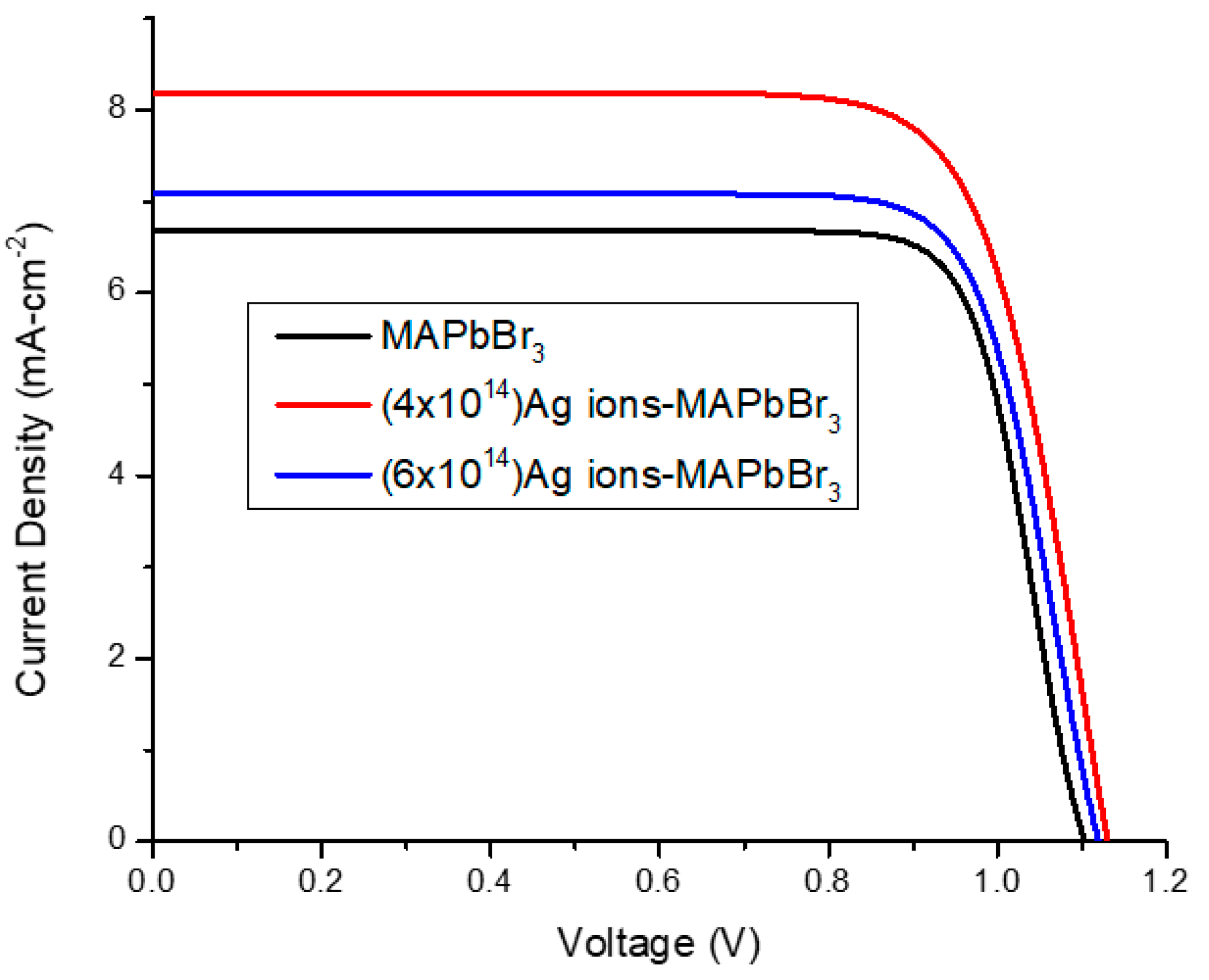
3.3. J-V Measurement

The conduction band (CB) and valence band (VB) edges for the construction of PSCs are very important. The CB edge of the perovskite film should be greater than the CB of the electron transport layer, and the VB edge of perovskite film should be greater than the VB of the hole-transport layer. The method for calculating the CB and VB edges of MAPbBr3 film is explained below [63]. The formula for MAPbBr3 is CH3NH3PbBr3, which includes one carbon, six hydrogen, one nitrogen, one lead, and three bromide atoms.
Electron affinity for C = EEA = 1.26/96.48 = 1.26 eV;
First ionization energy for C = Eion = 1086.5/96.48 = 11.26 eV;
Average energy = XC = 1/2(EEA + Eion) = 1/2(1.26 + 11.26) = 6.26 eV.
Similarly, the average energies of H, N, Pb, and Br were calculated, which were 6.42, 7.27, 3.52, and 4.24 eV, respectively.
Now:
XCH3NH3PbBr3 = [6.26 × (6.42)6 × 7.27 × 3.52 × (4.24)3]1/12;
XCH3NH3PbBr3 = 2.56 eV;
Ec = 2.56 − 4.5 − Eg/2 = −3.2 eV;
Ev = Ec − Eg = −5.60 eV.
These values matched well with the available literature [64].
Figure 8 shows the energy band structure diagram of a Ag/Spiro-OMeTAD/MAPbBr3/TiO2/FTO/glass solar cell. Light at a suitable frequency falls on the MAPbBr3, and then electron–hole pairs are generated. The electron accelerates toward the CB of TiO2, which is close to the CB of MAPbBr3, and the hole moves toward the VB of spiro-OMeTAD, the VB level of which is just above the VB level of MAPbBr3. In this way, the electron moves towards the circuit causing the current to flow through the solar cell.
Figure 9 shows the J-V curve of pure and Ag-irradiated MAPbBr3 solar cells. These curves were used to calculate the photovoltaic parameters of the pure and Ag-irradiated MAPbBr3-based solar cells such as the short circuit current density (Jsc), conversion efficiency (η), open-circuit voltage (Voc), and fill factor (FF), as summarized in Table 3. To determine the power conversion efficiency, the Equation (12) was used [65].
η = F F × V O C × J S C P i n
Here, Pin stands for the input power of the incident light. The FF is computed as follows [66]:
F F = I max × V max J S C × V O C
Here, Imax and Vmax are the maximum current and maximum voltage, respectively.
For the pure MAPbBr3-based solar cells, the calculated Jsc, Voc, FF, and efficiency were measured as 6.69 mAcm−2, 1.1 V, 0.79, and 5.86%, respectively.
When silver (Ag) ions were irradiated on the film of a sample MAPbBr3 at a fluency rate of 4 × 10 14 , the photovoltaic parameters (i.e., Jsc, Voc, and FF) improved and the efficiency increased from 5.86 to 7.01%. The improvement in photovoltaic parameters was caused by the irradiation of Ag ions, because they not only facilitate the growth of grains but also reduce the size of grain boundaries [48,67]. The grain boundary resistance is decreased by enhancing the charge carriers, which improves the Jsc [68,69]. In addition, Ag is a noble metal, and it increased the number of free electrons in the MAPbBr3 films, causing Jsc and FF to increase [70]. A high FF means that the recombination rate was reduced; therefore, the efficiency of the solar cell increases. Ag has free electrons, and a small amount of energy will cause the loss of these electrons from Ag and improve the concentration of free electrons in MAPbBr3; therefore, the Jsc is improved [71].
Additionally, it is observed from Figure 8 that the CB edge of MAPbBr3 came close to the CB of TiO2 by Ag ion implantation. Therefore, the electrons easily transferred from the CB of MAPbBr3 to the CB of TiO2; hence, Jsc increased leading to the increase the cell’s efficacy.
At a high flounce rate of 6 × 10¹⁴ ions/cm2, the efficiency of the cell decreased from 7.01% to 6.21% by decreasing Jsc and FF. The high value of Ag ions could not fit in the structure of MAPbBr3 as explained by XRD. The grain size decreased leading to the increase in the resistivity. Therefore, the recombination rate increased, which reduced the injection efficiency of the electrons from the CB of MAPbBr3 to the CB of TiO2; hence, Jsc was reduced and, finally, the efficiency was reduced, which has promising applications for harvesting solar light [72,73].

4. Conclusions

Perovskite solar cells of pure and 4 × 10 14 and 6 × 10 14 ions/cm2 Ag ion-implanted MAPbBr3 films were successfully prepared. All films had a stable cubic phase, and the film implanted with 4 × 10 14 ions/cm2 Ag ions had a large grain size, low bandgap (Eg), and high refractive index (n) according to XRD and UV-Vis analyses. These properties make it a good material for the fabrication of solar cells. Solar cells using these films were prepared. All solar cells showed good efficiency, but the cells formed with 4 × 10 14 ions/cm2 Ag ions implanted in the MAPbBr3 film showed high Voc (1.13 V), Jsc (8.18 mA-cm−2), FF (0.75), and efficiency (7.01%). This high efficiency was due to the high grain size and low band gap energy.

Author Contributions

Conceptualization, M.I.K., H.A.; methodology and investigation, S.H., M.I. (Muhammad Irfan); project administration and funding acquisition, N.A.; formal analysis, N.A., A.H.A.; resources, A.H.A., M.M.A.; data curation, M.I.K.; Methodology; writing—original draft preparation, I.-u.-H., M.I. (Muhammad Irfan); formal analysis, Writing—review & editing, M.I. (Munawar Iqbal), M.M.A. All authors have read and agreed to the published version of the manuscript.

Funding

This work was funded by the Deanship of Scientific Research at Princess Nourah bint Abdulrahman University through the Research Groups Program (grant no. RGP-1443-0039).

Institutional Review Board Statement

Not applicable.

Informed Consent Statement

Not applicable.

Data Availability Statement

Not applicable.

Acknowledgments

This work was funded by the Deanship of Scientific Research at Princess Nourah bint Abdulrahman University through the Research Groups Program (grant no. RGP-1443-0039).

Conflicts of Interest

The authors declare no conflict of interest.

References

  1. Amjad, M.; Khan, M.I.; Alwadai, N.; Irfan, M.; Albalawi, H.; Almuqrin, A.H.; Almoneef, M.M.; Iqbal, M. Photovoltaic Properties of ZnO Films Co-Doped with Mn and La to Enhance Solar Cell Efficiency. Nanomaterials 2022, 12, 1057. [Google Scholar] [CrossRef] [PubMed]
  2. Khan, M.I.; Mukhtar, A.; Alwadai, N.; Irfan, M.; Haq, I.-u.; Albalawi, H.; Almuqrin, A.H.; Almoneef, M.M.; Iqbal, M. Improving the Structural, Optical and Photovoltaic Properties of Sb-and Bi-Co-Doped MAPbBr3 Perovskite Solar Cell. Coatings 2022, 12, 386. [Google Scholar] [CrossRef]
  3. Lee, S.; Joung, Y.-H.; Yoon, Y.-K.; Choi, W. Preparation of a ZnO Nanostructure as the Anode Material Using RF Magnetron Sputtering System. Nanomaterials 2022, 12, 215. [Google Scholar] [CrossRef]
  4. Kolenčík, M.; Ernst, D.; Komár, M.; Urík, M.; Šebesta, M.; Ďurišová, Ľ.; Bujdoš, M.; Černý, I.; Chlpík, J.; Juriga, M.; et al. Effects of Foliar Application of ZnO Nanoparticles on Lentil Production, Stress Level and Nutritional Seed Quality under Field Conditions. Nanomaterials 2022, 12, 310. [Google Scholar] [CrossRef] [PubMed]
  5. Grancini, G.; Nazeeruddin, M.K. Dimensional tailoring of hybrid perovskites for photovoltaics. Nat. Rev. Mater. 2019, 4, 4–22. [Google Scholar] [CrossRef]
  6. Green, M.A.; Ho-Baillie, A. Perovskite solar cells: The birth of a new era in photovoltaics. ACS Energy Lett. 2017, 2, 822–830. [Google Scholar] [CrossRef]
  7. Correa-Baena, J.-P.; Saliba, M.; Buonassisi, T.; Grätzel, M.; Abate, A.; Tress, W.; Hagfeldt, A. Promises and challenges of perovskite solar cells. Science 2017, 358, 739–744. [Google Scholar] [CrossRef] [PubMed]
  8. Snaith, H.J. Perovskites: The emergence of a new era for low-cost, high-efficiency solar cells. J. Phys. Chem. Lett. 2013, 4, 3623–3630. [Google Scholar] [CrossRef]
  9. Xing, G.; Mathews, N.; Sun, S.; Lim, S.S.; Lam, Y.M.; Grätzel, M.; Mhaisalkar, S.; Sum, T.C. Long-range balanced electron-and hole-transport lengths in organic-inorganic CH3NH3PbI3. Science 2013, 342, 344–347. [Google Scholar] [CrossRef] [PubMed]
  10. Han, Y.; Meyer, S.; Dkhissi, Y.; Weber, K.; Pringle, J.M.; Bach, U.; Spiccia, L.; Cheng, Y.-B. Degradation observations of encapsulated planar CH 3 NH 3 PbI 3 perovskite solar cells at high temperatures and humidity. J. Mater. Chem. A 2015, 3, 8139–8147. [Google Scholar] [CrossRef]
  11. Zheng, X.; Chen, B.; Wu, C.; Priya, S. Room temperature fabrication of CH3NH3PbBr3 by anti-solvent assisted crystallization approach for perovskite solar cells with fast response and small J–V hysteresis. Nano Energy 2015, 17, 269–278. [Google Scholar] [CrossRef]
  12. Arora, N.; Orlandi, S.; Dar, M.I.; Aghazada, S.; Jacopin, G.; Cavazzini, M.; Mosconi, E.; Gratia, P.; De Angelis, F.; Pozzi, G.; et al. High open-circuit voltage: Fabrication of formamidinium lead bromide perovskite solar cells using fluorene–dithiophene derivatives as hole-transporting materials. ACS Energy Lett. 2016, 1, 107–112. [Google Scholar] [CrossRef]
  13. Kedem, N.; Brenner, T.M.; Kulbak, M.; Schaefer, N.; Levcenko, S.; Levine, I.; Abou-Ras, D.; Hodes, G.; Cahen, D. Light-induced increase of electron diffusion length in ap–n junction type CH3NH3PbBr3 perovskite solar cell. J. Phys. Chem. Lett. 2015, 6, 2469–2476. [Google Scholar] [CrossRef] [PubMed]
  14. Sheng, R.; Ho-Baillie, A.; Huang, S.; Chen, S.; Wen, X.; Hao, X.; Green, M.A. Methylammonium lead bromide perovskite-based solar cells by vapor-assisted deposition. J. Phys. Chem. C 2015, 119, 3545–3549. [Google Scholar] [CrossRef]
  15. Talbert, E.M.; Zarick, H.F.; Orfield, N.J.; Li, W.; Erwin, W.R.; DeBra, Z.R.; Reid, K.R.; McDonald, C.P.; McBride, J.R.; Valentine, J.; et al. Interplay of structural and compositional effects on carrier recombination in mixed-halide perovskites. RSC Adv. 2016, 6, 86947–86954. [Google Scholar] [CrossRef]
  16. Edri, E.; Kirmayer, S.; Cahen, D.; Hodes, G. High open-circuit voltage solar cells based on organic–inorganic lead bromide perovskite. J. Phys. Chem. Lett. 2013, 4, 897–902. [Google Scholar] [CrossRef]
  17. López, C.A.; Martínez-Huerta, M.V.; Alvarez-Galván, M.C.; Kayser, P.; Gant, P.; Castellanos-Gomez, A.; Fernández-Díaz, M.T.; Fauth, F.; Alonso, J.A. Elucidating the methylammonium (MA) conformation in MAPbBr3 perovskite with application in solar cells. Inorg. Chem. 2017, 56, 14214–14219. [Google Scholar] [CrossRef] [PubMed]
  18. Sadhanala, A.; Deschler, F.; Thomas, T.H.; Dutton, S.E.; Goedel, K.C.; Hanusch, F.C.; Lai, M.L.; Steiner, U.; Bein, T.; Docampo, P.; et al. Preparation of single-phase films of CH3NH3Pb (I1–x Br x) 3 with sharp optical band edges. J. Phys. Chem. Lett. 2014, 5, 2501–2505. [Google Scholar] [CrossRef]
  19. Stranks, S.D.; Eperon, G.E.; Grancini, G.; Menelaou, C.; Alcocer, M.J.; Leijtens, T.; Herz, L.M.; Petrozza, A.; Snaith, H.J. Electron-hole diffusion lengths exceeding 1 micrometer in an organometal trihalide perovskite absorber. Science 2013, 342, 341–344. [Google Scholar] [CrossRef]
  20. Binek, A.; Hanusch, F.C.; Docampo, P.; Bein, T. Stabilization of the trigonal high-temperature phase of formamidinium lead iodide. J. Phys. Chem. Lett. 2015, 6, 1249–1253. [Google Scholar] [CrossRef]
  21. Zheng, X.; Wu, C.; Jha, S.K.; Li, Z.; Zhu, K.; Priya, S. Improved phase stability of formamidinium lead triiodide perovskite by strain relaxation. ACS Energy Lett. 2016, 1, 1014–1020. [Google Scholar] [CrossRef]
  22. Han, T.-H.; Lee, J.-W.; Choi, C.; Tan, S.; Lee, C.; Zhao, Y.; Dai, Z.; De Marco, N.; Lee, S.-J.; Bae, S.-H.; et al. Perovskite-polymer composite cross-linker approach for highly-stable and efficient perovskite solar cells. Nat. Commun. 2019, 10, 520. [Google Scholar] [CrossRef] [PubMed]
  23. Dirin, D.N.; Protesescu, L.; Trummer, D.; Kochetygov, I.V.; Yakunin, S.; Krumeich, F.; Stadie, N.P.; Kovalenko, M.V. Harnessing defect-tolerance at the nanoscale: Highly luminescent lead halide perovskite nanocrystals in mesoporous silica matrixes. Nano Lett. 2016, 16, 5866–5874. [Google Scholar] [CrossRef] [PubMed]
  24. Jiang, Q.; Zhao, Y.; Zhang, X.; Yang, X.; Chen, Y.; Chu, Z.; Ye, Q.; Li, X.; Yin, Z.; You, J. Surface passivation of perovskite film for efficient solar cells. Nat. Photonics 2019, 13, 460–466. [Google Scholar] [CrossRef]
  25. Arshad, M.; Hussain, T.; Iqbal, M.; Abbas, M. Enhanced ethanol production at commercial scale from molasses using high gravity technology by mutant S. cerevisiae. Braz. J. Microbiol. 2017, 48, 403–409. [Google Scholar] [CrossRef] [PubMed]
  26. Liang, J.; Zhao, P.; Wang, C.; Wang, Y.; Hu, Y.; Zhu, G.; Ma, L.; Liu, J.; Jin, Z. CsPb0. 9Sn0. 1IBr2 based all-inorganic perovskite solar cells with exceptional efficiency and stability. J. Am. Chem. Soc. 2017, 139, 14009–14012. [Google Scholar] [CrossRef]
  27. Zou, S.; Liu, Y.; Li, J.; Liu, C.; Feng, R.; Jiang, F.; Li, Y.; Song, J.; Zeng, H.; Hong, M. Stabilizing cesium lead halide perovskite lattice through Mn (II) substitution for air-stable light-emitting diodes. J. Am. Chem. Soc. 2017, 139, 11443–11450. [Google Scholar] [CrossRef] [PubMed]
  28. Bartel, C.J.; Sutton, C.; Goldsmith, B.R.; Ouyang, R.; Musgrave, C.B.; Ghiringhelli, L.M.; Scheffler, M. New tolerance factor to predict the stability of perovskite oxides and halides. Sci. Adv. 2019, 5, eaav0693. [Google Scholar] [CrossRef] [PubMed]
  29. Swarnkar, A.; Mir, W.J.; Nag, A. Can B-site doping or alloying improve thermal-and phase-stability of all-inorganic CsPbX3 (X = Cl, Br, I) perovskites? ACS Energy Lett. 2018, 3, 286–289. [Google Scholar] [CrossRef]
  30. Hao, J.; Wang, Z.; Hao, H.; Wang, G.; Gao, H.; Wang, J.; Pan, B.; Qi, Q. Efficient Ag-doped perovskite solar cells fabricated in ambient air. Crystals 2021, 11, 1521. [Google Scholar] [CrossRef]
  31. Shahbazi, S.; Tsai, C.-M.; Narra, S.; Wang, C.-Y.; Shiu, H.-S.; Afshar, S.; Taghavinia, N.; Diau, E.W.-G. Ag doping of organometal lead halide perovskites: Morphology modification and p-type character. J. Phys. Chem. C 2017, 121, 3673–3679. [Google Scholar] [CrossRef]
  32. Chen, R.; Ye, Q.-L.; He, T.; Ta, V.D.; Ying, Y.; Tay, Y.Y.; Wu, T.; Sun, H. Exciton localization and optical properties improvement in nanocrystal-embedded ZnO core–shell nanowires. Nano Lett. 2013, 13, 734–739. [Google Scholar] [CrossRef] [PubMed]
  33. Tsai, H.; Asadpour, R.; Blancon, J.-C.; Stoumpos, C.C.; Durand, O.; Strzalka, J.W.; Chen, B.; Verduzco, R.; Ajayan, P.M.; Tretiak, S.; et al. Light-induced lattice expansion leads to high-efficiency perovskite solar cells. Science 2018, 360, 67–70. [Google Scholar] [CrossRef] [PubMed]
  34. Wang, D.; Wright, M.; Elumalai, N.K.; Uddin, A. Stability of perovskite solar cells. Sol. Energy Mater. Sol. Cells 2016, 147, 255–275. [Google Scholar] [CrossRef]
  35. Khan, M.; Bhatti, K.; Qindeel, R.; Althobaiti, H.S.; Alonizan, N. Structural, electrical and optical properties of multilayer TiO2 thin films deposited by sol–gel spin coating. Results Phys. 2017, 7, 1437–1439. [Google Scholar] [CrossRef]
  36. Gholamkhass, B.; Kiasari, N.M.; Servati, P. An efficient inverted organic solar cell with improved ZnO and gold contact layers. Org. Electron. 2012, 13, 945–953. [Google Scholar] [CrossRef]
  37. Yan, N.; Yin, H.; Wang, Z.; Yuan, H.; Xin, Y.; Tang, Y. Role of Ammonium Derivative Ligands on Optical Properties of CH3NH3PbBr3 Perovskite Nanocrystals. Langmuir 2019, 35, 15151–15157. [Google Scholar] [CrossRef] [PubMed]
  38. Yuan, Z.; Shu, Y.; Xin, Y.; Ma, B. Highly luminescent nanoscale quasi-2D layered lead bromide perovskites with tunable emissions. Chem. Commun. 2016, 52, 3887–3890. [Google Scholar] [CrossRef]
  39. Jeon, Y.P.; Woo, S.J.; Kim, T.W. Transparent and flexible photodetectors based on CH3NH3PbI3 perovskite nanoparticles. Appl. Surf. Sci. 2018, 434, 375–381. [Google Scholar] [CrossRef]
  40. Mehmood, B.; Khan, M.; Iqbal, M.; Mahmood, A.; Al-Masry, W. Structural and optical properties of Ti and Cu co-doped ZnO thin films for photovoltaic applications of dye sensitized solar cells. Int. J. Energy Res. 2021, 45, 2445–2459. [Google Scholar] [CrossRef]
  41. Khan, M.; Bhatti, K.; Qindeel, R.; Bousiakou, L.G.; Alonizan, N. Investigations of the structural, morphological and electrical properties of multilayer ZnO/TiO2 thin films, deposited by sol–gel technique. Results Phys. 2016, 6, 156–160. [Google Scholar] [CrossRef]
  42. Zhu, G.; Pan, L.; Lu, T.; Liu, X.; Lv, T.; Xu, T.; Sun, Z. Electrophoretic deposition of carbon nanotubes films as counter electrodes of dye-sensitized solar cells. Electrochim. Acta 2011, 56, 10288–10291. [Google Scholar] [CrossRef]
  43. Gayathri, V.; Rameshbabu, M.; Sasiflorence, S.; Ravichandran, K.; Ramachandran, K.; Mohan, C.R.; Prabha, K. Influence of La on nano titanium dioxide (TiO2) based solar cell. Mater. Today: Proc. 2019, 35, 2–5. [Google Scholar] [CrossRef]
  44. Pan, A.; He, B.; Fan, X.; Liu, Z.; Urban, J.J.; Alivisatos, A.P.; He, L.; Liu, Y. Insight into the ligand-mediated synthesis of colloidal CsPbBr3 perovskite nanocrystals: The role of organic acid, base, and cesium precursors. ACS Nano 2016, 10, 7943–7954. [Google Scholar] [CrossRef]
  45. Khan, M.; Mehmood, B.; Naeem, M.; Younis, M.; Mahmoud, K.H.; El-Bahy, Z.M.; Subhani, W.S.; Hussain, S.; Alwadai, N.; Albalawi, H. Investigations the structural, optical and photovoltaic properties of La doped TiO2 photoanode based dye sensitized solar cells. Opt. Mater. 2021, 122, 111610. [Google Scholar] [CrossRef]
  46. Zhang, Y.; Zhang, B.; Peng, X.; Liu, L.; Dong, S.; Lin, L.; Chen, S.; Meng, S.; Feng, Y. Preparation of dye-sensitized solar cells with high photocurrent and photovoltage by using mesoporous titanium dioxide particles as photoanode material. Nano Res. 2015, 8, 3830–3841. [Google Scholar] [CrossRef]
  47. Mehdi, H.; Mhamdi, A.; Hannachi, R.; Bouazizi, A. MAPbBr3 perovskite solar cells via a two-step deposition process. RSC Adv. 2019, 9, 12906–12912. [Google Scholar] [CrossRef]
  48. Hussain, S.; Khan, M.; Subhani, W.S.; Mustafa, G.M.; Saleem, M.; Abubshait, S.A.; Abubshait, H.A.; Saleh, D.I.; Mahmoud, S.F. Decorating wide band gap CH3NH3PbBr3 perovskite with 4AMP for highly efficient and enhanced open circuit voltage perovskite solar cells. Sol. Energy 2021, 230, 501–508. [Google Scholar] [CrossRef]
  49. Misra, R.K.; Aharon, S.; Li, B.; Mogilyansky, D.; Visoly-Fisher, I.; Etgar, L.; Katz, E.A. Temperature-and component-dependent degradation of perovskite photovoltaic materials under concentrated sunlight. J. Phys. Chem. Lett. 2015, 6, 326–330. [Google Scholar] [CrossRef]
  50. Joseph, D.P.; Venkateswaran, C. Bandgap engineering in ZnO by doping with 3d transition metal ions. J. At. Mol. Phys. 2011, 2011, 270540. [Google Scholar] [CrossRef]
  51. Hasegawa, H.; Kobayashi, K.; Takahashi, Y.; Harada, J.; Inabe, T. Effective band gap tuning by foreign metal doping in hybrid tin iodide perovskites. J. Mater. Chem. C 2017, 5, 4048–4052. [Google Scholar] [CrossRef]
  52. Noh, J.H.; Im, S.H.; Heo, J.H.; Mandal, T.N.; Seok, S.I. Chemical management for colorful, efficient, and stable inorganic–organic hybrid nanostructured solar cells. Nano Lett. 2013, 13, 1764–1769. [Google Scholar] [CrossRef] [PubMed]
  53. Yen, H.-J.; Liang, P.-W.; Chueh, C.-C.; Yang, Z.; Jen, A.K.-Y.; Wang, H.-L. Large grained perovskite solar cells derived from single-crystal perovskite powders with enhanced ambient stability. ACS Appl. Mater. Interfaces 2016, 8, 14513–14520. [Google Scholar] [CrossRef] [PubMed]
  54. Pourdavoud, N.; Mayer, A.; Buchmüller, M.; Brinkmann, K.; Haeger, T.; Hu, T.; Heiderhoff, R.; Shutsko, I.; Görrn, P.; Chen, Y.; et al. Distributed feedback lasers based on MAPbBr3. Adv. Mater. Technol. 2018, 3, 1700253. [Google Scholar] [CrossRef]
  55. Shan, F.; Liu, G.; Lee, W.; Lee, G.; Kim, I.; Shin, B.; Kim, Y. Transparent conductive ZnO thin films on glass substrates deposited by pulsed laser deposition. J. Cryst. Growth 2005, 277, 284–292. [Google Scholar] [CrossRef]
  56. Xue, S.; Zu, X.; Zheng, W.; Deng, H.; Xiang, X. Effects of Al doping concentration on optical parameters of ZnO: Al thin films by sol–gel technique. Phys. B Condens. Matter 2006, 381, 209–213. [Google Scholar] [CrossRef]
  57. Xie, G.; Fanga, L.; Peng, L.; Liu, G.; Ruan, H.; Wu, F.; Kong, C. Effect of In-doping on the optical constants of ZnO thin films. Phys. Procedia 2012, 32, 651–657. [Google Scholar] [CrossRef]
  58. Gadallah, A.-S.; El-Nahass, M.M. Structural, optical constants and photoluminescence of ZnO thin films grown by sol-gel spin coating. Adv. Condens. Matter Phys. 2013, 2013, 234546. [Google Scholar] [CrossRef]
  59. Khan, M.; Farooq, W.; Saleem, M.; Bhatti, K.; Atif, M.; Hanif, A. Phase change, band gap energy and electrical resistivity of Mg doped TiO2 multilayer thin films for dye sensitized solar cells applications. Ceram. Int. 2019, 45, 21436–21439. [Google Scholar] [CrossRef]
  60. Narang, R.; Saxena, M.; Gupta, M. Investigation of dielectric modulated (DM) double gate (DG) junctionless MOSFETs for application as a biosensors. Superlattices Microstruct. 2015, 85, 557–572. [Google Scholar]
  61. Aydin, C. Synthesis of Pd: ZnO nanofibers and their optical characterization dependent on modified morphological properties. J. Alloys Compd. 2019, 777, 145–151. [Google Scholar] [CrossRef]
  62. Tepehan, F.; Özer, N. A simple method for the determination of the optical constants, n and k of cadmium sulfide films from transmittance measurements. Sol. Energy Mater. Sol. Cells 1993, 30, 353–365. [Google Scholar] [CrossRef]
  63. Zhang, B.; Hu, X.; Liu, E.; Fan, J. Novel S-scheme 2D/2D BiOBr/g-C3N4 heterojunctions with enhanced photocatalytic activity. Chin. J. Catal. 2021, 42, 1519–1529. [Google Scholar] [CrossRef]
  64. Jung, H.S.; Park, N.G. Perovskite solar cells: From materials to devices. Small 2015, 11, 10–25. [Google Scholar] [CrossRef] [PubMed]
  65. Khan, M.; Fatima, N.; Mustafa, G.M.; Sabir, M.; Abubshait, S.A.; Abubshait, H.A.; Alshahrani, T.; Iqbal, M.; Laref, A.; Baig, M. Improved photovoltaic properties of dye sensitized solar cell by irradiations of Ni2+ ions on Ag-doped TiO2 photoanode. Int. J. Energy Res. 2021, 45, 9685–9693. [Google Scholar] [CrossRef]
  66. Sharma, K.; Sharma, V.; Sharma, S. Dye-sensitized solar cells: Fundamentals and current status. Nanoscale Res. Lett. 2018, 13, 381. [Google Scholar] [CrossRef] [PubMed]
  67. Giesbrecht, N.; Schlipf, J.; Oesinghaus, L.; Binek, A.; Bein, T.; Müller-Buschbaum, P.; Docampo, P. Synthesis of perfectly oriented and micrometer-sized MAPbBr3 perovskite crystals for thin-film photovoltaic applications. ACS Energy Lett. 2016, 1, 150–154. [Google Scholar] [CrossRef]
  68. de Quilettes, D.W.; Vorpahl, S.M.; Stranks, S.D.; Nagaoka, H.; Eperon, G.E.; Ziffer, M.E.; Snaith, H.J.; Ginger, D.S. Impact of microstructure on local carrier lifetime in perovskite solar cells. Science 2015, 348, 683–686. [Google Scholar] [CrossRef]
  69. Wu, X.; Trinh, M.T.; Niesner, D.; Zhu, H.; Norman, Z.; Owen, J.S.; Yaffe, O.; Kudisch, B.J.; Zhu, X.-Y. Trap states in lead iodide perovskites. J. Am. Chem. Soc. 2015, 137, 2089–2096. [Google Scholar] [CrossRef] [PubMed]
  70. Khan, M.; Shehzad, A.; Farooq, W.; Arfan, M.; Hasan, M.; Atif, M.; Hanif, A. 900 keV Au ions implantation effect on the efficiency of dye sensitized solar cells. Results Phys. 2019, 14, 102425. [Google Scholar] [CrossRef]
  71. Basu, K.; Benetti, D.; Zhao, H.; Jin, L.; Vetrone, F.; Vomiero, A.; Rosei, F. Enhanced photovoltaic properties in dye sensitized solar cells by surface treatment of SnO 2 photoanodes. Sci. Rep. 2016, 6, 23312. [Google Scholar] [CrossRef]
  72. Sanda, M.D.A.; Badu, M.; Awudza, J.A.; Boadi, N.O. Development of TiO2-based dye-sensitized solar cells using natural dyes extracted from some plant-based materials. Chem. Int. 2021, 7, 9–20. [Google Scholar]
  73. Aal, R.M.A.; Gitru, M.A.; Essam, Z.M. Novel synthetized near infrared cyanine dyes as sensitizer for dye sensitized solar cells based on nano-TiO2. Chem. Int. 2017, 3, 358–367. [Google Scholar]
Figure 1. Stepwise coating of the TiO2, perovskite, spiro-OMeTAD, and Au layers.
Materials 15 05299 g001
Figure 2. XRD patterns of pure MAPbBr3 and Ag-MAPbBr3.
Materials 15 05299 g002
Figure 3. δ and D of pure and Ag ion-irradiated MAPbBr3.
Materials 15 05299 g003
Figure 4. d-Spacing of pure and Ag ion-irradiated MAPbBr3 films.
Materials 15 05299 g004
Figure 5. The volume and lattice constant of the thin film of pure MAPbBr3 and Ag-irradiated MAPbBr3.
Materials 15 05299 g005
Figure 6. Eg of MAPbBr3 and Ag-irradiated MAPbBr3 thin films.
Materials 15 05299 g006
Figure 7. Refractive index and extinction coefficient of pure MAPbBr3 and Ag-implanted MAPbBr3 films.
Materials 15 05299 g007
Figure 8. Band structure of a perovskite solar cell.
Materials 15 05299 g008
Figure 9. Current density versus voltage curves of MAPbBr3 and Ag-irradiated MAPbBr3.
Materials 15 05299 g009
Table 1. The D, δ, a, and V of pure and Ag-implanted MAPbBr3 films.
SampleD (nm) δ ( × 10 15 ) m 2 a (Å) V   ( × 10 28 ) m 3
PureMAPbBr3193.526.112.28
Ag - MAPbBr 3   ( 4 × 10 14 m2)263.446.102.20
Ag - MAPbBr 3   ( 6 × 10 14   m 2 ) 224.426.042.27
Table 2. εr and εi of undoped MAPbBr3 and Ag ion-implanted MAPbBr3 films.
SampleReal Dielectric ConstantImaginary Dielectric Constant
εrεi
MAPbBr31.4310.58
4 × 10¹⁴ Ag ion MAPbBr31.7911.60
6 × 10¹⁴ Ag ion MAPbBr31.6711.32
Table 3. Solar cell parameters of MAPbBr3 and Ag-irradiated MAPbBr3.
SampleJscVocFFEfficiency (η)
MAPbBr36.691.10.7985.87
4 × 10 14 Ag-irradiated MAPbBr38.181.130.7597.01
6 × 10 14 Ag-irradiated MAPbBr37.081.110.7906.21
Publisher’s Note: MDPI stays neutral with regard to jurisdictional claims in published maps and institutional affiliations.

