
Optical Thin Films Fabrication Techniques—Towards a Low-Cost Solution for the Integrated Photonic Platform: A Review of the Current Status

 ,
,  ,
,  ,
,  ,
,  ,
,  , , ,
, , ,
Abstract
:1. Introduction
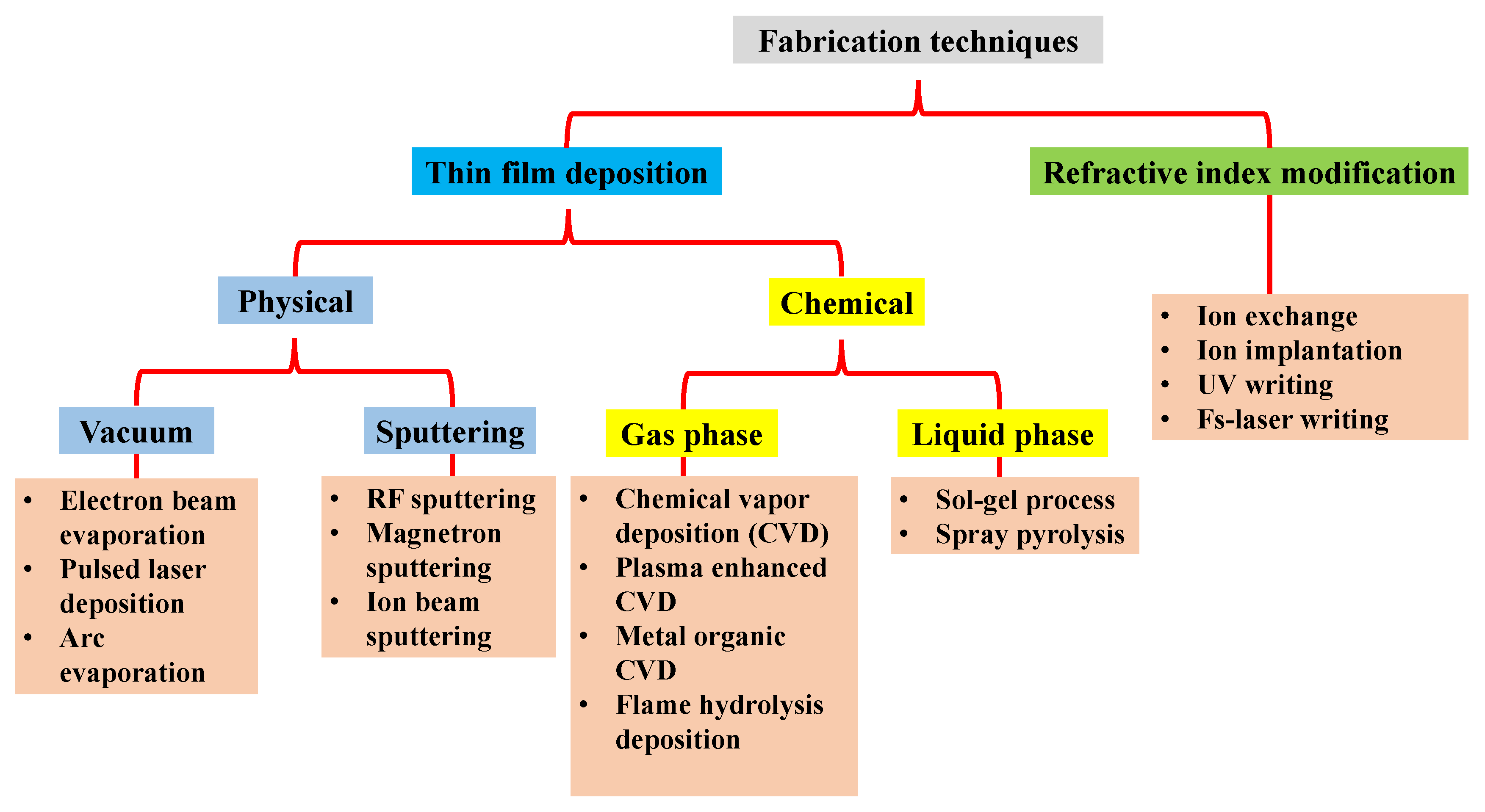
2. Optical Waveguide Layers Fabrication Methods
2.1. Thin-Film Deposition Techniques
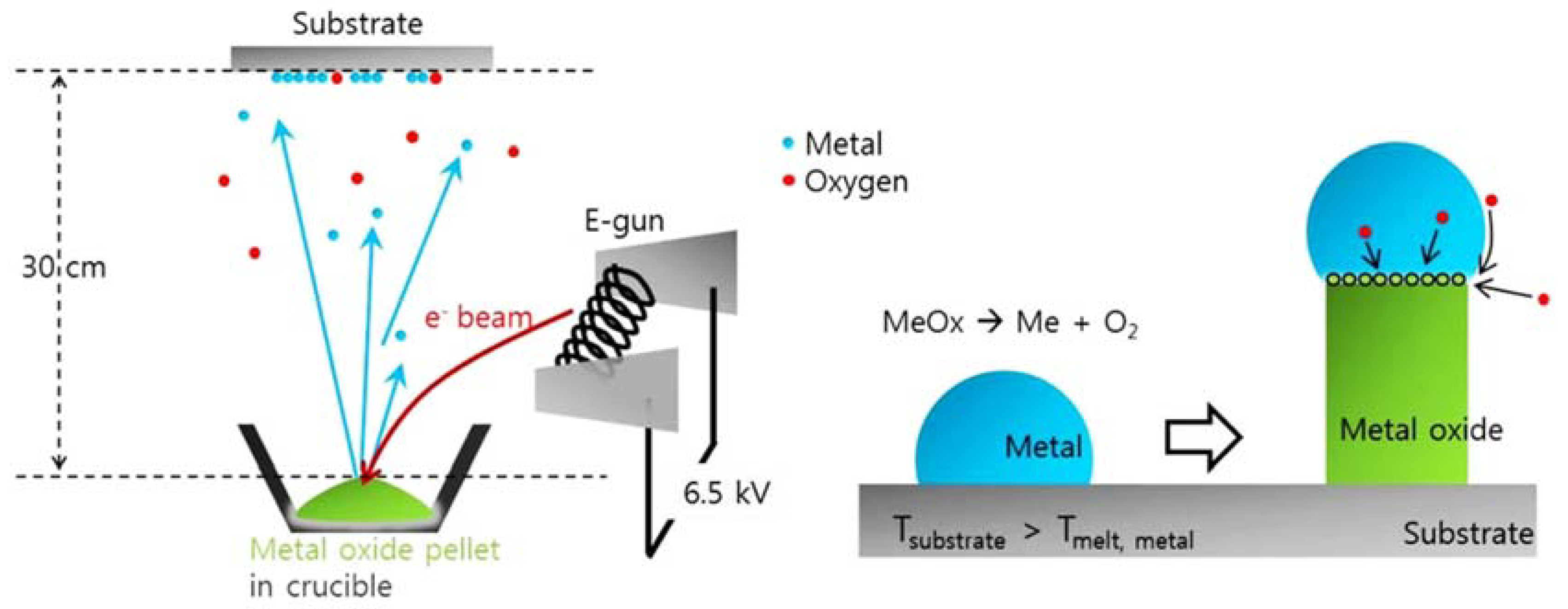
2.1.1. Physical Vapor Deposition Techniques (PVD)
- A.
- Vacuum
- B.
- Sputtering techniques
2.1.2. Chemical Deposition Techniques
- A.
- Gas-phase
- B.
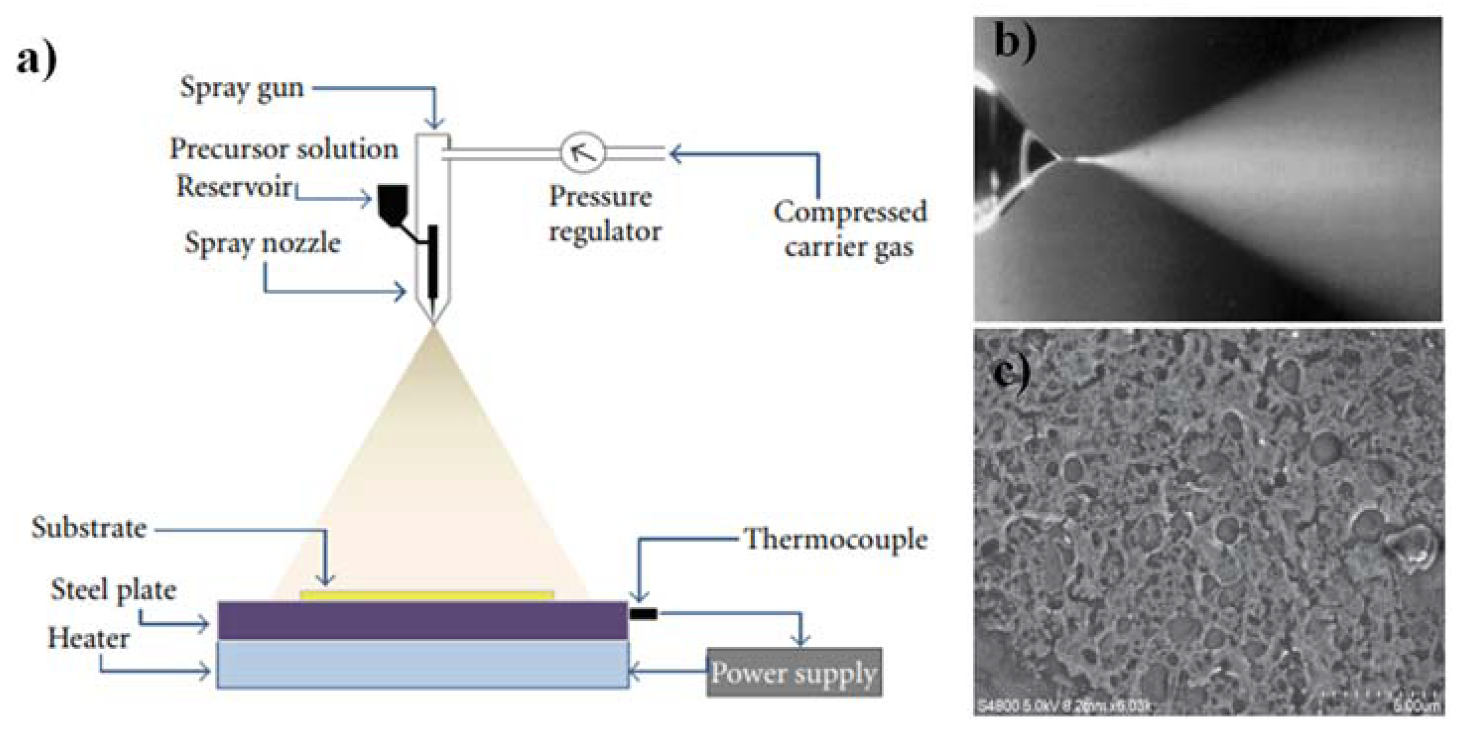
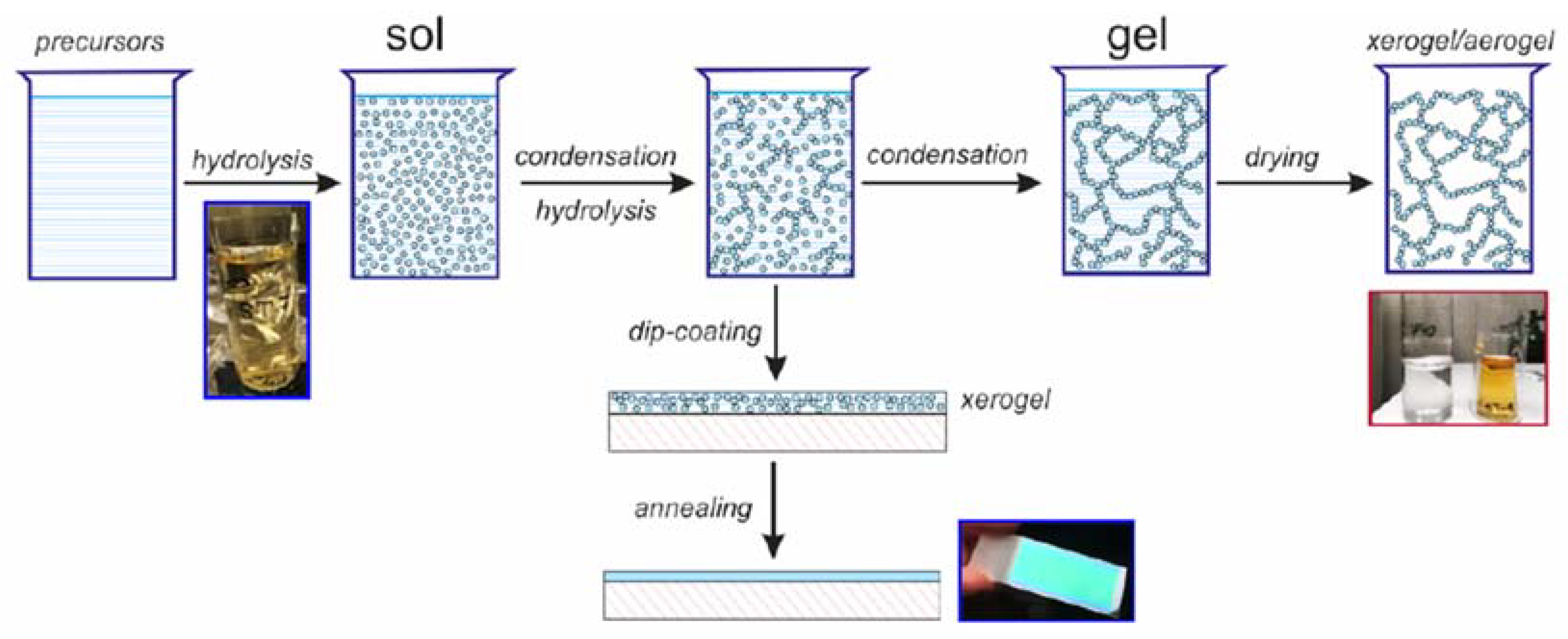
- Liquid-phase deposition
2.2. Refractive Index Modification Methods
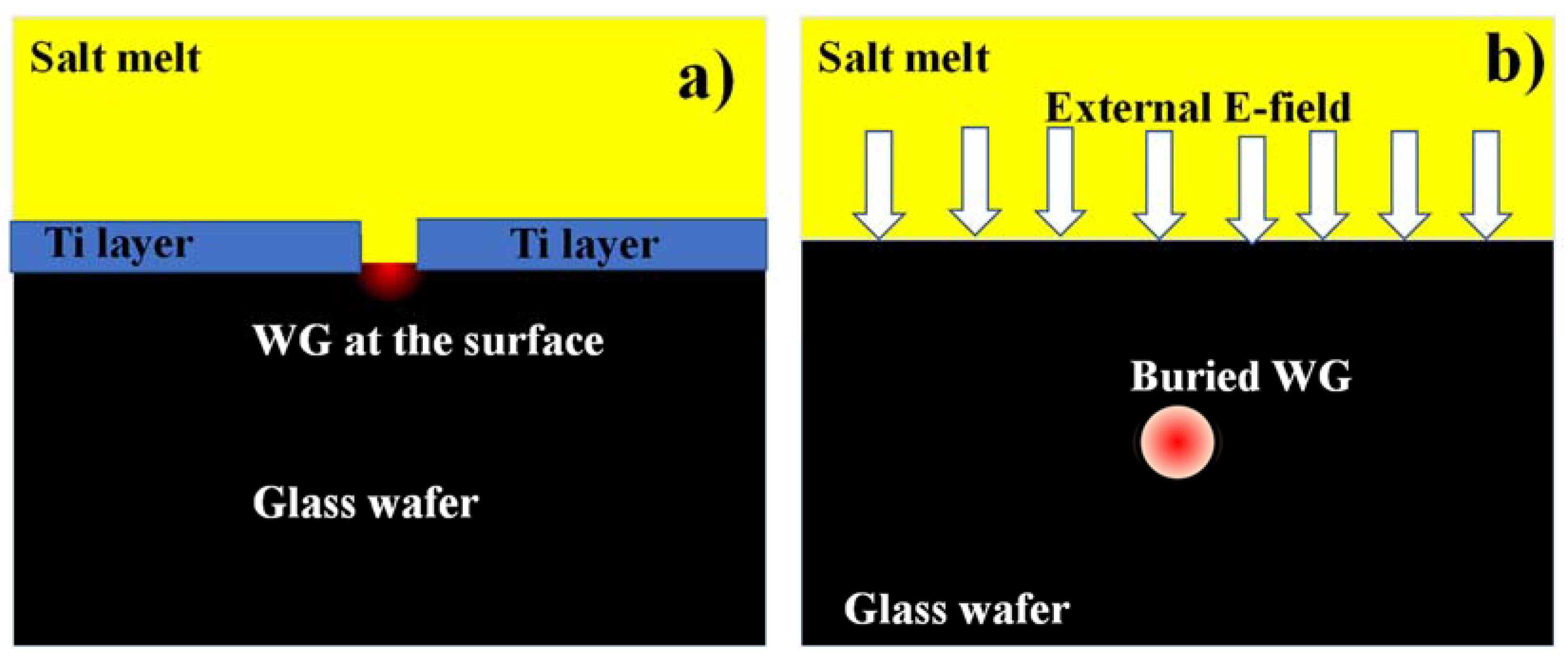
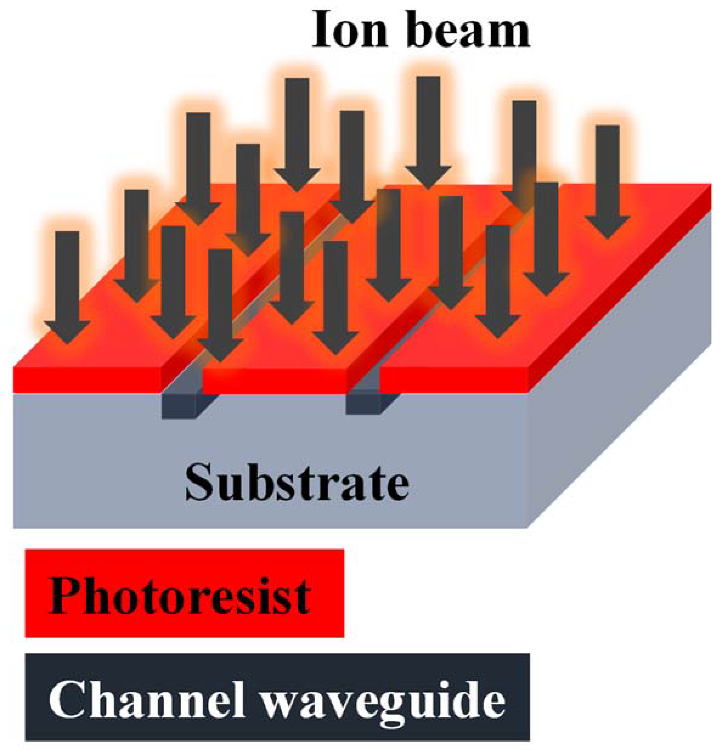
2.2.1. Ion Exchange Process
2.2.2. Ion Implantation
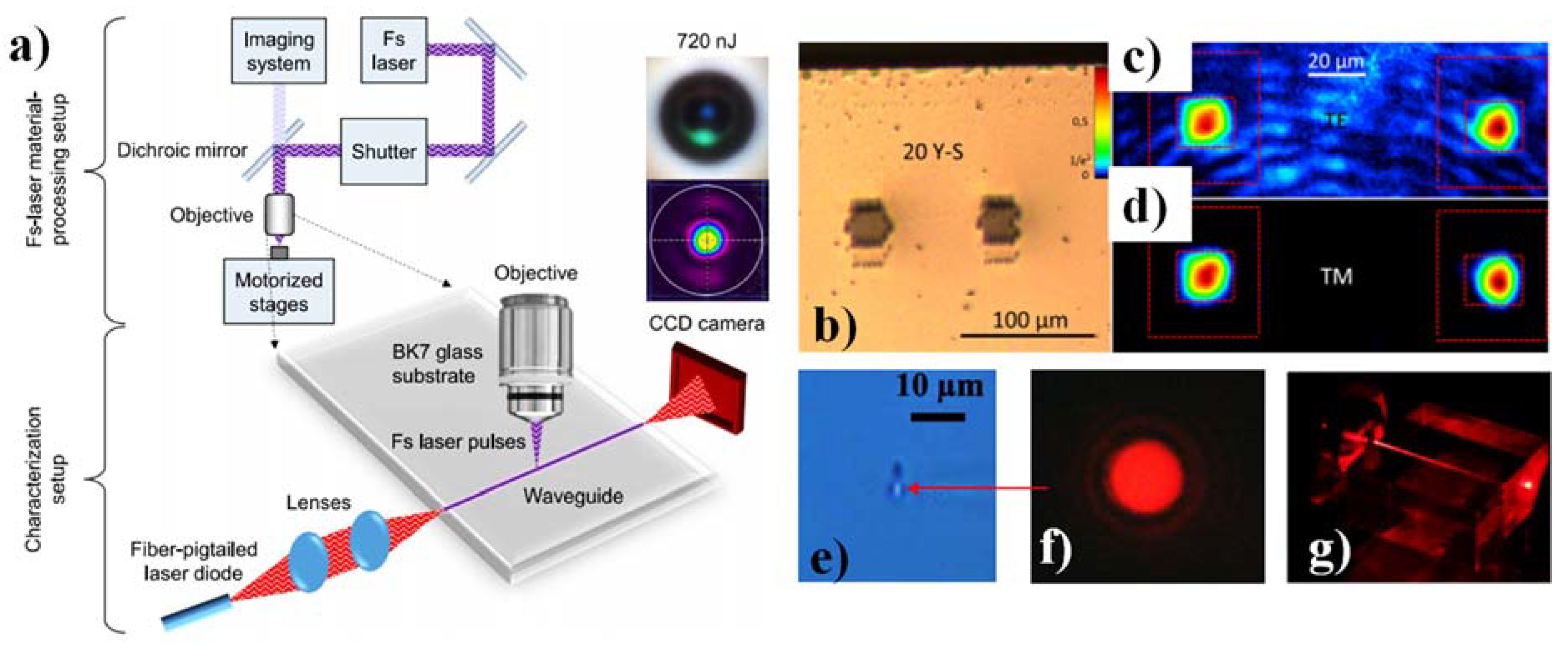
2.2.3. Femtosecond-Laser Writing
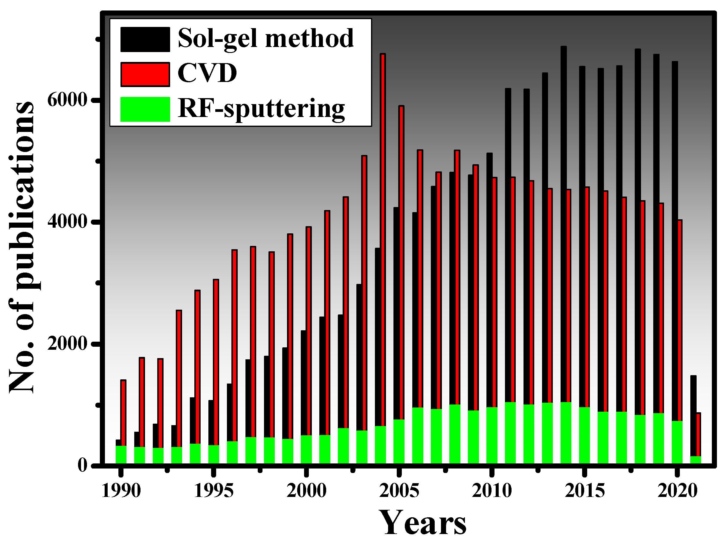
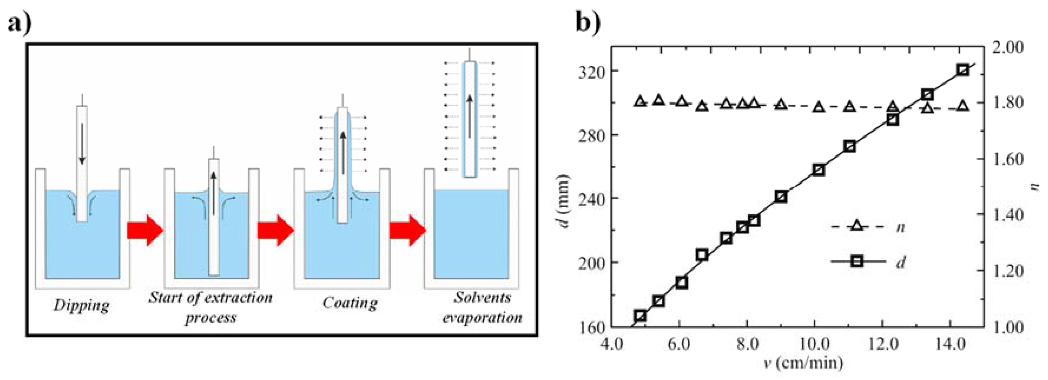
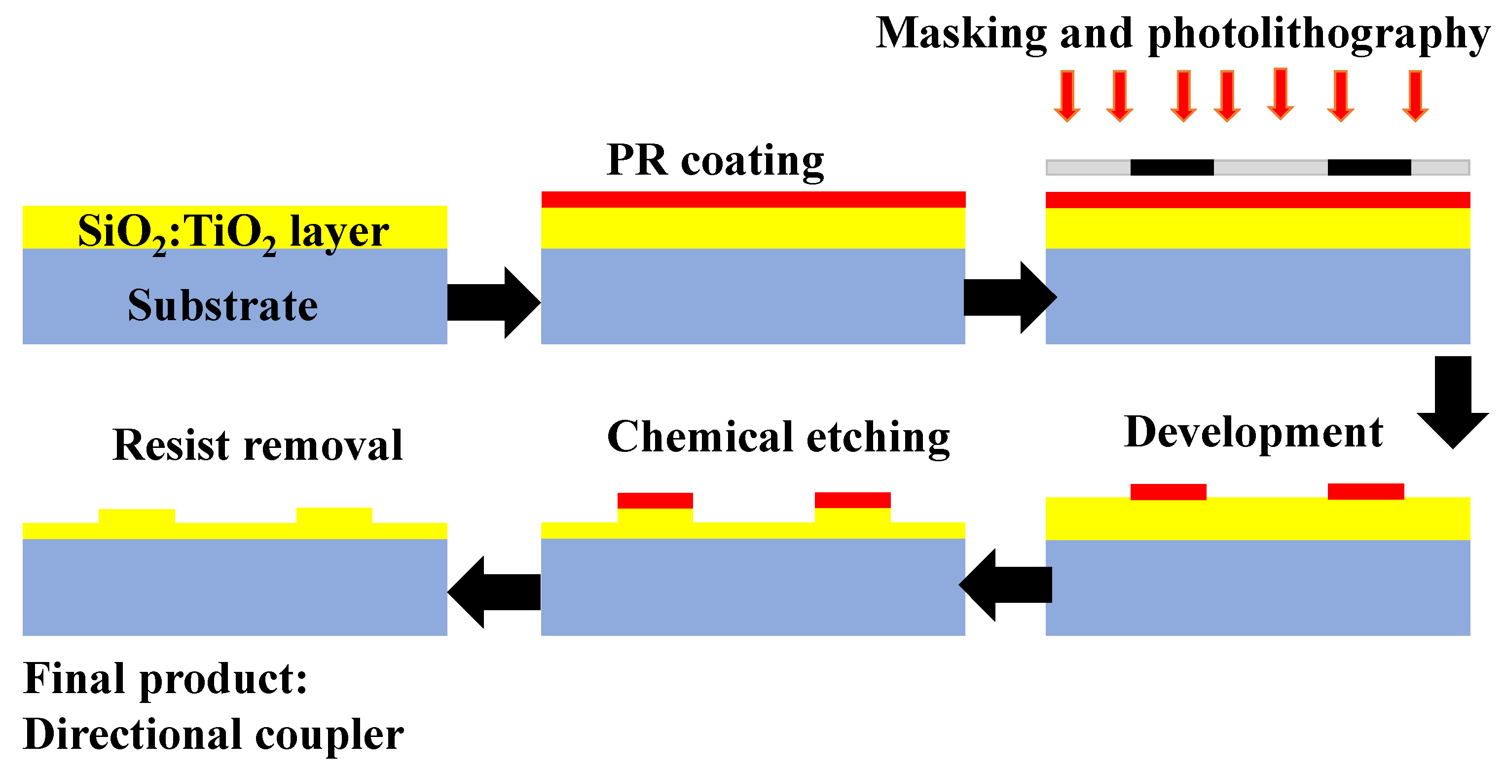
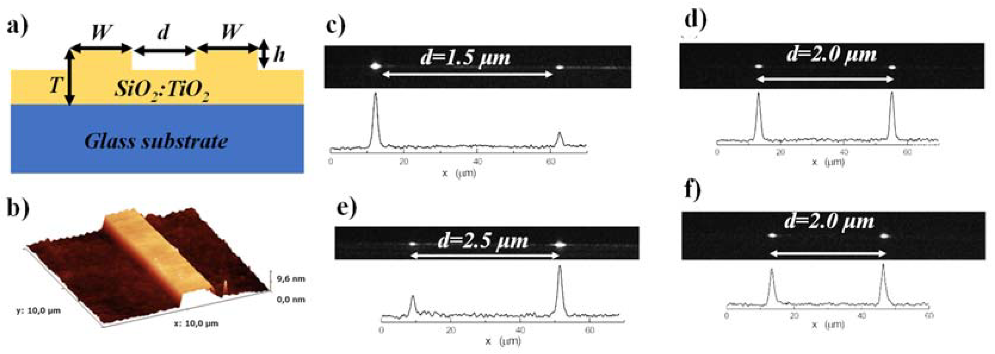
3. Author’s Commentary on Silica-Titania Optical Platform Development via a Sol-gel Dip-Coating Method
4. Future Goals and Challenges
5. Conclusions
Funding
Institutional Review Board Statement
Informed Consent Statement
Data Availability Statement
Acknowledgments
Conflicts of Interest
Abbreviations
References
- Preston, K.; Manipatruni, S.; Gondarenko, A.; Poitras, C.B.; Lipson, M. Deposited silicon high-speed integrated electro-optic modulator. Opt. Express 2009, 17, 5118–5124. [Google Scholar] [CrossRef] [PubMed] [Green Version]
- Hodara, H.; Mitchell, G. Data Centers and beyond, Optical Fiber Communications Breakthroughs from OFC 2019. Fiber Integr. Opt. 2019, 38, 149–190. [Google Scholar] [CrossRef]
- Doerr, C.R. Silicon photonic integration in telecommunications. Front. Phys. 2015, 3, 37. [Google Scholar] [CrossRef]
- Andrews, R.; Milton, A.; Giallorenzi, T. Military Applications of Fiber Optics and Integrated Optics. IEEE Trans. Microw. Theory Tech. 1973, 21, 763–769. [Google Scholar] [CrossRef]
- Finn, G.G. An integration of network communication with workstation architecture. ACM SIGCOMM Comput. Commun. Rev. 1991, 21, 18–29. [Google Scholar] [CrossRef]
- Butt, M.A.; Khonina, S.; Kazanskiy, N. Optical elements based on silicon photonics. Comput. Opt. 2019, 43, 1079–1083. [Google Scholar] [CrossRef]
- Valette, S.; Renard, S.; Jadot, J.; Gidon, P.; Erbeia, C. Silicon-based integrated optics technology for optical sensor applications. Sens. Actuators A Phys. 1990, 23, 1087–1091. [Google Scholar] [CrossRef]
- Butt, M.A.; Khonina, S.N.; Kazanskiy, N.L. Numerical analysis of a miniaturized design of a Fabry–Perot resonator based on silicon strip and slot waveguides for bio-sensing applications. J. Mod. Opt. 2019, 66, 1172–1178. [Google Scholar] [CrossRef]
- Wang, J. Integrated optical signal processing with silicon platform. In Proceedings of the 2016 Progress in Electromagnetic Research Symposium (PIERS), Shanghai, China, 8–11 August 2016; p. 2357. [Google Scholar] [CrossRef]
- El-Derhalli, H.; Beux, S.L.; Tahar, S. Stochastic computing with integrated optics. In Proceedings of the 2019 Design, Automation & Test in Europe Conference & Exhibition (DATE), Florence, Italy, 25–29 March 2019; pp. 1355–1360. [Google Scholar]
- Kazanskiy, N.L.; Butt, M.A. One-dimensional photonic crystal waveguide based on SOI platform for transverse magnetic polarization-maintaining devices. Photon.-Lett. Pol. 2020, 12, 85–87. [Google Scholar] [CrossRef]
- Xu, L.; Wang, Y.; El-Fiky, E.; Mao, D.; Kumar, A.; Xing, Z.; Saber, M.G.; Jacques, M.; Plant, D.V. Compact braodband polarization beam splitter based on multimode interference coupler with internal photonic crystal for the SOI platform. J. Lightw. Technol. 2019, 37, 1231–1240. [Google Scholar] [CrossRef]
- Kazanskiy, N.; Butt, M.; Khonina, S. Silicon photonic devices realized on refractive index engineered subwavelength grating waveguides-A review. Opt. Laser Technol. 2021, 138, 106863. [Google Scholar] [CrossRef]
- Kaźmierczak, A.; Słowikowski, M.; Pavłov, K.; Filipiak, M.; Vervaeke, M.; Tyszkiewicz, C.; Ottevaere, H.; Piramidowicz, R.; Karasiński, P. Efficient, low-cost optical coupling mechanism for TiO2-SiO2 sol-gel derived slab waveguide surface grating coupler sensors. Opt. Appl. 2020, 50, 539–549. [Google Scholar] [CrossRef]
- Kaźmierczak, A.; Słowikowski, M.; Pavłov, K.; Filipiak, M.; Piramidowicz, R. Polymer micro-lenses as an long-coupling-distance interfacing layer in low-cost optical coupling solution between optical fibers and photonic integrated waveguide circuits. Photon.-Lett. Pol. 2019, 11, 121–123. [Google Scholar] [CrossRef]
- Butt, M.A.; Kozlova, E.S.; Khonina, S.N. Conditions of a single-mode rib channel waveguide based on dielectric TiO2/SiO2. Comput. Optics. 2017, 41, 494–498. [Google Scholar] [CrossRef]
- Butt, M.A.; Sole, R.; Pujol, M.C.; Rodenas, A.; Lifante, G.; Choudhary, A.; Murugan, G.S.; Shepherd, D.P.; Wilkinson, J.S.; Aguilo, M.; et al. Fabrication of Y-splitters and Mach-Zehnder structures on (Yb, Nb):RbTiOPO4/RbTiOPO4 epitaxial layers by reactive ion etching. J. Lightwave Technol. 2015, 33, 1863–1871. [Google Scholar] [CrossRef]
- Butt, M.A.; Pujol, M.C.; Solé, R.; Ródenas, A.; Lifante, G.; Wilkinson, J.S.; Aguiló, M.; Díaz, F. Channel waveguides and Mach-Zehnder structures on RbTiOPO_4 by Cs^+ ion exchange. Opt. Mater. Express 2015, 5, 1183. [Google Scholar] [CrossRef]
- Butt, M.A.; Nguyen, H.-D.; Ródenas, A.; Romero, C.; Moreno, P.; De Aldana, J.R.V.; Aguiló, M.; Solé, R.M.; Pujol, M.C.; Díaz, F. Low-repetition rate femtosecond laser writing of optical waveguides in KTP crystals: Analysis of anisotropic refractive index changes. Opt. Express 2015, 23, 15343–15355. [Google Scholar] [CrossRef]
- Han, X.-Y.; Wu, Z.-L.; Yang, S.-C.; Shen, F.-F.; Liang, Y.-X.; Wang, L.-H.; Wang, J.-Y.; Ren, J.; Jia, L.-Y.; Zhang, H.; et al. Recent progress of imprinted polymer photonic waveguide devices and applications. Polymers 2018, 10, 603. [Google Scholar] [CrossRef] [Green Version]
- Righini, G.C.; Chiappini, A. Glass optical waveguides: A review of fabrication techniques. Opt. Eng. 2014, 53, 071819. [Google Scholar] [CrossRef]
- Wang, Y.; Shen, Y.; Zheng, R.-L.; Shen, J.-P.; Guo, H.-T.; Liu, C.-X. Optical characteristics of an oxyfluoride glass waveguide formed by a proton implantation. Results Phys. 2018, 10, 200–204. [Google Scholar] [CrossRef]
- Butt, M.A.; Kazanskiy, N.L. Mode sensitivity analysis of vertically arranged double hybrid plasmonic waveguide. Optoelectron. Adv. Mater. Rapid Commun. 2020, 14, 385–388. [Google Scholar]
- Butt, M.A.; Kazanskiy, N.L.; Khonina, S.N. Highly Sensitive Refractive Index Sensor Based on Plasmonic Bow Tie Configuration. Photon.-Sens. 2020, 10, 223–232. [Google Scholar] [CrossRef]
- Butt, M.A.; Khonina, S.N.; Kazanskiy, N.L. A multichannel metallic dual nano-wall square split-ring resonator: Design analysis and applications. Laser Phys. Lett. 2019, 16, 126201. [Google Scholar] [CrossRef]
- Butt, M.A.; Khonina, S.N.; Kazanskiy, N.L. Highly sensitive refractive index sensor based on hybrid plasmonic waveguide microring resonator. Waves Random Complex. Media 2018, 30, 292–299. [Google Scholar] [CrossRef]
- Butt, M.A.; Kazanskiy, N.L.; Khonina, S.N. Modal Characteristics of Refractive Index Engineered Hybrid Plasmonic Waveguide. IEEE Sens. J. 2020, 20, 9779–9786. [Google Scholar] [CrossRef]
- Butt, M.A.; Fomchenkov, S.A. A polarization-independent highly sensitive hybrid plasmonic waveguide structure. In Proceedings of the 7th International School and Conference “Saint Petersburg OPEN 2020”: Optoelectronics, Photonics, Engineering and Nanostructures, Saint Petersburg, Russia, 27–30 April 2020. [Google Scholar]
- Jilani, A.; Abdel-Wahab, M.S.; Hammad, A.H. Advance deposition techniques for thin film and coating. In Modern Technologies for Creating the Thin Film Systems and Coatings; IntechOpen: London, UK, 2017; pp. 137–149. [Google Scholar]
- Frey, H. Applications and Developments of Thin Film Technology. In Handbook of Thin-Film Technology; Frey, H., Khan, H.R., Eds.; Springer: Berlin/Heidelberg, Germany, 2015; pp. 1–3. [Google Scholar] [CrossRef]
- Veiko, V.P.; Predko, K.G.; Volkov, V.P.; Skiba, P.A. Laser formation of micro-optical elements based on glass-ceramics materials. In Miniature and Micro-Optics: Fabrication and System Applications II; SPIE: Bellingham, WI, USA, 1993; Volume 1751, pp. 361–369. [Google Scholar] [CrossRef]
- Tandon, P.; Boek, H. Experimental and theoretical studies of flame hydrolysis deposition process for making glasses for optical planar devices. J. Non-Cryst. Solids 2003, 317, 275–289. [Google Scholar] [CrossRef]
- Ruano, J.M.; Benoit, V.; Aitchison, J.S.; Cooper, J.M. Flame hydrolysis deposition of glass on silicon for the integration of optical and microfluidic devices. Anal. Chem. 2000, 72, 1093–1097. [Google Scholar] [CrossRef]
- Blocher, J.M., Jr. Coating of glass by chemical vapor deposition. Thin Solid Films 1981, 77, 51–64. [Google Scholar] [CrossRef]
- Karasinski, P.; Tyszkiewicz, C.; Piramidowicz, R.; Kazmierczak, A. Development of integrated photonics based on SiO2-TiO2 sol-gel derived waveguide layers:state of the art, perspectives, prospective applications. In Integrated Photonics Platforms: Fundamental Research, Manufacturing and Applications; SPIE-International Society for Optics and Photonics: Washington, WA, USA, 2020. [Google Scholar]
- Hunsperger, R.G. Waveguide fabrication techniques. In Integrated Optics; Advanced texts in Physics; Springer: Berlin/Heidelberg, Germany, 2002. [Google Scholar]
- Butt, M.A.; Khonina, S.N.; Kazanskiy, N.L. Modelling of rib channel waveguides based on silicon-on-sapphire at 4.67 um wavelength for evanescent field gas absorption sensor. Optik 2018, 168, 692–697. [Google Scholar] [CrossRef]
- Butt, M.A.; Degtyarev, S.A.; Khonina, S.N.; Kazanskiy, N.L. An evanescent field absorption gas sensor at mid-IR 3.39 um wavelength. J. Mod. Opt. 2017, 64, 1892–1897. [Google Scholar] [CrossRef]
- Butt, M.A.; Khonina, S.N.; Kazanskiy, N.L. Silicon on silicon dioxide slot waveguide evanescent field gas absorption sensor. J. Mod. Opt. 2017, 65, 174–178. [Google Scholar] [CrossRef]
- Hao, R.; Zhu, L.; Li, Z.; Fang, F.; Zhang, X. A Miniaturized and fast system for thin film thickness measurement. Appl. Sci. 2020, 10, 7284. [Google Scholar] [CrossRef]
- Boolchandani, S.; Srivastava, S.; Vijay, Y.K. Preparation on InSe thin films by thermal evaporation method and their characterization: Structural, optical, and thermoelectrical properties. J. Nanotechnol. 2018, 2018, 9380573. [Google Scholar] [CrossRef] [Green Version]
- Ali, N.; Teixeira, J.A.; Addali, A.; Saeed, M.; Al-Zubi, F.; Sedaghat, A.; Bahzad, H. Deposition of stainless steel thin films: An electron beam physical vapour deposition approach. Materials 2019, 12, 571. [Google Scholar] [CrossRef] [Green Version]
- Ogugua, S.N.; Ntwaeaborwa, O.M.; Swart, H.C. Latest development on pulsed laser deposited thin films for advanced luminescence applications. Coatings 2020, 10, 1078. [Google Scholar] [CrossRef]
- Opel, M.; Geprägs, S.; Althammer, M.; Brenninger, T.; Gross, R. Laser molecular beam epitaxy of ZnO thin films and heterostructures. J. Phys. D Appl. Phys. 2013, 47, 034002. [Google Scholar] [CrossRef] [Green Version]
- Martin, P.M. Handbook of deposition technologies for films and coatings (Third edition). In Science, Applications and Technology; Elsevier Inc.: Amsterdam, The Netherlands, 2010; pp. 297–313. [Google Scholar]
- Randhawa, H.; Bunshah, R.; Brock, D.; Basol, B.; Stafsudd, O. Preparation of CuxS thin films by activated reactive evaporation technique. Sol. Energy Mater. 1982, 6, 445–453. [Google Scholar] [CrossRef]
- Paul, R.; Hossain, M.; Muktadir, M.; Faisal, K. Fabrication of a cost effective thermal evaporation system for thin film deposition. In Proceedings of the 4th International Conference on Advances in Electrical Engineering (ICAEE), Dhaka, Bangladesh, 28–30 September 2017; pp. 703–706. [Google Scholar]
- Yu, H.K.; Lee, J.-L. Growth mechanism of metal-oxide nanowires synthesized by electron beam evaporation: A self-catalytic vapor-liquid-solid process. Sci. Rep. 2014, 4, 6589. [Google Scholar] [CrossRef] [Green Version]
- Komalakrishna, H.; Augustin, A.; Udaya, B.K. Electron beam deposition of copper thin film on Aluminium substrate and its characterization. Am. J. Mater. Sci. 2015, 5, 19–24. [Google Scholar]
- Sharma, P.; Tripathi, N.; Gupta, N. Nanocrystalline silicon thin film prepared by e-beam evaporation for display application. J. Mater. Sci. Mater. Electron. 2016, 28, 3891–3896. [Google Scholar] [CrossRef]
- Katzer, D.S.; Meyer, D.J.; Storm, D.F.; Nepal, N.; Wheeler, V.D. Silicon nitride thin films deposited using electron-beam evaporation in an RF plasma MBE system. J. Vac. Sci. Technol. B Nanotechnol. Microelectron. Mater. Process. Meas. Phenom. 2014, 32, 02C117. [Google Scholar] [CrossRef]
- Souk, J.H.; O’Hanlon, J.F.; Angillelo, J. Characterization of electron-beam deposited tungsten films on sapphire and silicon. J. Vac. Sci. Technol. A 1985, 3, 2289. [Google Scholar] [CrossRef]
- Sontheimer, T.; Becker, C.; Ruske, F.; Klimm, C.; Bloeck, U.; Gall, S.; Kunz, O.; Young, T.; Egan, R.; Hupkes, J.; et al. Challenges and opportunities of electron beam evaporation in the preparation of poly-Si thin film solar cells. In Proceedings of the 2010 35th IEEE Photovoltaic Specialists Conference, Honolulu, HI, USA,, 20–25 June 2010; pp. 000614–000619. [Google Scholar] [CrossRef]
- Sidqi, N.; Clark, C.; Buller, G.S.; Thalluri, G.K.V.V.; Mitrofanov, J.; Noblet, Y. Comparative study of dielectric coating materials for micro-cavity applications. Opt. Mater. Express 2019, 9, 3452–3468. [Google Scholar] [CrossRef]
- Shamala, K.; Murthy, L.; Rao, K.N. Studies on optical and dielectric properties of Al2O3 thin films prepared by electron beam evaporation and spray pyrolysis method. Mater. Sci. Eng. B 2004, 106, 269–274. [Google Scholar] [CrossRef] [Green Version]
- Ashfold, M.N.R.; Claeyssens, F.; Fuge, G.M.; Henley, S.J. Pulsed laser ablation and deposition of thin films. Chem. Soc. Rev. 2003, 33, 23–31. [Google Scholar] [CrossRef] [Green Version]
- Rao, M.C. Pulsed laser deposition—Ablation mechanism and applications. Int. J. Mod. Phys. Conf. Ser. 2013, 22, 355–360. [Google Scholar] [CrossRef]
- Snigirev, O.; Chukharkin, M.; Porokhov, N.; Rusanov, S.Y.; Kashin, V.V.; Tsvetkov, V.B.; Kalabukhov, A.; Winkler, D. Pulsed laser deposition of thin YBCO films on faceted YSZ single crystal fibers. In Journal of Physics: Conference Series; IOP Publishing: Bristol, UK, 2014; Volume 507. [Google Scholar] [CrossRef] [Green Version]
- Fulton, M.L. New ion-assisted filtered cathodic arc deposition (IFCAD) technology for producing advanced thin films on temperature-sensitive substrates. In Solar Optical Materials XVI; SPIE: Bellingham, WA, USA, 1999; Volume 3789, pp. 29–38. [Google Scholar] [CrossRef]
- Fulton, M.L. Review of cathodic arc deposition. In Optical Interference Coatings; OSA Technical Digest Series; Springer: Banff, AB, Canada, 2001. [Google Scholar]
- Xia, A.; Glushko, O.; Cordill, M.J.; Franz, R. Electromechanical properties of cathodic arc deposited high entropy alloy thin films on polymer substrates. J. Vac. Sci. Technol. A Vac. Surf. Films 2019, 37, 010601. [Google Scholar] [CrossRef] [Green Version]
- Huang, C.-W.; Yang, R.-Y.; Pan, C.-T.; Weng, M.-H. Effect of O2/Ar gas flow ratios on properties of cathodicvacuum arc deposited ZnO thin films on polyethylene terephthalate substrate. J. Nanomater. 2016, 2016, 6479812. [Google Scholar] [CrossRef] [Green Version]
- Vattanaprateep, N.; Panich, N.; Surinphong, S.; Tungasmita, S.; Wangyao, P. Structural and mechanical properties of nanostructured TiAlCrN thin films deposited by cathodic arc deposition. High. Temp. Mater. Process. 2013, 32, 107–111. [Google Scholar] [CrossRef]
- Rosén, J.; Mráz, S.; Kreissig, U.; Music, D.; Schneider, J. Effect of ion energy on structure and composition of cathodic arc deposited alumina thin films. Plasma Chem. Plasma Process. 2005, 25, 303–317. [Google Scholar] [CrossRef]
- Brzezinka, T.L.; Rao, J.; Paiva, J.M.; Azkona, I.; Kohlscheen, J.; Rabinovich, G.S.F.; Veldhuis, S.C.; Endrino, J.L. Facilitating TiB2 for filtered vacuum cathodic arc evaporation. Coatings 2020, 10, 244. [Google Scholar] [CrossRef] [Green Version]
- Takikawa, H.; Tanoue, H. Review of cathodic arc deposition for preparing droplet-free thin films. IEEE Trans. Plasma Sci. 2007, 35, 992–999. [Google Scholar] [CrossRef]
- Gulkowski, S.; Krawczak, E. RF/DC magnetron sputtering deposition of thin layers for solar cell fabrication. Coatings 2020, 10, 791. [Google Scholar] [CrossRef]
- Zagho, M.M.; Dawoud, H.D.; Bensalah, N.; Altahtamouni, T.M. A brief overview of RF sputtering deposition of boron carbon nitride (BCN) thin films. Emergent Mater. 2018, 2, 79–93. [Google Scholar] [CrossRef] [Green Version]
- Khan, N.A.; Akhavan, B.; Zhou, C.; Zhou, H.; Chang, L.; Wang, Y.; Liu, Y.; Fu, L.; Bilek, M.M.; Liu, Z. RF magnetron sputtered AlCoCrCu0.5FeNi high entropy alloy (HEA) thin films with tuned microstructure and chemical composition. J. Alloy. Compd. 2020, 836, 155348. [Google Scholar] [CrossRef]
- Srivastava, P.K.; Vankar, V.D.; Chopra, K.L. R.F. magnetron sputtered tungsten carbide thin films. Bull. Mater. Sci. 1986, 8, 379–384. [Google Scholar] [CrossRef]
- Kylián, O.; Shelemin, A.; Solař, P.; Pleskunov, P.; Nikitin, D.; Kuzminova, A.; Štefaníková, R.; Kúš, P.; Cieslar, M.; Hanuš, J.; et al. Magnetron sputtering of polymeric targets: From thin films to heterogeneous metal/plasma polymer nanoparticles. Materials 2019, 12, 2366. [Google Scholar] [CrossRef] [Green Version]
- Subbarayudu, S.; Madhavi, V.; Uthanna, S. Growth of MoO3 films by RF magnetron sputtering: Studies on the structural, optical, and electrochromic properties. Int. Sch. Res. Not. 2013, 2013, 806374. [Google Scholar] [CrossRef] [Green Version]
- Abdullah, S.; Nafarizal, N.; Sahdan, M.Z. Influence of Oxygen flow rate on the characteristics of the tungsten oxide using RF magnetron sputtering. Appl. Mech. Mater. 2015, 773–774, 657–661. [Google Scholar] [CrossRef] [Green Version]
- Sproul, W.; Christie, D.; Carter, D. Control of reactive sputtering processes. Thin Solid Films 2005, 491, 1–17. [Google Scholar] [CrossRef]
- Chen, S.; Tao, L.; Zeng, L.; Hong, R. RF magnetron sputtering aluminum oxide film for surface passivation on crystalline silicon wafers. Int. J. Photoenergy 2013, 2013, 792357. [Google Scholar] [CrossRef]
- Mobtakeri, S.; Akaltun, Y.; Özer, A.; Kılıç, M.; Tüzemen, E.; Gür, E. Gallium oxide films deposition by RF magnetron sputtering; a detailed analysis on the effects of deposition pressure and sputtering power and annealing. Ceram. Int. 2020, 47, 1721–1727. [Google Scholar] [CrossRef]
- Nur-E-Alam, M.; Lonsdale, W.; Vasiliev, M.; Alameh, K. Application-Specific oxide-based and metal–dielectric thin-film materials prepared by radio frequency magnetron sputtering. Materials 2019, 12, 3448. [Google Scholar] [CrossRef] [PubMed] [Green Version]
- Greene, J.E. Review Article: Tracing the recorded history of thin-film sputter deposition: From the 1800s to 2017. J. Vac. Sci. Technol. A Vac. Surf. Films 2017, 35, 05C204. [Google Scholar] [CrossRef] [Green Version]
- Cevro, M.; Carter, G. Ion beam sputtering and dual ion beam sputtering of titanium oxide films. J. Phys. D Appl. Phys. 1995, 28, 1962–1976. [Google Scholar] [CrossRef]
- Ensinger, W. Ion sources for ion beam assisted deposition of thin films and coatings (invited) (abstract). Rev. Sci. Instrum. 1992, 63, 2380. [Google Scholar] [CrossRef]
- Hirvonen, J.K. Ion beam Assisted Thin film deposition. In Materials and Processes for Surface and Interface Engineering; NATO ASI Series (Series E: Applied Sciences); Pauleau, Y., Ed.; Springer: Dordrecht, The Netherlands, 1991; pp. 215–274. [Google Scholar]
- Ali, M.Y.; Hung, W.; Yongqi, F. A review of focused ion beam sputtering. Int. J. Precis. Eng. Manuf. 2010, 11, 157–170. [Google Scholar] [CrossRef]
- Lin, L.; Deng, B.; Sun, J.; Peng, H.; Liu, Z. Bridging the gap between reality and ideal in chemical vapor deposition growth of graphene. Chem. Rev. 2018, 118, 9281–9343. [Google Scholar] [CrossRef]
- Woehrl, N.; Ochedowski, O.; Gottlieb, S.; Shibasaki, K.; Schulz, S. Plasma-enhanced chemical vapor deposition of graphene on copper substrates. AIP Adv. 2014, 4, 047128. [Google Scholar] [CrossRef] [Green Version]
- Cohen, A.; Patsha, A.; Mohapatra, P.K.; Kazes, M.; Ranganathan, K.; Houben, L.; Oron, D.; Ismach, A. Growth-etch metal-organic chemical vapor deposition approach of WS2 atomic layers. ACS Nano 2021, 15, 526–538. [Google Scholar] [CrossRef]
- Okada, H.; Baba, M.; Furukawa, M.; Yamane, K.; Sekiguchi, H.; Wakahara, A. Formation of SiO2 film by chemical vapor deposition enhanced by atomic species extracted from a surface-wave generated plasma. AIP Conf. Proc. 2017, 1807, 020006. [Google Scholar] [CrossRef] [Green Version]
- Matsuura, Y.; Harrington, J.A. Hollow glass waveguides with three-layer dielectric coating fabricated by chemical vapor deposition. J. Opt. Soc. Am. A 1997, 14, 1255–1259. [Google Scholar] [CrossRef]
- Matsuura, Y.; Harrington, J.A. Infrared hollow glass waveguides fabricated by chemical vapor deposition. Opt. Lett. 1995, 20, 2078–2080. [Google Scholar] [CrossRef] [PubMed]
- Gismatulin, A.A.; Kamaev, G.N.; Kruchinin, V.N.; Gritsenko, V.A.; Orlov, O.M.; Chin, A. Charge transport mechanism in the forming-free memristor based on silicon nitride. Sci. Rep. 2021, 11, 2417. [Google Scholar] [CrossRef]
- Bigiani, L.; Barreca, D.; Gasparotto, A.; Andreu, T.; Verbeeck, J.; Sada, C.; Modin, E.; Lebedev, O.I.; Morante, J.R.; Maccato, C. Selective anodes for seawater splitting via functionalization of manganese oxides by a plasma-assisted process. Appl. Catal. B Environ. 2020, 284, 119684. [Google Scholar] [CrossRef]
- Blout, A.; Pulpytel, J.; Mori, S.; Arefi-Khonsari, F.; Méthivier, C.; Pailleret, A.; Jolivalt, C. Carbon nanowalls functionalization for efficient O2 reduction catalyzed by laccase using design of experiment. Appl. Surf. Sci. 2021, 547, 149112. [Google Scholar] [CrossRef]
- Lusk, D.; Gore, M.; Boardman, W.; Casserly, T.; Boinapally, K.; Oppus, M.; Upadhyaya, D.; Tudhope, A.; Gupta, M.; Cao, Y.; et al. Thick DLC films deposited by PECVD on the internal surface of cylindrical substrates. Diam. Relat. Mater. 2008, 17, 1613–1621. [Google Scholar] [CrossRef] [Green Version]
- Selvamanickam, V.; Xie, Y.; Reeves, J.; Chen, Y. MOCVD-Based YBCO-Coated Conductors. MRS Bull. 2004, 29, 579–582. [Google Scholar] [CrossRef]
- Kilian, A.; Kirchof, J.; Przyrembel, G.; Wischmann, W. Birefringence free planar optical waveguide made by flame hydrolysis deposition (FHD) through tailoring of the overcladding. J. Light. Technol. 2000, 18, 193–198. [Google Scholar] [CrossRef]
- Holmes, C.; Gates, J.C.; Smith, P.R. Planarised optical fiber composite using flame hydrolysis deposition demonstrating an integrated FBG anemometer. Opt. Express 2014, 22, 32150–32157. [Google Scholar] [CrossRef] [Green Version]
- Zhang, L.; Xie, W.; Wu, Y.; Xing, H.; Li, A.; Zheng, W. Optical and surface properties of SiO2 by flame hydrolysis deposition for silica waveguide. Opt. Mater. 2003, 22, 283–287. [Google Scholar] [CrossRef]
- Saha, J.K.; Bukke, R.N.; Mude, N.N.; Jang, J. Significant improvement of spray pyrolyzed ZnO thin film by precursor optimization for high mobility thin film transistors. Sci. Rep. 2020, 10, 8999. [Google Scholar] [CrossRef] [PubMed]
- Perednis, D.; Gauckler, L.J. Thin Film Deposition Using Spray Pyrolysis. J. Electroceramics 2005, 14, 103–111. [Google Scholar] [CrossRef]
- Patil, G.E.; Kajale, D.D.; Gaikwad, V.B.; Jain, G.H. Spray Pyrolysis Deposition of Nanostructured Tin Oxide Thin Films. ISRN Nanotechnol. 2012, 2012, 275872. [Google Scholar] [CrossRef] [Green Version]
- Cho, J.; Hwang, S.; Ko, D.-H.; Chung, S. Transparent ZnO Thin-Film Deposition by Spray Pyrolysis for High-Performance Metal-Oxide Field-Effect Transistors. Materials 2019, 12, 3423. [Google Scholar] [CrossRef] [Green Version]
- Filipovic, L.; Selberherr, S.; Mutinati, G.C.; Brunet, E.; Steinhauer, S.; Köck, A.; Teva, J.; Kraft, J.; Siegert, J.; Schrank, F. Methods of simulating thin film deposition using spray pyrolysis techniques. Microelectron. Eng. 2014, 117, 57–66. [Google Scholar] [CrossRef]
- Ramadhani, M.F.; Pasaribu, M.A.H.; Yuliarto, B. Nugraha Fabrication of ZnO nanorod using spray-pyrolysis and chemical bath deposition method. AIP Conference Proceedings 2014, 1586, 74–77. [Google Scholar] [CrossRef]
- Gurav, A.; Kodas, T.; Pluym, T.; Xiong, Y. Aerosol Processing of Materials. Aerosol Sci. Technol. 1993, 19, 411–452. [Google Scholar] [CrossRef]
- Leong, K. Morphological control of particles generated from the evaporation of solution droplets: Theoretical considerations. J. Aerosol Sci. 1987, 18, 511–524. [Google Scholar] [CrossRef]
- Ju, S.H.; Hong, S.K.; Jang, H.C.; Kang, Y.C. Fine size cobalt oxide powders prepared by spray pyrolysis using two types of spray generators. J. Ceram. Soc. Jpn. 2007, 115, 507–510. [Google Scholar] [CrossRef] [Green Version]
- Lengyel, M.; Atlas, G.; Elhassid, D.; Luo, P.; Zhang, X.; Belharouak, I.; Axelbaum, R. Effects of synthesis conditions on the physical and electrochemical properties of Li1.2Mn0.54Ni0.13Co0.13O2 prepared by spray pyrolysis. J. Power Sources 2014, 262, 286–296. [Google Scholar] [CrossRef]
- Zhang, S.-C.; Messing, G.L.; Borden, M. Synthesis of solid, spherical zirconia particles by spray pyrolysis. J. Am. Ceram. Soc. 1990, 73, 61–67. [Google Scholar] [CrossRef]
- Cho, S.-Y.; Kim, I.-T.; Kim, D.-Y.; Park, S.J.; Kim, B.-K.; Lee, J.-H. Effects of H2O2 on the morphology of ZrO2 powder prepared by ultrasonic spray pyrolysis. Mater. Lett. 1997, 32, 271–273. [Google Scholar] [CrossRef]
- Kang, Y.; Roh, H.; Park, S. Preparation of Y2O3:Eu phosphor particles of filled morphology at high precursor concentrations by spray pyrolysis. Adv. Mater. 2000, 12, 451–453. [Google Scholar] [CrossRef]
- Pantano, C.; Ganan-Calvo, A.; Barrero, A. Zeroth-order, electrohydrostatic solution for electrospraying in cone-jet mode. J. Aerosol. Sci. 1994, 25, 1065–1077. [Google Scholar] [CrossRef]
- Ebelmen, M. Sur les combinaisons des acides borique et silicique avec les ethers. Annl. Chim. Phys. 1846, 16, 129–166. [Google Scholar]
- Thor, T.; Vaclavik, J. Sol-gel preparation of silica and titania thin films. In Proceedings of the Optics and Measurement International Conference, Liberec, Czech Republic, 11 November 2016; Volume 10151. [Google Scholar]
- Schroeder, H. Oxide layers deposited from organic solutions. In Physics of thin films: Advances in Research and Developments; Academic Press: London, UK; New York, NY, USA, 1969; pp. 87–141. [Google Scholar]
- Attia, S.M.; Wang, J.; Wu, G.; Shen, J.; Jianhua, M.A. Review on sol-gel derived coatings: Process, techniques and optical applications. J. Mater. Sci. Technol. 2002, 18, 211–217. [Google Scholar]
- Logan, M.N.; Prabakar, S.; Brinker, C.J. Sol-Gel-Derived silica films with tailored microstructures for applications requiring organic dyes. MRS Proc. 1994, 346, 74–77. [Google Scholar] [CrossRef] [Green Version]
- Brinker, C.; Frye, G.; Hurd, A.; Ashley, C. Fundamentals of sol-gel dip coating. Thin Solid Films 1991, 201, 97–108. [Google Scholar] [CrossRef]
- Fidalgo, A.; Ilharco, L.M. The defect structure of sol–gel-derived silica/polytetrahydrofuran hybrid films by FTIR. J. Non-Cryst. Solids 2001, 283, 144–154. [Google Scholar] [CrossRef]
- Parin, R.; Rigon, M.; Bortolin, S.; Martucci, A.; Del Col, D. Optimization of hybrid sol-gel coating for dropwise condensation of pure steam. Materials 2020, 13, 878. [Google Scholar] [CrossRef] [PubMed] [Green Version]
- Acosta, S.; Ayral, A.; Guizard, C.; Lecornec, C.; Passemard, G.; Moussavi, M. Sol-Gel derived silica layers for low-k dielectrics applications. MRS Proc. 2000, 612, D5.26.1–D5.26.6. [Google Scholar] [CrossRef]
- Boudot, M.; Gaud, V.; Louarn, M.; Selmane, M.; Grosso, D. Sol–Gel based hydrophobic antireflective coatings on organic substrates: A detailed investigation of ammonia vapor treatment (AVT). Chem. Mater. 2014, 26, 1822–1833. [Google Scholar] [CrossRef]
- Kim, T.; Song, K. Low-temperature preparation of superhydrophilic coatings using tetraethoxysilane and colloidal silica by sol-gel method. Colloids Surf. A Physicochem. Eng. Asp. 2022, 647, 129105. [Google Scholar] [CrossRef]
- Hasaneen, M.; Shalaby, M.; Yousif, N.; Diab, A.; El Agammy, E. Structural and optical properties of transparent conducting oxide Cd1-xCrxO thin films prepared by the sol-gel dip-coating method. Mater. Sci. Eng. B 2022, 280, 115703. [Google Scholar] [CrossRef]
- Niazmand, M.; Maghsoudipour, A.; Alizadeh, M.; Khahpour, Z.; Kariminejad, A. Effect of dip coating parameters on microstructure and thickness of 8YSZ electrolyte coated on NiO-YSZ by sol-gel process for SOFCs applications. Ceram. Int. 2022, 48, 16091–16098. [Google Scholar] [CrossRef]
- Esfahani, M.B.; Eshaghi, A.; Bakhshi, S.R. Transparent hydrophobic, self-cleaning, anti-icing and anti-dust nano-structured silica based thin film on cover glass solar cell. J. Non-Cryst. Solids 2022, 583, 121479. [Google Scholar] [CrossRef]
- Beldjebli, O.; Bensaha, R.; Panneerselvam, P. Effect of both sn doping and annealing temperature on the properties of dip-coated nanostructured TiO2 thin films. J. Inorg. Organomet. Polym. Mater. 2022, 32, 1624–1636. [Google Scholar] [CrossRef]
- Both, J.; Szabo, G.; Katona, G.; Muresan, L. Tannic acid reinforced sol-gel silica coatings for corrosion protecion of zinc substrates. Mater. Chem. Phys. 2022, 282, 125912. [Google Scholar] [CrossRef]
- Rogozinski, R.; Karasinski, P. Optical waveguides produced in ion exchange process from the solutions of AgNO3-NaNO3 for planar chemical amplitude sensors. Opto-Electron. Rev. 2005, 13, 229–238. [Google Scholar]
- Izawa, T.; Nakagome, H. Optical waveguide formed by eletrically induced migration of ions in glass plates. Appl. Phys. Lett. 1972, 21, 584–586. [Google Scholar] [CrossRef]
- Giallorenzi, T.; West, E.; Kirk, R.; Ginther, R.; Andrews, R. Optical waveguides formed by thermal migration of ions in glass. Appl. Opt. 1973, 12, 1240–1245. [Google Scholar] [CrossRef] [PubMed]
- Findakly, T. Glass Waveguides by Ion Exchange: A Review. Opt. Eng. 1985, 24, 242244. [Google Scholar] [CrossRef]
- Cugat, J.; Solé, R.; Carvajal, J.J.; Mateos, X.; Massons, J.; Lifante, G.; Díaz, F.; Aguiló, M. Channel waveguides on RbTiOPO4 by Cs+ ion exchange. Opt. Lett. 2013, 38, 323–325. [Google Scholar] [CrossRef]
- Du, B.; Tong, Z.; Mu, X.; Xu, J.; Liu, S.; Liu, Z.; Cao, W.; Qi, Z.-M. A potassium ion-exchanged glass optical waveguide sensor locally coated with a crystal violet-SiO2 gel film for real-time detection of organophosphorus pesticides simulant. Sensors 2019, 19, 4219. [Google Scholar] [CrossRef] [Green Version]
- Tervonen, A.; West, B.R.; Honkanen, S. Ion-Exchanged glass waveguide technology: A review. Phys. Comput. Sci. Fac. Publ. Opt. Eng. 2011, 50, 071107. [Google Scholar] [CrossRef] [Green Version]
- Ramaswamy, R.; Srivastava, R. Ion-exchanged glass waveguides: A review. J. Light. Technol. 1988, 6, 984–1000. [Google Scholar] [CrossRef]
- Rehouma, F.; Bentouila, O. Special glass for silver-sodium ion exchanged waveguides. J. King Saud Univ.-Sci. 2018, 32, 433–435. [Google Scholar] [CrossRef]
- Amiri, I.S.; Ariannejad, M.; Ali, J.; Yupapin, P. Design of optical splitter using ion-exchange method for DNA bio-sensor. J. King Saud Univ.-Sci. 2019, 31, 549–555. [Google Scholar] [CrossRef]
- Yulianto, M.; Marzuki, A.; Suryanti, V. Fabrication and characterization planar waveguides of Na+-Ag+/K+ by ion exchange and prism coupler. AIP Conf. Proc. 2017, 1868, 060006. [Google Scholar]
- Jackel, J.L.; Vogel, E.M.; Aitchison, J.S. Ion-exchanged optical waveguides for all-optical switching. Appl. Opt. 1990, 29, 3126–3129. [Google Scholar] [CrossRef] [PubMed]
- Albert, J.; Lit, J.W.Y. Full modeling of field-assisted ion exchange for graded index buried channel optical waveguides. Appl. Opt. 1990, 29, 2798–2804. [Google Scholar] [CrossRef] [Green Version]
- Monteiro, H.S.; Said, J.C.; Mendes, J.F.; Srivastava, R. An apparatus for fabrication of optical waveguides by electromigration. Rev. Sci. Instrum. 1997, 68, 4014–4016. [Google Scholar] [CrossRef]
- Namba, S.; Aritome, H.; Nishimura, T.; Masuda, K.; Toyoda, K. Optical waveguides fabricated by ion implantation. J. Vac. Sci. Technol. 1973, 10, 936–940. [Google Scholar] [CrossRef]
- Bi, Z.-F.; Wang, L.; Liu, X.-H.; Zhang, S.-M.; Dong, M.-M.; Zhao, Q.-Z.; Wu, X.-L.; Wang, K.-M. Optical waveguides in TiO2 formed by He ion implantation. Opt. Express 2012, 20, 6712–6719. [Google Scholar] [CrossRef] [PubMed]
- Chandler, P.J.; Zhang, L.; Townsend, P.D. Double waveguide in LiNbO3 by ion implantation. Appl. Phys. Lett. 1989, 55, 1710–1712. [Google Scholar] [CrossRef]
- Townsend, P.D.; Chandler, P.J.; Zhang, L. Optical Effects of Ion Implantation; Cambridge University Press: Cambridge, UK, 1994. [Google Scholar] [CrossRef]
- Chen, X.; Milosevic, M.M.; Khokhar, A.Z.; Thomson, D.J.; Reed, G.T. Optical Waveguides by Germanium Ion Implantation on Silicon-on-Insulator Platform. In Proceedings of the Conference on Lasers and Electro-Optics/Pacific Rim 2018, Hong Kong, China, 29 July–3 August 2018. [Google Scholar] [CrossRef]
- Jiao, Y.; Wang, L. Optical Channel Waveguide in KTiOAsO4 Crystals Produced by O+ ion Implantation. J. Light. Technol. 2011, 30, 1433–1436. [Google Scholar] [CrossRef]
- Davis, K.M.; Miura, K.; Sugimoto, N.; Hirao, K. Writing waveguides in glass with a femtosecond laser. Opt. Lett. 1996, 21, 1729–1731. [Google Scholar] [CrossRef]
- Gross, S.; Dubov, M.; Withford, M.J. On the use of the Type I and II scheme for classifying ultrafast laser direct-write photonics. Opt. Express 2015, 23, 7767–7770. [Google Scholar] [CrossRef]
- Chen, G.Y.; Piantedosi, F.; Otten, D.; Kang, Y.Q.; Zhang, W.Q.; Zhou, X.; Monro, T.M.; Lancaster, D.G. Femtosecond-laser-written Microstructured Waveguides in BK7 Glass. Sci. Rep. 2018, 8, 10377. [Google Scholar] [CrossRef]
- Ehrt, D.; Kittel, T.; Will, M.; Nolte, S.; Tünnermann, A. Femtosecond-laser-writing in various glasses. J. Non-Cryst. Solids 2004, 345–346, 332–337. [Google Scholar] [CrossRef]
- Fedotov, S.S.; Butvina, L.N.; Okhrimchuk, A.G. Plastic deformation as nature of femtosecond laser writing in YAG crystal. Sci. Rep. 2020, 10, 19385. [Google Scholar] [CrossRef] [PubMed]
- Pätzold, W.M.; Demircan, A.; Morgner, U. Low-loss curved waveguides in polymers written with a femtosecond laser. Opt. Express 2017, 25, 263–270. [Google Scholar] [CrossRef] [PubMed]
- Nguyen, H.H.D.; Hollenbach, U.; Pfirrmann, S.; Ostrzinski, U.; Pfeiffer, K.; Hengsbach, S.; Mohr, J. Photo-structurable polymer for interlayer single-mode waveguide fabrication by femtosecond laser writing. Opt. Mater. 2017, 66, 110–116. [Google Scholar] [CrossRef]
- Cerullo, G.; Osellame, R.; Taccheo, S.; Marangoni, M.; Polli, D.; Ramponi, R.; Laporta, P.; Silvestri, S.D. Femtosecond micromachining of symmetric wavegudies at 1.5 um by astigmatic beam focusing. Opt. Lett. 2002, 27, 1938–1940. [Google Scholar] [CrossRef] [PubMed]
- Eaton, S.M.; Ng, M.; Osellame, R.; Herman, P.R. High refractive index contrast in fused silica waveguides by tightly focused, high-repetition rate femtosecond laser. J. Non.-Cryst. Solids 2011, 357, 2387–2391. [Google Scholar] [CrossRef]
- Fletcher, L.B.; Witcher, J.J.; Troy, N.; Reis, S.T.; Brow, R.K.; Krol, D.M. Direct femtosecond laser waveguide writing inside zinc phosphate glass. Opt. Express 2011, 19, 7929–7936. [Google Scholar] [CrossRef] [Green Version]
- Martínez, J.; Ródenas, A.; Stake, A.; Traveria, M.; Aguiló, M.; Solis, J.; Osellame, R.; Tanaka, T.; Berton, B.; Kimura, S.; et al. Harsh-Environment-Resistant OH-Vibrations-Sensitive Mid-Infrared Water-Ice Photonic Sensor. Adv. Mater. Technol. 2017, 2, 1700085. [Google Scholar] [CrossRef]
- Lapointe, J.; Parent, F.; de Lima Filho, E.S.; Loranger, S.; Kashyap, R. Toward the integration of optical sensors in smartphone screens using femtosecond laser writing. Opt. Lett. 2015, 40, 5654–5657. [Google Scholar] [CrossRef]
- Amorim, V.A.; Maia, J.M.; Viveiros, D.; Marques, P.V.D.S. Inscription of surface waveguides in glass by femtosecond laser writing for enhanced evanescent wave overlap. J. Opt. 2020, 22, 085801. [Google Scholar] [CrossRef]
- Huang, H.; Yang, L.-M.; Liu, J. Femtosecond fiber laser direct writing of optical waveguide in glasses. In Proceedings of the SPIE 8164, Nanophotonics and Macrophotonics for Space Environments V, San Diego, CA, USA, 31 August 2011. [Google Scholar] [CrossRef]
- Karasinski, P.; Tyszkiewicz, C.; Domanowska, A.; Michalewicz, A.; Mazur, J. Low loss, long time stable sol-gel derived silica-titania waveguide films. Mater. Lett. 2015, 143, 5–7. [Google Scholar] [CrossRef]
- Łukowiak, A.; Dylewicz, R.; Patela, S.; Stręk, W.; Maruszewski, K. Optical properties of SiO2-TiO2 thin film waveguides obtained by the sol–gel method and their applications for sensing purposes. Opt. Mater. 2005, 27, 1501–1505. [Google Scholar] [CrossRef]
- Traversa, E.; DI Vona, M.L.; Licoccia, S.; Sacerdoti, M.; Carotta, M.C.; Crema, L.; Martinelli, G. Sol-Gel processed TiO2-Based nano-sized powders for use in thick-film gas sensors for atmospheric pollutant monitoring. J. Sol. Gel Sci. Technol. 2001, 22, 167–179. [Google Scholar] [CrossRef]
- Butt, M.; Kozlova, E.S.; Khonina, S.N.; Skidanov, R.V. Optical planar waveguide sensor based on (Yb,Nb): RTP/RTP(001) system for the estimation of metal coated cells. CEUR Workshop Proc. 2016, 1638, 16–23. [Google Scholar]
- Orignac, X.; Barbier, D.; Du, X.M.; Almeida, R.M.; McCarthy, O.; Yeatman, E. Sol–gel silica/titania-on-silicon Er/Yb-doped waveguides for optical amplification at 1.5 μm. Opt. Mater. 1999, 12, 1–18. [Google Scholar] [CrossRef]
- Gómez-Varela, A.I.; Castro, Y.; Durán, A.; De Beule, P.A.; Flores-Arias, M.T.; Bao-Varela, C. Synthesis and characterization of erbium-doped SiO2-TiO2 thin films prepared by sol-gel and dip-coating techniques onto commercial glass substrates as a route for obtaining active GRadient-INdex materials. Thin Solid Films 2015, 583, 115–121. [Google Scholar] [CrossRef]
- Sorek, Y.; Reisfeld, R.; Weiss, A. Effect of composition and morphology on the spectral properties and stability of dyes doped in a sol-gel glass waveguide. Chem. Phys. Lett. 1995, 244, 371–378. [Google Scholar] [CrossRef]
- Yimit, A.; Itoh, K.; Murabayashi, M. Detection of ammonia in the ppt range based on a composite optical waveguide pH sensor. Sens. Actuators B Chem. 2003, 88, 239–245. [Google Scholar] [CrossRef]
- Herrmann, P.; Wildmann, D. Fabrication of planar dielectric waveguides with high optical damage threshold. IEEE J. Quantum Electron. 1983, 19, 1735–1738. [Google Scholar] [CrossRef]
- Lukosz, W.; Tiefenthaler, K. Embossing technique for fabricating integrated optical components in hard inorganic waveguiding materials. Opt. Lett. 1983, 8, 537–539. [Google Scholar] [CrossRef] [Green Version]
- Tiefenthaler, K.; Lukosz, W. Sensitivity of grating couplers as integrated-optical chemical sensors. J. Opt. Soc. Am. B 1989, 6, 209–220. [Google Scholar] [CrossRef]
- Clerc, D.; Lukosz, W. Direct immunosensing with an integrated-optical output grating coupler. Sens. Actuators B Chem. 1997, 40, 53–58. [Google Scholar] [CrossRef]
- Jiwei, Z.; Xi, Y.; Liangying, Z. Characterization and optical propagtion loss of sol-gel derived TiO2/SiO2 films. J. Phys. D Appl. Phys. 2000, 33, 3013–3017. [Google Scholar] [CrossRef]
- Tiefenthaler, K.; Briguet, V.; Buser, E.; Horisberger, M.; Lukosz, W. Preparation of planar optical SiO2-TiO2 and LiNbO3 waveguides with a dip coating method and an embossing technique for fabricating grating couplers and channel waveguides. Appl. Opt. 1983, 25, 165–173. [Google Scholar] [CrossRef]
- Chrysicopoulou, P.; Davazoglou, D.; Trapalis, C.; Kordas, G. Optical properties of SiO2-TiO2sol-gel thin films. J. Mater. Sci. 2004, 39, 2835–2839. [Google Scholar] [CrossRef]
- Wang, X.; Wu, G.; Zhou, B.; Shen, J. Thermal annealing effect on optical properties of binary TiO2-SiO2 Sol-Gel coatings. Materials 2012, 6, 76–84. [Google Scholar] [CrossRef] [Green Version]
- Kermadi, S.; Agoudjil, N.; Sali, S.; Zougar, L.; Boumaour, M.; Broch, L.; Naciri, A.E.; Placido, F. Microstructure and optical dispersion characterization of nanocomposite sol–gel TiO2–SiO2 thin films with different compositions. Spectrochim. Acta Part A Mol. Biomol. Spectrosc. 2015, 145, 145–154. [Google Scholar] [CrossRef]
- Almeida, R.M.; Morais, P.J.; Vasconcelos, H.C. Optical loss mechanisms in nanocomposite sol-gel planar waveguides. In Proceedings of the Optical Science, Engineering and Instrumentation ’97, San Diego, CA, USA, 27 July–1 August 1997; Volume 3136, pp. 296–303. [Google Scholar] [CrossRef]
- Weisenbacht, L.; Zelinski, B. The attenuation of sol-gel waveguides measured as a function of wavelength and sample age. In Proceedings of the SPIE’s 1994 International Symposium on Optics, Imaging, and Instrumentation, San Diego, CA, USA, 13 October 1994; pp. 630–639. [Google Scholar]
- Karasiński, P. Embossable grating couplers for planar evanescent wave sensors. Opto-Electron. Rev. 2011, 19, 10–21. [Google Scholar] [CrossRef]
- Butt, M.A.; Tyszkiewicz, C.; Wojtasik, K.; Karasiński, P.; Kaźmierczak, A.; Piramidowicz, R. Subwavelength grating waveguide structures proposed on the low-cost silica–titania platform for optical filtering and refractive index sensing applications. Int. J. Mol. Sci. 2022, 23, 6614. [Google Scholar] [CrossRef]
- Shi, Y.; He, L.; Guang, F.; Li, L.; Xin, Z.; Liu, R. A review: Preparation, performance, and applications of silicon oxynitride film. Micromachines 2019, 10, 552. [Google Scholar] [CrossRef] [PubMed] [Green Version]
- Karasinski, P.; Tyszkiewicz, C.; Rogozinski, R.; Jaglarz, J.; Mazur, J. Optical rib waveguides based on sol-gel derived silica-titania fims. Thin Solid Films 2011, 519, 5544–5551. [Google Scholar] [CrossRef]
- Tyszkiewicz, C.; Karasiński, P.; Rogoziński, R. Directional couplers fabricated via a sol–gel route and conventional optical lithography. Opt. Quantum Electron. 2016, 48, 1–14. [Google Scholar] [CrossRef]
- Karasinski, P.; Tyszkiewicz, C.; Rogozinski, R. Rib waveguides based on the sol-gel derived SiO2-TiO2 films. Photonics Lett. Pol. 2010, 2, 40–42. [Google Scholar]
- Kazmierczak, A.; Butt, M.A.; Zięba, M.; Tyszkiewicz, C.; Karasiński, P.; Piramidowicz, R. Towards the most convenient configuration of integrated photonic sensor for implementation in SiO2:TiO2 sol-gel derived waveguide film technology. In Proceedings of the SPIE Photonics Europe, Strasbourg, France, 17 May 2022; Volume 12139, pp. 67–75. [Google Scholar] [CrossRef]
- Butt, M.A.; Kaźmierczak, A.; Tyszkiewicz, C.; Karasiński, P.; Piramidowicz, R. Mode Sensitivity Exploration of Silica–Titania Waveguide for Refractive Index Sensing Applications. Sensors 2021, 21, 7452. [Google Scholar] [CrossRef]


| WG Layer | InP | SOI | SiN | SiO2-TiO2 |
|---|---|---|---|---|
| RI | 3.4 | 3.42 | 2.0 | 1.81–2.2 |
| Spectral range [μm] | NIR | 1.1–6.5 | VIS-NIR | VIS-NIR |
| Propagation loss (dB/cm) | >0.4 | <0.1 | <0.1 | ~0.1 |
| Fabrication method of WG films | LP MOCVD | Wafer bonding | LPCVD | Sol-gel |
| Implementation costs | High | High | High | Low |
| Technological maturity | High | High | High | Increasing (under development) |
| Cost-efficiency | Moderate | Very high | Moderate | Very high |
| Available integration scale | Very high | Very high | Moderate | Moderate |
| Tailoring of the RI | No | No | Yes (only for SiOxNx) | Yes (1.2–2.2) |
| Applications | Telecommunication | Telecommunication, MEMS, sensors | Telecommunication, MEMS, sensors | Sensors, special applications |
| Chemical resistance | Low (tendency to oxidation) | Low (tendency to oxidation) | Moderate (tendency to oxidation) | Very high |
Publisher’s Note: MDPI stays neutral with regard to jurisdictional claims in published maps and institutional affiliations. |
© 2022 by the authors. Licensee MDPI, Basel, Switzerland. This article is an open access article distributed under the terms and conditions of the Creative Commons Attribution (CC BY) license (https://creativecommons.org/licenses/by/4.0/).
Share and Cite
Butt, M.A.; Tyszkiewicz, C.; Karasiński, P.; Zięba, M.; Kaźmierczak, A.; Zdończyk, M.; Duda, Ł.; Guzik, M.; Olszewski, J.; Martynkien, T.; et al. Optical Thin Films Fabrication Techniques—Towards a Low-Cost Solution for the Integrated Photonic Platform: A Review of the Current Status. Materials 2022, 15, 4591. https://doi.org/10.3390/ma15134591
Butt MA, Tyszkiewicz C, Karasiński P, Zięba M, Kaźmierczak A, Zdończyk M, Duda Ł, Guzik M, Olszewski J, Martynkien T, et al. Optical Thin Films Fabrication Techniques—Towards a Low-Cost Solution for the Integrated Photonic Platform: A Review of the Current Status. Materials. 2022; 15(13):4591. https://doi.org/10.3390/ma15134591
Chicago/Turabian StyleButt, Muhammad A., Cuma Tyszkiewicz, Paweł Karasiński, Magdalena Zięba, Andrzej Kaźmierczak, Maria Zdończyk, Łukasz Duda, Malgorzata Guzik, Jacek Olszewski, Tadeusz Martynkien, and et al. 2022. "Optical Thin Films Fabrication Techniques—Towards a Low-Cost Solution for the Integrated Photonic Platform: A Review of the Current Status" Materials 15, no. 13: 4591. https://doi.org/10.3390/ma15134591
APA StyleButt, M. A., Tyszkiewicz, C., Karasiński, P., Zięba, M., Kaźmierczak, A., Zdończyk, M., Duda, Ł., Guzik, M., Olszewski, J., Martynkien, T., Bachmatiuk, A., & Piramidowicz, R. (2022). Optical Thin Films Fabrication Techniques—Towards a Low-Cost Solution for the Integrated Photonic Platform: A Review of the Current Status. Materials, 15(13), 4591. https://doi.org/10.3390/ma15134591