Abstract
Drop–dry deposition (DDD) is a method of depositing thin films by heating and drying the deposition solution dropped on a substrate. We prepared Ni(OH)2 precursor thin films by DDD and annealed them in air to prepare NiO thin films. The appropriate deposition conditions were found by changing the number of drop–dry cycles and the concentrations of chemicals in the solution, and the Ni(OH)2 precursor film with a thickness of 0.3 μm and optical transmittance of more than 95% was successfully deposited. Raman and X-ray diffraction measurements were performed, and it was found that the NiO film was successfully fabricated after annealing at 400 °C. The p-type conductivity of the annealed film was confirmed by photoelectrochemical measurements. In addition, we prepared n-type ZnO by electrochemical deposition on NiO thin films. The current–voltage measurement results show that the ZnO/NiO heterojunction had rectification properties.
1. Introduction
Metal oxides (MOs) have a wide distribution of bandgaps covering wavelengths from infrared to ultraviolet, and constituent elements of most of them are abundant in the earth crust. Several MOs have been widely used in sensors, transparent electrodes and solar cells, such as TiO2, SnO2, In2O3 and ZnO. Those MOs are inherently n-type due to oxygen vacancies.
Among MOs, nickel oxide NiO is an environment-friendly p-type semiconductor material with a wide direct bandgap (Eg = 3.2–3.8 eV) [1]. Wide bandgap materials with inherent p-type conductivity are relatively rare [2,3], and NiO can be regarded as the most popular one. Transparent solar cells and photodetectors based on NiO/ZnO heterostructures have been studied [4,5,6,7,8,9,10,11,12,13]. NiO can form heterojunctions with a variety of other materials, such as Al2O3, Fe2O3, Ga2O3, GaN and organic semiconductors, and can be applied to water splitting [14,15,16], diode [17,18], sensor [19,20] and dye-sensitized photocathodes [21,22]. NiO layers can also be used as a transparent hole transport layer of perovskite solar cells [23] and in the edge termination of Ga2O3 Schottky diodes [24].
NiO films have been fabricated by various deposition techniques, which include physical vapor deposition [25,26], magnetron sputtering [27,28,29], spray pyrolysis [30,31,32], sol–gel technique [33,34,35,36], electrochemical deposition (ECD) method [37,38,39,40] and chemical bath deposition (CBD) [41]. While NiO can be directly deposited in a vacuum or at high temperatures, in the chemical methods such as ECD and CBD, Ni(OH)2 was first deposited and converted to NiO by annealing. For example, Ivanova et al. deposited Ni(OH)2 by the sol–gel technique using nickel acetate (Ni(CH3COO)2·4H2O) dissolved in absolute ethanol, and annealed it in air at different temperatures (200–500 °C) to fabricate a NiO thin film [36]. Nam and Kim deposited Ni(OH)2 by ECD using Ni(NO3)2 and annealed it in air at 300 °C to prepare a NiO thin film for supercapacitor applications [40]. Liu et al. deposited Ni(OH)2 by CBD using a Ni(NO3)2, ethanol and urea solution, and annealed it in air at 400 °C to prepare a NiO/ZnO heterojunction with high photocatalytic activity [41]. Ni(OH)2 itself has also been widely investigated for applications as catalyst, electrode and electrochromic materials [42].
In this paper, Ni(OH)2 precursors are deposited by the drop–dry deposition (DDD) method and NiO thin films are fabricated by the annealing process. Figure 1 shows the schematic of DDD. DDD is a method of depositing a thin film by dropping and drying a solution on the substrate. DDD only uses a heating plate: the equipment required is simple and inexpensive. In addition, material efficiencies are high compared with other chemical techniques. Magnesium hydroxide and cobalt hydroxide have been successfully fabricated by DDD [43,44], but it has never been applied for nickel hydroxide. Owing to its simplicity and low cost, the fabrication of NiO thin films by DDD and annealing will be advantageous for various applications. In this work, we also fabricated ZnO/NiO heterojunction diodes using ECD-prepared ZnO. As shown below, rectification was confirmed, which indicates that DDD can be used in the fabrication of semiconductor devices based on NiO.
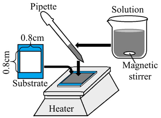
Figure 1.
Apparatus of the drop–dry deposition method.
2. Experimental Section
The deposition solution for the Ni(OH)2 precursor was prepared by dissolving nickel(II) nitrate hexahydrate (Ni(NO3)2·6H2O, minimum 98% purity, Kanto Chemical Co. Inc., Tokyo, Japan) and sodium hydroxide (NaOH, minimum 97% purity, Kanto Chemical Co. Inc., Tokyo, Japan) in pure water (with a specific resistance of 18.2 MΩcm), and stirring with a magnetic stirrer. The indium–tin–oxide (ITO)-coated glass substrate (1.0 × 3.0 cm2, 10 Ω/sq) was degreased with acetone and washed with pure water, and the deposition area was limited to 0.8 × 0.8 cm2 by masking tape (adhesive strength 0.6 N/20 mm). The masking tape was peeled off after the deposition. A pipette was used to drop 0.05 mL of the solution onto the deposition area each time. The substrate was placed on the heater plate and heated, and the temperature of the heater plate was monitored to maintain it at 60 °C until it was visually observed that water on the substrate was evaporated completely. Next, the substrate was rinsed with pure water and blown with nitrogen gas. The Ni(OH)2 film was deposited by repeating the above steps.
During the drying process (with evaporation of the solvent), the low solubility material first precipitates and is deposited on the substrate, and, then, the high solubility material precipitates. The stability of Ni(OH)2 in water has been investigated [45]. The hydrolysis and condensation reactions are not expected in the aqueous solution, and, thus, gel is not formed. The solubility of Ni(OH)2 is approximately 10−6 M when pH = 12 (NaOH concentration of 10 mM). Thus, with evaporation of water, Ni(OH)2 readily precipitates and is deposited on ITO. Then, NaNO3 precipitates on Ni(OH)2 and is washed away in the rinsing process. The overall reactions can be expressed as follows.
Ni(NO3)2 + 2NaOH = Ni(OH)2 + 2NaNO3
The following conditions are examined to optimize the deposition process:
- series (a): Number of drop–dry cycles: 2, 3, 4, 5 (Ni(NO3)2: 10 mM, NaOH: 15 mM).
- series (b): Ni(NO3)2 concentrations: 5, 10, 15, 20 mM (NaOH: 10 mM, cycles: 2).
- series (c): NaOH concentrations: 10, 15, 17.5, 20 mM (Ni(NO3)2: 10 mM, cycles: 2).
After depositing the thin film, the sample was placed in a tube furnace made of quartz, and an annealing treatment was performed at 400 °C for 1 h in air, resulting in thermal decomposition of Ni(OH)2 to NiO [39].
Ni(OH)2 → NiO + H2O
Figure 2 shows the schematic of the ZnO/NiO heterojunction. The ZnO/NiO heterojunction was fabricated by the following process. First, the NiO film with an area of 0.8 × 0.8 cm2 was fabricated on the ITO substrate by DDD and annealing. Then, a ZnO film was deposited on it by ECD. The deposition area of ZnO was limited to 0.6 × 0.6 cm2 by masking tape placed on the NiO film. The tape was removed after the deposition. The ZnO deposition solution contained 0.1 M zinc nitrate hexahydrate (Zn(NO3)2·6H2O, minimum 99% purity, Kanto Chemical Co. Inc., Tokyo, Japan) and was heated to 60 °C. The deposition time was 10 min, and the current density was −1.5 mA/cm2; the chemical reactions of the deposition are shown in ref. [46]. For the current-density–voltage (J-V) characterization, indium electrodes (0.1 × 0.1 cm2) were fabricated on the heterojunction by vacuum evaporation.
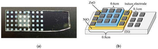
Figure 2.
ZnO/NiO heterojunction: (a) photograph; (b) schematic diagram.
The thickness profiles were measured by an Accretech Surfcom-1400G profilometer. Optical transmittance was measured using a Jasco V-570 UV/VIS/NIR spectrometer. The transmittance data were obtained by dividing the transmittance of the sample by the reference data obtained for the ITO substrate without any deposits. Scanning electron microscope (SEM) images and Auger electron spectroscopy (AES) data were acquired using the JEOL JAMP-9500F field emission microprobe at a probe voltage of 10 keV. Raman spectroscopy measurement was performed using the Jasco NRS-3300 Raman spectroscope with excitation laser wavelength of 532 nm. X-ray diffraction (XRD) data were obtained using the SmartLab SE X-ray diffractometer (Rigaku) with a Cu Kα radiation source. Photoelectrochemical (PEC) measurement was carried out in a three-electrode system with a Ag/AgCl reference electrode. As the electrolyte, 100 mM sodium sulfate (Na2SO4) solution was used. For optical excitation, 100 mW/cm2 light from an ABET technologies 10500 solar simulator was irradiated intermittently at 5 s intervals, and the sample potential was swept within a range from −1 to 0 V and 0 to 1 V with a scanning rate of 5 mV/s.
3. Results and Discussion
3.1. Deposition Conditions
Figure 3 shows an example of the thickness profile obtained to analyze the film thickness and roughness. Figure 4 shows the thicknesses of the samples deposited under different deposition conditions. Figure 4a shows the dependence of the film thickness on the cycle numbers (series (a)). It can be seen from the figure that the film thickness increases from 0.3 μm to 0.75 μm when the number of drop–dry cycles changes from two to three. However, the thickness did not continue to increase after the fourth cycle, and the surface of the sample became hazy, with an increasing nonuniformity. When the cycle number was increased to five, the film cracked and partly peeled off, and the thickness decreased instead. This shows that the thickness of the Ni(OH)2 films obtained by DDD is limited to below 0.75 μm.
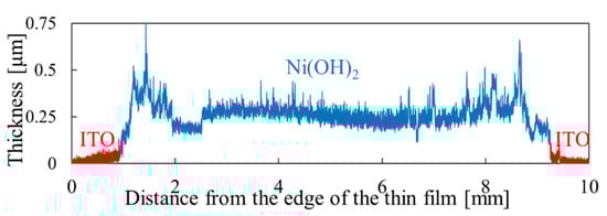
Figure 3.
Thickness profile measurement results for the Ni(OH)2 thin film. (Ni(NO3)2 10 mM, NaOH 15 mM, two deposition cycles).
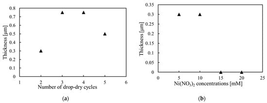
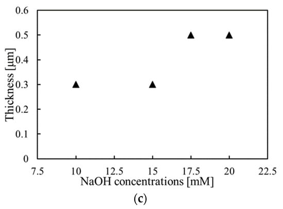
Figure 4.
Film thickness under different deposition conditions: (a) change in the number of depositions; (b) change in Ni(NO3)2 concentration; (c) change in NaOH concentration.
Figure 4b shows the film thickness obtained with different Ni(NO3)2 concentrations (series (b)). With the increase in Ni(NO3)2 concentration (5–20 mM), the ratio of Ni(NO3)2 to NaOH increased from 1/2 to 2. The thicknesses of the samples obtained with 5 and 10 mM Ni(NO3)2 (the ratios of 1/2 and 1) were approximately 0.3 μm, but the surface was slightly rough for 10 mM Ni(NO3)2. The films were not successfully deposited with 15 and 20 mM Ni(NO3)2 (the ratios of 3/2 and 2), indicating that the Ni(NO3)2-to-NaOH ratio should not be higher than 3/2.
Figure 4c shows the film thickness obtained with different NaOH concentrations (series (c)). The thickness of the samples deposited with 10 and 15 mM NaOH (the Ni(NO3)2-to-NaOH ratio of 1 and 2/3) was approximately 0.3 μm. The sample thickness increased to 0.5 μm for 20 mM NaOH (the ratio of 1/2), but the sample surface became rough. This may be because aggregated Ni(OH)2 particles were formed in the solution and attached to the film surface. This indicates that the Ni(NO3)2 concentration ratio should be larger than 1/2.
The transmittance results are shown in Figure 5 for different deposition cycle numbers. There is no absorption edge in the wavelength range in the figure. With the increase in the cycles from two to four, the film thickness increased from 0.3 to 0.75 μm as shown in Figure 4a, and the transmittance decreased from 90% to 70% in the visible region as shown in Figure 5. The thickness of the sample obtained with five cycles decreased as noted above, and the sample had a high transmittance (>90%) in the visible region. Thus, as the thickness increases, the surface roughness tends to increase and the transmittance tends to decrease. For the other deposition conditions (series (b) and (c)), the transmittance was in a range from 80 to 100%, and it tends to be larger for the thinner samples.
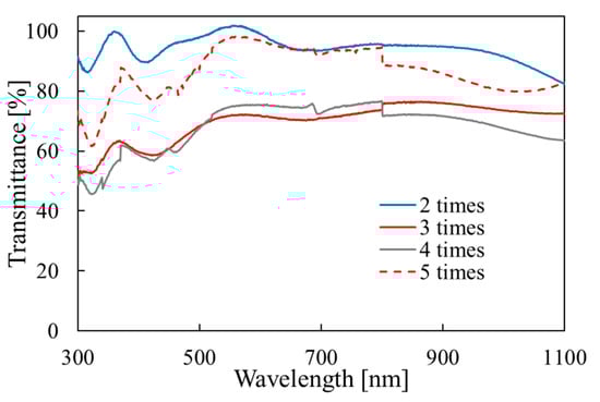
Figure 5.
Optical transmittance for the samples fabricated with different deposition cycle numbers.
In the following characterization, we adopt the deposition condition: 10 mM Ni(NO3)2, 15 mM NaOH and two deposition cycles. Under this condition, the film thickness was approximately 0.3 μm, and the transmittance in the visible light region was 95% or more. In this optimized condition, the ratio of Ni(NO3)2 to NaOH is 2/3, not the stoichiometric ratio of 1/2. When the ratio is 1/2, Ni(OH)2 particle aggregation occurred in the solution, which affects the uniformity of the film. On the other hand, when the concentration ratio of Ni(NO3)2 exceeds 3/2, the deposition of the film failed. Thus, the ratio should be between 1/2 and 3/2, and the ratio of 2/3 was actually selected.
3.2. Characterization of As-Deposited and Annealed Films
By annealing at 400 °C, the thickness was reduced from 0.3 μm to approximately 0.12 μm. This is due to the conversion of Ni(OH)2 to NiO. The theoretical volume change can be calculated using the densities and molar masses of NiO and Ni(OH)2; with the same amount of Ni, the volume of NiO was expected to be 0.48 times that of Ni(OH)2, which is consistent with the experimental results.
The transmittance measurement results before and after annealing are shown in Figure 6. Although the as-deposited Ni(OH)2 film has no absorption edge in the range of the figure, the annealed NiO film has an absorption edge of around 360 nm. Thus, the change from an insulator to a semi-conductor due to annealing was confirmed. Since NiO has a direct bandgap [1], the bandgap was calculated from the plot of (αhν)2 vs. hν, where α is the absorption coefficient and hν is the photon energy. The calculated bandgap is 3.4 eV, which is in the range reported in ref. [1].
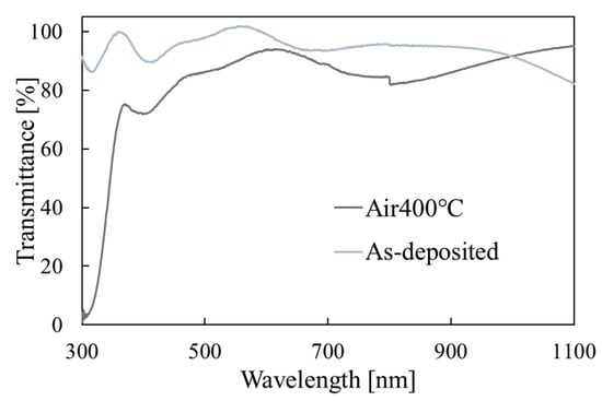
Figure 6.
Optical transmittance measurement results for the films before and after annealing.
Figure 7 shows the SEM images of the thin film. Grain images were not observed on the surfaces, and the film morphology did not change significantly before and after annealing.
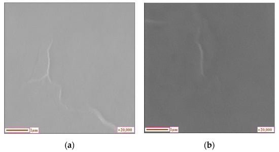
Figure 7.
SEM images of films: (a) as-deposited; (b) annealed at 400 °C for 1 h.
The AES measurement results are shown in Figure 8. Argon ion sputtering was performed for 10 s before the measurement. Only Ni and O were detected before and after annealing. Thus, the other elements in the deposition solution (Na, N) were mostly removed by the rinsing process. The composition ratios O/Ni of the thin film before and after annealing are 1.23 and 1.10, respectively; the oxygen content in the thin film decreased as the thin film changed from Ni(OH)2 to NiO. The argon ion sputtering before the measurement would result in the decomposition of the hydroxide. Thus, the O/Ni composition ratio before annealing was lower than that expected for Ni(OH)2. Similar results have been reported for cobalt hydroxide [44].
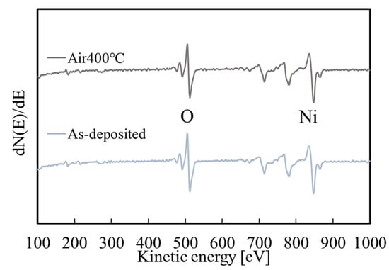
Figure 8.
AES measurement results for the films before and after annealing.
Figure 9 shows the Raman measurement results before and after annealing. The peaks of Ni(OH)2 and ITO (substrate) were observed before annealing [47], and the peaks of NiO and ITO (substrate) were observed after annealing [48]. Thus, it was found that the Ni(OH)2 precursor film was successfully fabricated by DDD, and the film was converted to NiO by annealing.
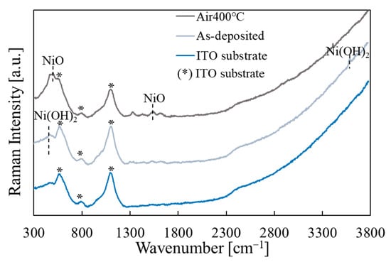
Figure 9.
Raman measurement results for the films before and after annealing. For comparison, the spectrum for the ITO substrate is also shown.
The XRD measurement was performed on the films before and after annealing, and the results are shown in Figure 10a. Only the peaks of ITO were observed for the sample before annealing, whereas the peak corresponding to NiO (1 1 1) was also observed after annealing (JCPDS 04-0835). Thus the annealed film was polycrystalline with clear (1 1 1) preferential orientation. Similar results have been reported for the films deposited by the ECD method [37], while the (2 0 0) peak was also observed for NiO films fabricated by other methods [31,49,50].
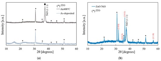
Figure 10.
XRD measurement results: (a) the Ni(OH)2 and NiO films (before and after annealing); (b) the ZnO/NiO heterojunction after annealing (the red indices are for ZnO).
The PEC measurement was performed on the annealed film. The PEC measurement reveals the photo current due to the minority carriers of the semiconductor. The minority carriers of a p-type semiconductor are electrons, and, thus, the photo response will be observed in the negative potential sweep. Conversely, n-type semiconductors respond in the positive potential sweep. The results are shown in Figure 11. The p-type photo response was observed for the annealed thin films, and, therefore, we successfully fabricated p-type NiO thin films by DDD. The photo response was not observed for the Ni(OH)2 precursors.
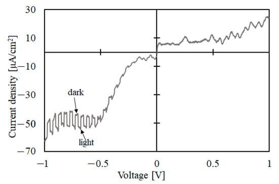
Figure 11.
PEC measurement results of the annealed NiO film.
3.3. ZnO/NiO Heterojunction
Based on the p-type NiO thin film thus prepared, we fabricated a heterojunction with n-type ZnO and measured the optical and electrical properties. Figure 12 shows the thickness measurement result of the heterojunction. The thickness of NiO was approximately 0.2 μm, and the thickness of ZnO prepared by ECD was approximately 0.9 μm.
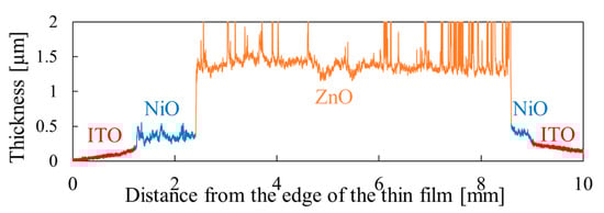
Figure 12.
Thickness profile measurement results for the ZnO/NiO heterojunction.
Figure 13 shows the transmittance of the ZnO/NiO heterojunction and that of the NiO single layer. ZnO has a smaller bandgap than that of NiO, and, thus, the absorption edge in the UV region was red-shifted compared with the spectrum for NiO. The absorption-edge energy of the heterojunction was 3.3 eV, consistent with the literature value for ZnO [46]. The transmittance was more than 70% in the visible range.
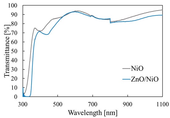
Figure 13.
Optical transmittance measurement results for the ZnO/NiO heterojunction.
The XRD results of the ZnO/NiO heterojunction is shown in Figure 10b. In addition to the peaks of NiO and ITO, the ZnO peaks were also observed (their indices are noted in red in the figure according to JCPDS 36-1451). Thus, the polycrystalline ZnO/NiO heterojunction was successfully prepared.
Figure 14 shows the J-V characteristics of the ZnO/NiO heterojunction. It can be seen that the ZnO/NiO heterojunction exhibits a rectification performance. We repeated the fabrication of the heterojunction, and the rectification properties were observed reproducibly.
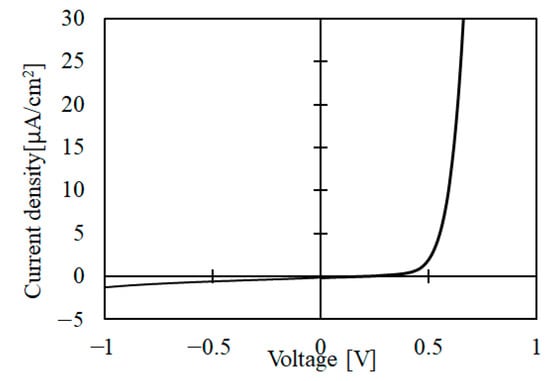
Figure 14.
J-V measurement results of the ZnO/NiO heterojunction.
The successful fabrication of p-type NiO thin films and ZnO/NiO heterojunction demonstrates that the DDD method will be used for the fabrication of NiO-based devices. As mentioned in the introduction, the ZnO/NiO heterojunction has been considered promising for transparent solar cells. Since DDD is so simple, NiO films can be fabricated at a low cost and the solar cell fabrication cost can be reduced. The shortcoming of DDD seems to be the fact that, with an increasing thickness, the thickness uniformity is deteriorated, as discussed in 3.1. Thus, DDD may not be suitable for application where a thick NiO layer is needed. For the ZnO/NiO solar cell application, the NiO layer can be thin since light is mainly absorbed by ZnO, which has a smaller bandgap. A large-area film could be deposited by dropping and spreading the solution from multiple points on the substrate. Thus, DDD would be applicable for the ZnO/NiO solar cells.
As noted in the introduction, the fabrication of ZnO/NiO heterostructure diodes by other chemical solution techniques has been reported [4,10,11,12,13]. The leakage current of the ZnO/NiO cell fabricated in this work seems comparable to those reported previously (of the order of 1 µA/cm2). In some of those previous works, photovoltaic properties were observed, but the output voltage was small, of the order of 10 mV [4,13]. In future studies, we will fabricate a ZnO/NiO solar cell based on DDD-deposited NiO.
4. Conclusions
Ni(OH)2 precursors were prepared by the novel simple technique DDD using an aqueous solution containing Ni(NO3)2 and NaOH, and converted to NiO thin films by annealing. The films were transparent in the visible range. The XRD and Raman peaks of NiO were observed for the annealed films. The results of the PEC measurement showed that the NiO film was p-type and photoconductive. The ZnO/NiO heterojunction was fabricated with ZnO deposited by ECD, and rectification was observed. Thus, NiO films fabricated by DDD can be used for various electronic and electrochemical applications.
Author Contributions
Conceptualization, M.I.; resources, M.I.; supervision, M.I.; investigation, T.O.; writing—original draft preparation, T.L.; writing—review and editing, M.I. All authors have read and agreed to the published version of the manuscript.
Funding
This research received no external funding.
Institutional Review Board Statement
Not applicable.
Informed Consent Statement
Not applicable.
Data Availability Statement
The data is contained within the article.
Conflicts of Interest
The authors declare no conflict of interest.
References
- Karpinski, A.; Ouldhamadouche, N.; Ferrec, A.; Cattin, L.; Richard-Plouet, M.; Brohan, L.; Djouadi, M.A.; Jouan, P.-Y. Optical characterization of transparent nickel oxide films deposited by DC current reactive sputtering. Thin Solid Film. 2011, 519, 5767–5770. [Google Scholar] [CrossRef]
- Hu, L.; Wei, R.H.; Tang, X.W.; Lu, W.J.; Zhu, X.B.; Sun, Y.P. Design strategy for p-type transparent conducting oxides. J. Appl. Phys. 2020, 128, 140902. [Google Scholar] [CrossRef]
- Fioretti, A.N.; Morales-Masis, M. Bridging the p-type transparent conductive materials gap: Synthesis approaches for disperse valence band materials. J. Photon. Energy 2020, 10, 042002. [Google Scholar] [CrossRef]
- Koyama, M.; Ichimura, M. Fabrication of ZnO/NiO transparent solar cells by eleasctrochemical deposition. Jpn. J. Appl. Phys. 2019, 58, 128003. [Google Scholar] [CrossRef]
- Karsthof, R.; Räcke, P.; Wenckstern, H.V.; Grundmann, M. Semi-transparent NiO/ZnO UV photovoltaic cells. Phys. Status Solidi A 2015, 213, 30–37. [Google Scholar] [CrossRef]
- Ohteki, Y.; Sugiyama, M. Electrical properties of ZnO:H films fabricated by RF sputtering deposition and fabrication of p-NiO/n-ZnO heterojunction devices. Jpn. J. Appl. Phys. 2018, 57, 071101. [Google Scholar] [CrossRef]
- Patel, M.; Kima, H.S.; Kim, J.; Yun, J.H.; Kim, S.J.; Choi, E.H.; Park, H.H. Excitonic metal oxide heterojunction (NiO/ZnO) solar cells for all-transparent module integration. Sol. Energy Mater. Sol. Cells 2017, 170, 246–253. [Google Scholar] [CrossRef]
- Hasan, M.R.; Xie, T.; Barron, S.C.; Liu, G.; Nguyen, N.V.; Motayed, A.; Rao, M.V.; Debnath, R. Self-powered p-NiO/n-ZnO heterojunction ultraviolet photodetectors fabricated on plastic substrates. APL Mater. 2015, 3, 106101. [Google Scholar] [CrossRef]
- Kawade, D.; Moriyama, K.; Nakamura, F.; Chichibu, S.F.; Sugiyama, M. Fabrication of visible-light transparent solar cells composed of NiO/NixZn1-xO/ZnO heterostructures. Phys. Status Solidi C 2015, 12, 785–788. [Google Scholar] [CrossRef]
- Kim, D.Y.; Ryu, J.; Manders, J.; Lee, J.; So, F. Air-Stable, Solution-Processed Oxide p–n Heterojunction Ultraviolet Photodetector. ACS Appl. Mater. Interfaces 2014, 6, 1370–1374. [Google Scholar] [CrossRef]
- Xie, T.; Liu, G.; Wen, B.; Ha, J.Y.; Nguyen, N.V.; Motayed, A.; Debnath, R. Tunable Ultraviolet Photoresponse in Solution-Processed p–n Junction Photodiodes Based on Transition-Metal Oxides. ACS Appl. Mater. Interfaces 2015, 7, 9660–9667. [Google Scholar] [CrossRef] [PubMed]
- Abbasi, M.A.; Ibupoto, Z.H.; Khan, A.; Nur, O.; Willander, M. Fabrication of UV photo-detector based on coral reef like p-NiO/n-ZnO nanocomposite structures. Mater. Lett. 2013, 108, 149–152. [Google Scholar] [CrossRef]
- Shen, Y.; Yan, X.; Bai, Z.; Zheng, X.; Sun, Y.; Liu, Y.; Lin, P.; Chen, X.; Zhang, Y. A self-powered ultraviolet photodetector based on solution-processed p-NiO/n-ZnO nanorod array heterojunction. RSC Adv. 2015, 5, 5976–5981. [Google Scholar] [CrossRef]
- Hu, C.; Chu, K.; Zhao, Y.; Teoh, W.Y. Efficient Photoelectrochemical Water Splitting over Anodized p-Type NiO Porous Films. ACS Appl. Mater. Interfaces 2014, 6, 18558–18568. [Google Scholar] [CrossRef]
- Al-Akraa, I.M.; Asal, Y.M.; Khamis, S.D. Assembling of NiOx/MWCNTs-GC Anodic Nanocatalyst for Water Electrolysis Applications. Int. J. Electrochem. Sci. 2018, 13, 9712–9720. [Google Scholar] [CrossRef]
- Rajendran, R.; Yaakob, Z.; Teridi, M.A.M.; Rahamana, M.S.A.; Sopian, K. Preparation of nanostructured p-NiO/n-Fe2O3 heterojunction and study of their enhanced photoelectrochemical water splitting performance. Mater. Lett. 2014, 133, 123–126. [Google Scholar] [CrossRef]
- Baraik, K.; Singh, S.D.; Kumar, Y.; Ajimsha, R.S.; Misra, P.; Jha, S.N.; Ganguli, T. Epitaxial growth and band alignment properties of NiO/GaN heterojunction for light emitting diode applications. Appl. Phys. Lett. 2017, 110, 191603. [Google Scholar] [CrossRef]
- Zhou, F.; Gong, H.; Xu, W.; Yu, X.; Xu, Y.; Yang, Y.; Ren, F.; Gu, S.; Zheng, Y.; Zhang, R.; et al. 1.95-kV Beveled-Mesa NiO/β-Ga2O3 Heterojunction Diode With 98.5% Conversion Efficiency and Over Million-Times Overvoltage Ruggedness. IEEE Trans. Power Electron. 2022, 37, 1223–1227. [Google Scholar] [CrossRef]
- Bai, S.; Han, J.; Han, N.; Zhang, K.; Sun, J.; Sun, L.; Luo, R.; Li, D.; Chen, A. An α-Fe2O3/NiO p–n hierarchical heterojunction for the sensitive detection of trimethylamine. Inorg. Chem. Front. 2020, 7, 1532–1539. [Google Scholar] [CrossRef]
- Hotovy, I.; Rehacek, V.; Siciliano, P.; Capone, S.; Spiess, L. Sensing characteristics of NiO thin films as NO2 gas sensor. Thin Solid Film. 2002, 418, 9–15. [Google Scholar] [CrossRef]
- Bandara, J.; Weerasinghe, H. Solid-state dye-sensitized solar cell with p-type NiO as a hole collector. Sol. Energy Mater. Sol. Cells 2005, 85, 385–390. [Google Scholar] [CrossRef]
- Nakasa, A.; Usami, H.; Sumikura, S.; Hasegawa, S.; Koyama, T.; Suzuki, E. High Voltage Dye-sensitized Solar Cell using a Nanoporous NiO Photocathode. Chem. Lett. 2005, 34, 500–501. [Google Scholar] [CrossRef]
- Islam, M.B.; Yanagida, M.; Shirai, Y.; Nabetani, Y.; Miyano, K. NiOx Hole Transport Layer for Perovskite Solar Cells with Improved Stability and Reproducibility. ACS Omega 2017, 2, 2291–2299. [Google Scholar] [CrossRef] [Green Version]
- Yan, Q.; Gong, H.; Zhou, H.; Zhang, J.; Ye, J.; Liu, Z.; Wang, C.; Zheng, X.; Zhang, R.; Hao, Y. Low density of interface trap states and temperature dependence study of Ga2O3 Schottky barrier diode with p-NiOx termination. Appl. Phys. Lett. 2022, 120, 092106. [Google Scholar] [CrossRef]
- Kuanr, S.K.; Babu, K.S. Structural and growth aspects of electron beam physical vapor deposited NiO-CeO2 nanocomposite films. J. Vac. Sci. Technol. A 2016, 34, 021507. [Google Scholar] [CrossRef]
- Salazar, P.; Rico, V.; González-Elipe, A.R. Non-enzymatic hydrogen peroxide detection at NiO nanoporous thin film-electrodes prepared by physical vapor deposition at oblique angles. Electrochim. Acta 2017, 235, 534–542. [Google Scholar] [CrossRef]
- Sato, H.; Minami, T.; Takata, S.; Yamada, T. Transparent conducting p-type NiO thin films prepared by magnetron sputtering. Thin Solid Films 1993, 236, 27–31. [Google Scholar] [CrossRef]
- Usha, K.S.; Sivakumar, R.; Sanjeeviraja, C. Optical constants and dispersion energy parameters of NiO thin films prepared by radio frequency magnetron sputtering technique. J. Appl. Phys. 2013, 114, 123501. [Google Scholar] [CrossRef]
- Reddy, A.M.; Reddy, A.S.; Lee, K.S.; Reddy, P.S. Growth and characterization of NiO thin films prepared by dc reactive magnetron sputtering. Solid State Sci. 2011, 13, 314–320. [Google Scholar] [CrossRef]
- Patil, P.S.; Kadam, L.D. Preparation and characterization of spray pyrolyzed nickel oxide (NiO) thin films. Appl. Surf. Sci. 2002, 199, 211–221. [Google Scholar] [CrossRef]
- Reguig, B.A.; Khelil, A.; Cattin, L.; Morsli, M.; Bernède, J.C. Properties of NiO thin films deposited by intermittent spray pyrolysis process. Appl. Surf. Sci. 2007, 253, 4330–4334. [Google Scholar] [CrossRef]
- Cattin, L.; Reguig, B.A.; Khelil, A.; Morsli, M.; Benchouk, K.; Bernède, J.C. Properties of NiO thin films deposited by chemical spray pyrolysis using different precursor solutions. Appl. Surf. Sci. 2008, 254, 5814–5821. [Google Scholar] [CrossRef]
- Zorkipli, N.N.M.; Kaus, N.H.M.; Mohamad, A.A. Synthesis of NiO Nanoparticles through Sol-gel Method. Procedia Chem. 2016, 19, 626–631. [Google Scholar] [CrossRef] [Green Version]
- Yang, Q.; Sha, J.; Ma, X.; Yang, D. Synthesis of NiO nanowires by a sol-gel process. Mater. Lett. 2005, 59, 1967–1970. [Google Scholar] [CrossRef]
- Teoh, L.G.; Li, K.D. Synthesis and Characterization of NiO Nanoparticles by Sol–Gel Method. Mater. Trans. 2012, 53, 2135–2140. [Google Scholar] [CrossRef] [Green Version]
- Ivanova, T.; Harizanova, A.; Shipochka, M.; Vitanov, P. Nickel Oxide Films Deposited by Sol-Gel Method: Effect of Annealing Temperature on Structural, Optical, and Electrical Properties. Materials 2022, 15, 1742. [Google Scholar] [CrossRef]
- Koyama, M.; Ichimura, M. Fast electrochemical deposition of Ni(OH)2 precursor involving water electrolysis for fabrication of NiO thin films. Semicond. Sci. Technol. 2018, 33, 055011. [Google Scholar] [CrossRef]
- Zhao, L.; Su, G.; Liu, W.; Cao, L.; Wang, J.; Dong, Z.; Song, M. Optical and electrochemical properties of Cu-doped NiO films prepared by electrochemical deposition. Appl. Surf. Sci. 2011, 257, 3974–3979. [Google Scholar] [CrossRef]
- Srinivasan, V.; Weidner, J.W. An Electrochemical Route for Making Porous Nickel Oxide Electrochemical Capacitors. J. Electrochem. Soc. 1997, 144, L210–L213. [Google Scholar] [CrossRef]
- Nam, K.W.; Kim, K.B. A Study of the Preparation of NiOx Electrode via Electrochemical Route for Supercapacitor Applications and Their Charge Storage Mechanism. J. Electrochem. Soc. 2002, 149, A346–A354. [Google Scholar] [CrossRef]
- Liu, Y.; Li, G.; Mi, R.; Deng, C.; Gao, P. An environment-benign method for the synthesis of p-NiO/n-ZnO heterostructure with excellent performance for gas sensing and photocatalysis. Sens. Actuators B Chem. 2014, 191, 537–544. [Google Scholar] [CrossRef]
- Hall, D.S.; Lockwood, D.J.; Bock, C.; MacDougall, B.R. Nickel hydroxides and related materials: A review of their structures, synthesis and properties. Proc. R. Soc. A 2015, 471, 20140792. [Google Scholar] [CrossRef] [PubMed]
- Li, T.; Ichimura, M. Fabrication of Transparent Mg(OH)2 Thin Films by Drop-Dry Deposition. Materials 2021, 14, 724. [Google Scholar] [CrossRef] [PubMed]
- Li, T.; Ichimura, M. Drop-dry deposition of Co3O4 and fabrication of heterojunction solar cells with electrochemically deposited ZnO. Semicond. Sci. Technol. 2021, 36, 095030. [Google Scholar] [CrossRef]
- Pourbaix, M. Atlas of Electrochemical Equilibria in Aqueous Solutions, 2nd ed.; National Association of Corrosion Engineers: Houston, TX, USA, 1974; p. 336. [Google Scholar]
- Izaki, M.; Omi, T. Electrolyte Optimization for Cathodic Growth of Zinc Oxide Films. J. Electrochem. Soc. 1996, 143, L53–L55. [Google Scholar] [CrossRef]
- Bernard, M.C.; Keddam, M.; Takenouti, H.; Bernard, P.; Sényarich, S. Electrochemical Behavior of Quasi-Spherical β - Ni(OH)2 Particles Studied by Roman Spectroscopy. J. Electrochem. Soc. 1996, 143, 2447. [Google Scholar] [CrossRef]
- Dietz, R.E.; Parisot, G.I.; Meixner, A.E. Infrared Absorption and Raman Scattering by Two-Magnon Processes in NiO. Phys. Rev. B 1971, 4, 2302–2310. [Google Scholar] [CrossRef]
- Kang, J.K.; Rhee, S.W. Chemical vapor deposition of nickel oxide films from Ni(C5H5)2/O2. Thin Solid Film. 2001, 391, 57–61. [Google Scholar] [CrossRef]
- Chen, H.L.; Lu, Y.M.; Hwang, W.S. Effect of Film Thickness on Structural and Electrical Properties of Sputter-Deposited Nickel Oxide Films. Mater. Trans. 2005, 46, 872–879. [Google Scholar] [CrossRef] [Green Version]
Publisher’s Note: MDPI stays neutral with regard to jurisdictional claims in published maps and institutional affiliations. |
© 2022 by the authors. Licensee MDPI, Basel, Switzerland. This article is an open access article distributed under the terms and conditions of the Creative Commons Attribution (CC BY) license (https://creativecommons.org/licenses/by/4.0/).