
Characterization and Programming Algorithm of Phase Change Memory Cells for Analog In-Memory Computing

 ,
,  ,
,
Abstract
1. Introduction
- Noise: low-frequency (flicker) noise affects cells behavior, as random electron traps are located in the cell lattice, especially in the amorphous region.
- Time drift: cell conductance tends to decrease due to amorphization and relaxation phenomena of the crystal lattice.
- Uncertainty of the initial conductance value: different cells respond differently to the same programming pulses. Moreover, the response of the same cell to subsequent programming cycles shows a large variability. This leads to dispersion and inaccuracy of the conductance levels.
2. Material and Methods
2.1. PCM Test Chip and Evaluation Board
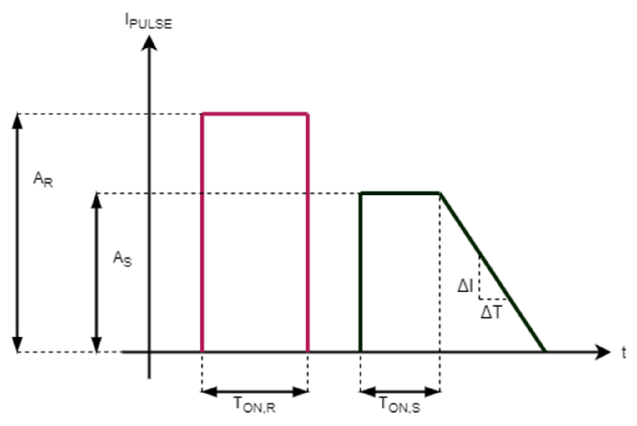
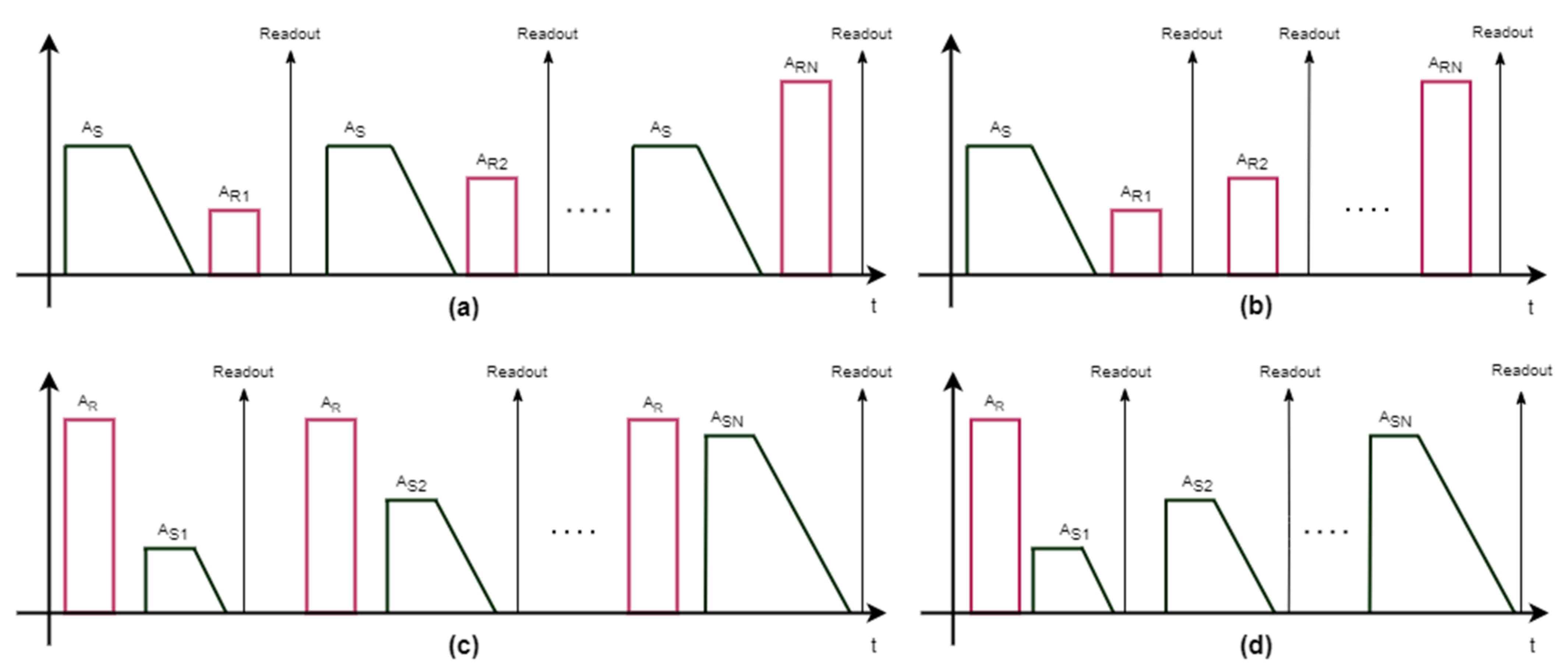
2.2. Programming Pulses Parameters
- a SET pulse is a trapezoidal current pulse, composed of an initial melting phase, followed by a slow crystallization phase;
- a RESET pulse consists in a higher current flow and it is applied in order to melt the central portion of the cell. The molten material quenches into the amorphous phase, producing a cell in the high-resistance state.
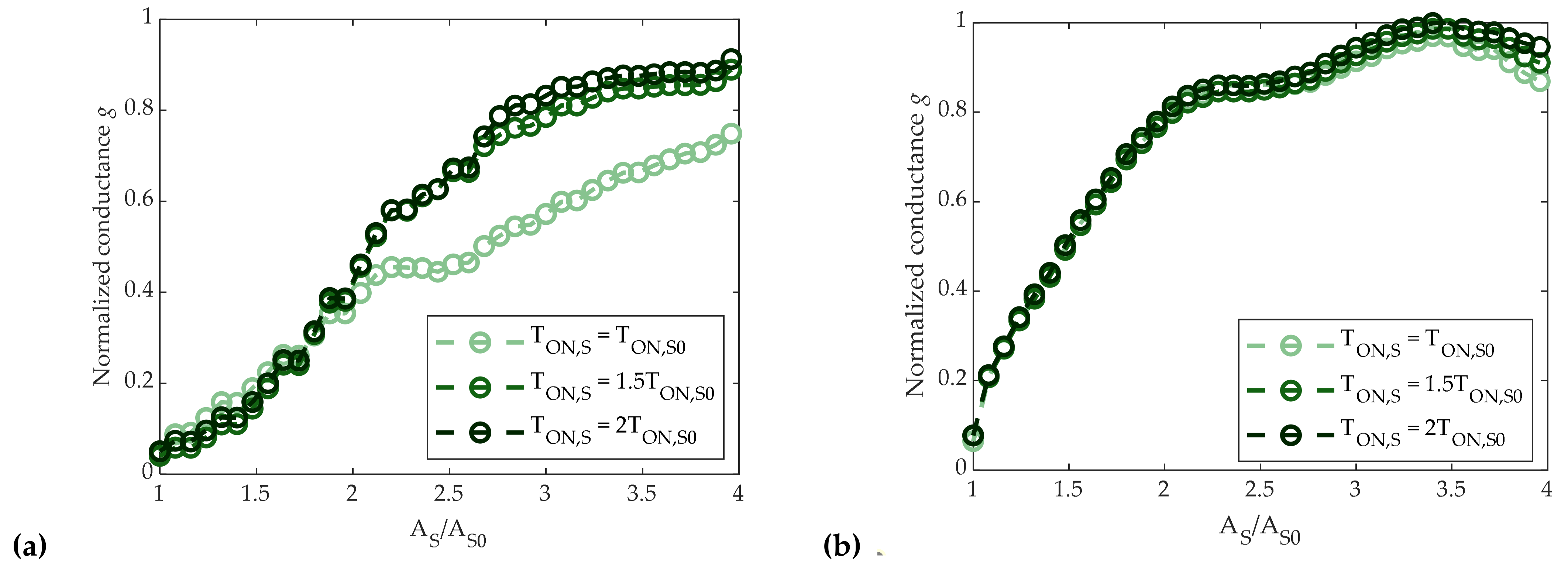
- the SET pulse can be modulated in amplitude (AS), width of the flat portion (TON,S), and decaying slope (ΔI/ΔT);
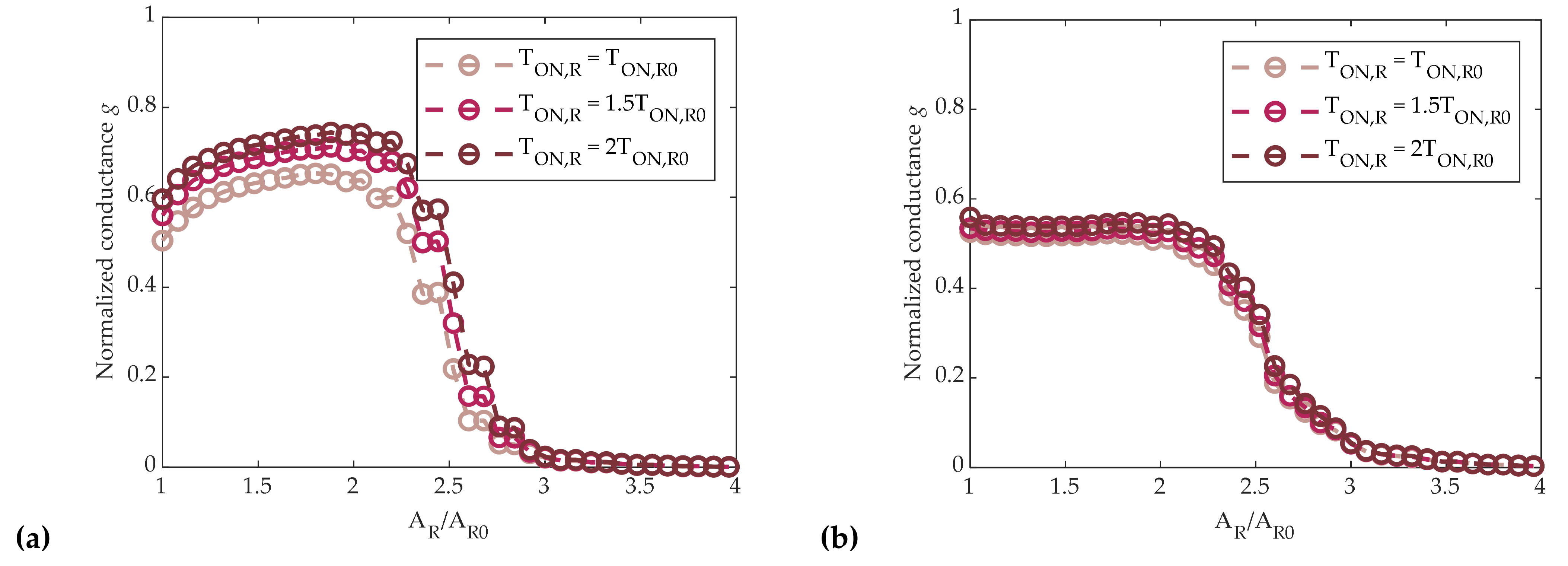
- the RESET pulse can be modulated in amplitude (AR) and width TON,R.
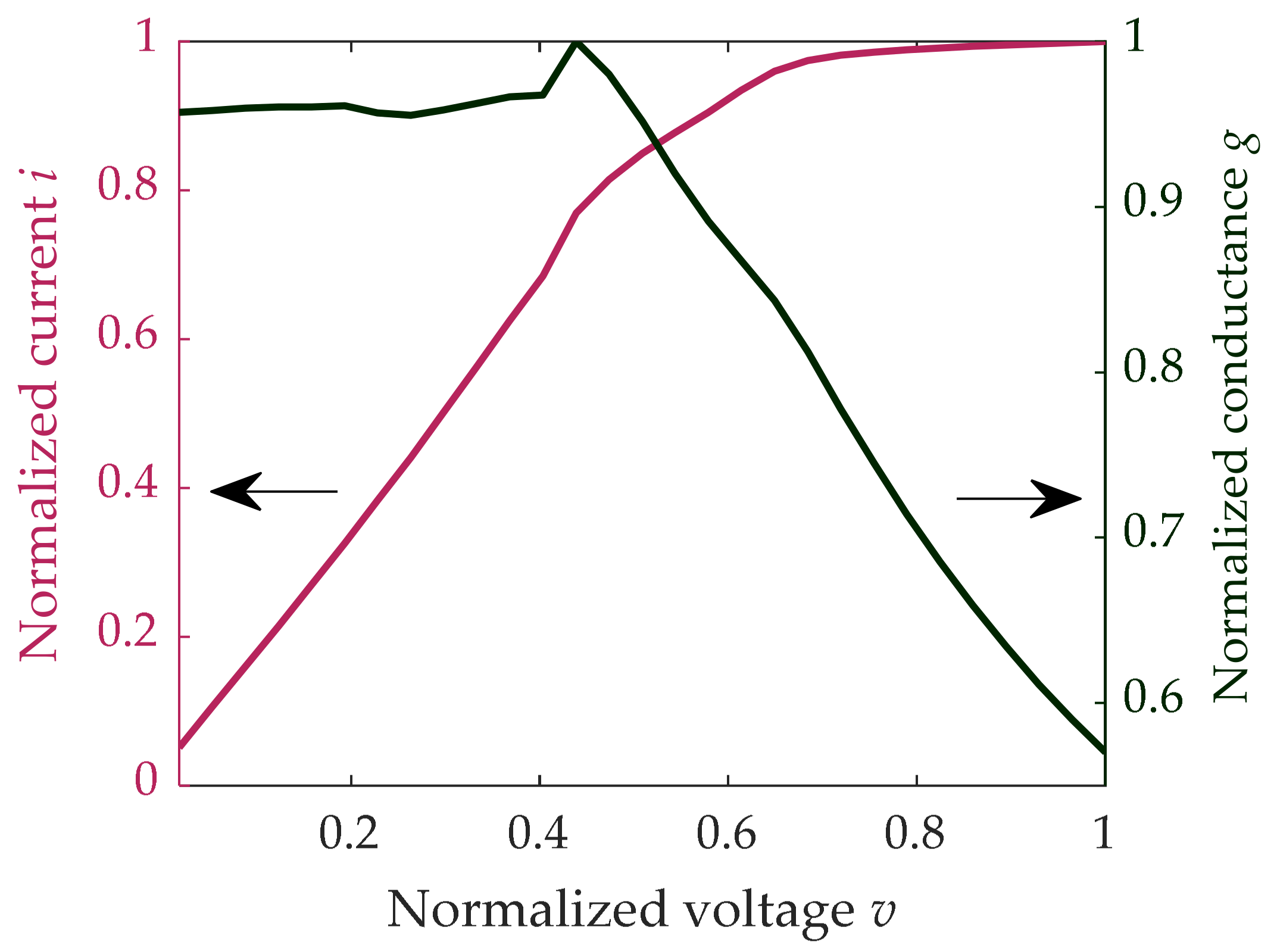
2.3. Readout Voltage Choice
3. Results and Discussion
3.1. PCM Cell Characterization Using Single-SET Pulses
3.1.1. Noise
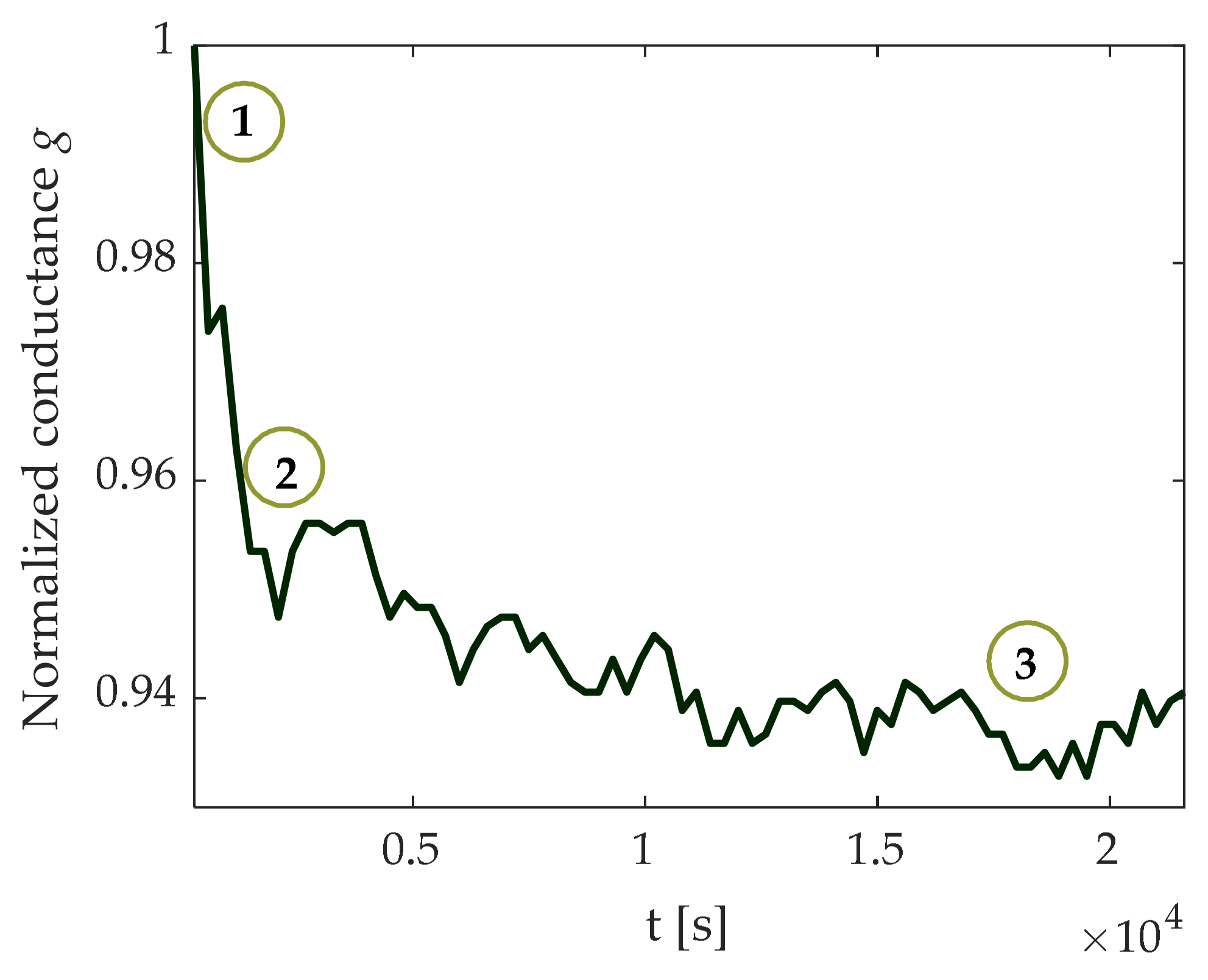
3.1.2. Time Drift
3.2. PCM Cell Characterization Using Multiple Pulses
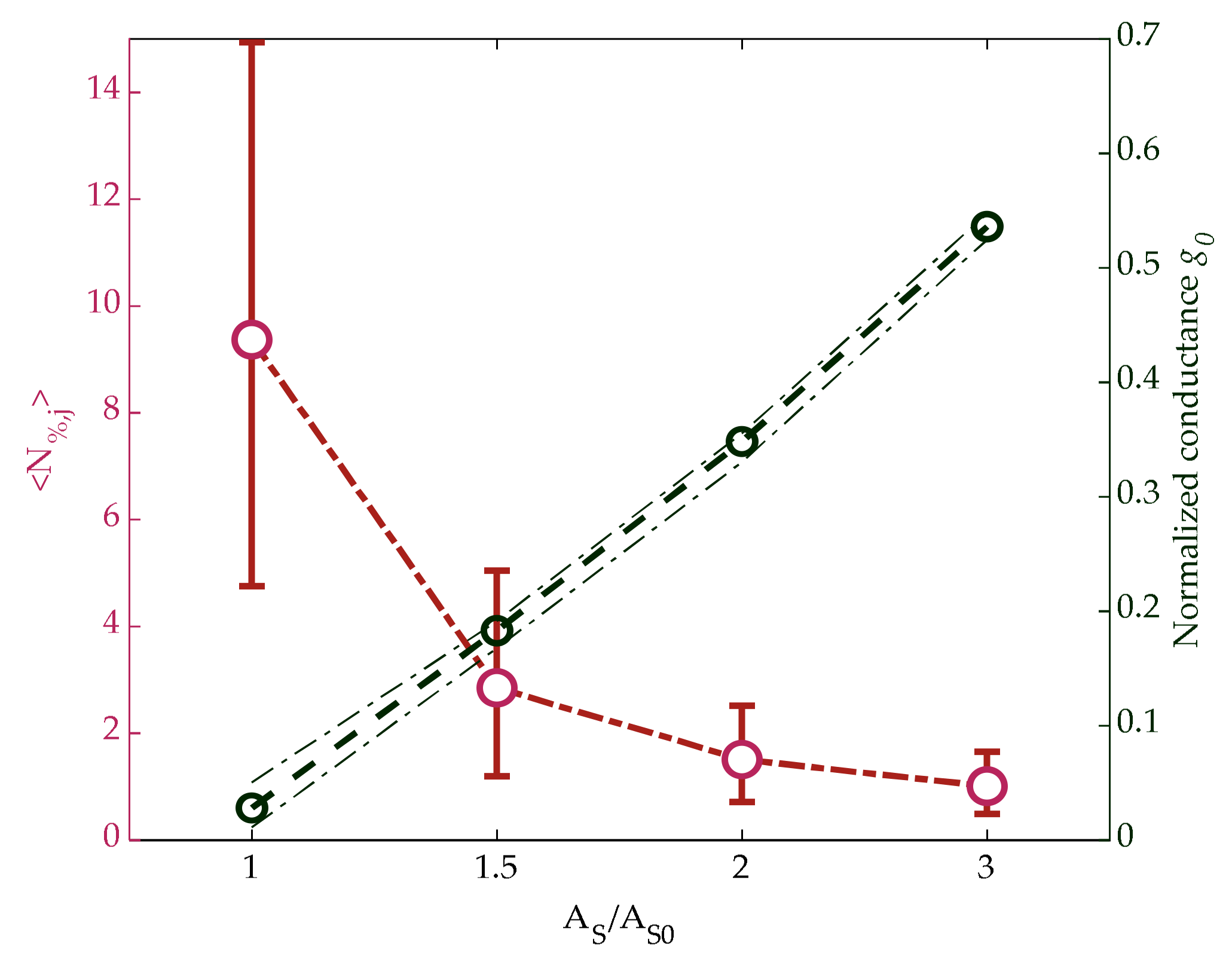
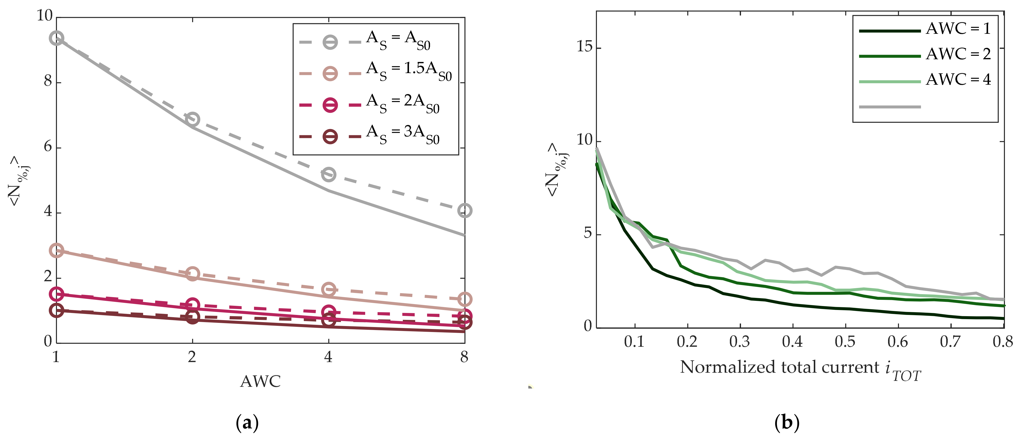
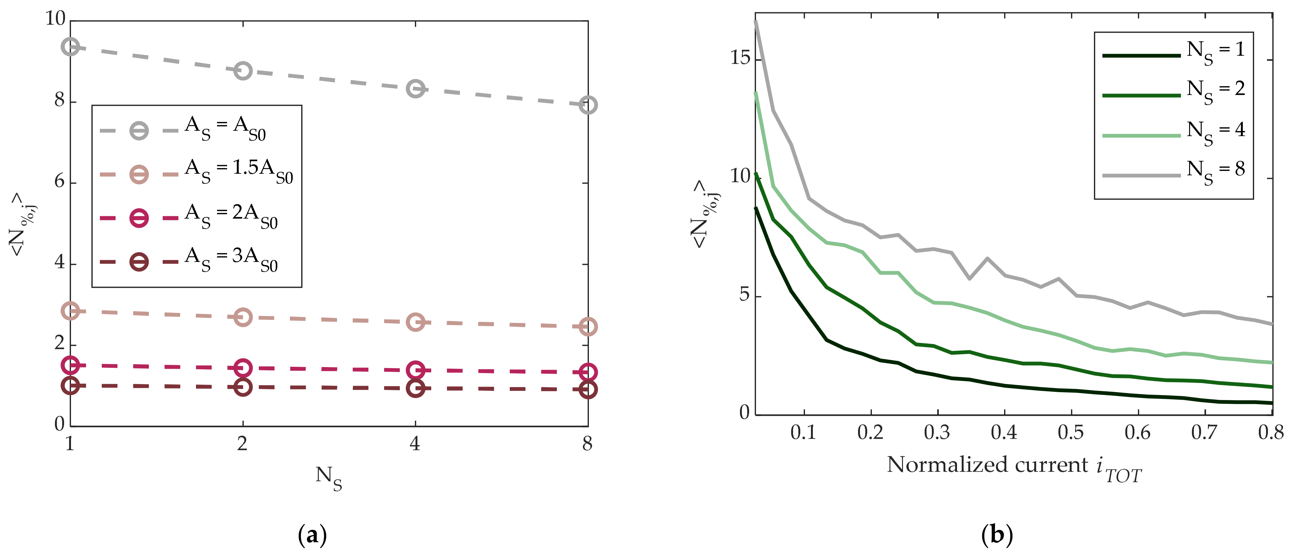
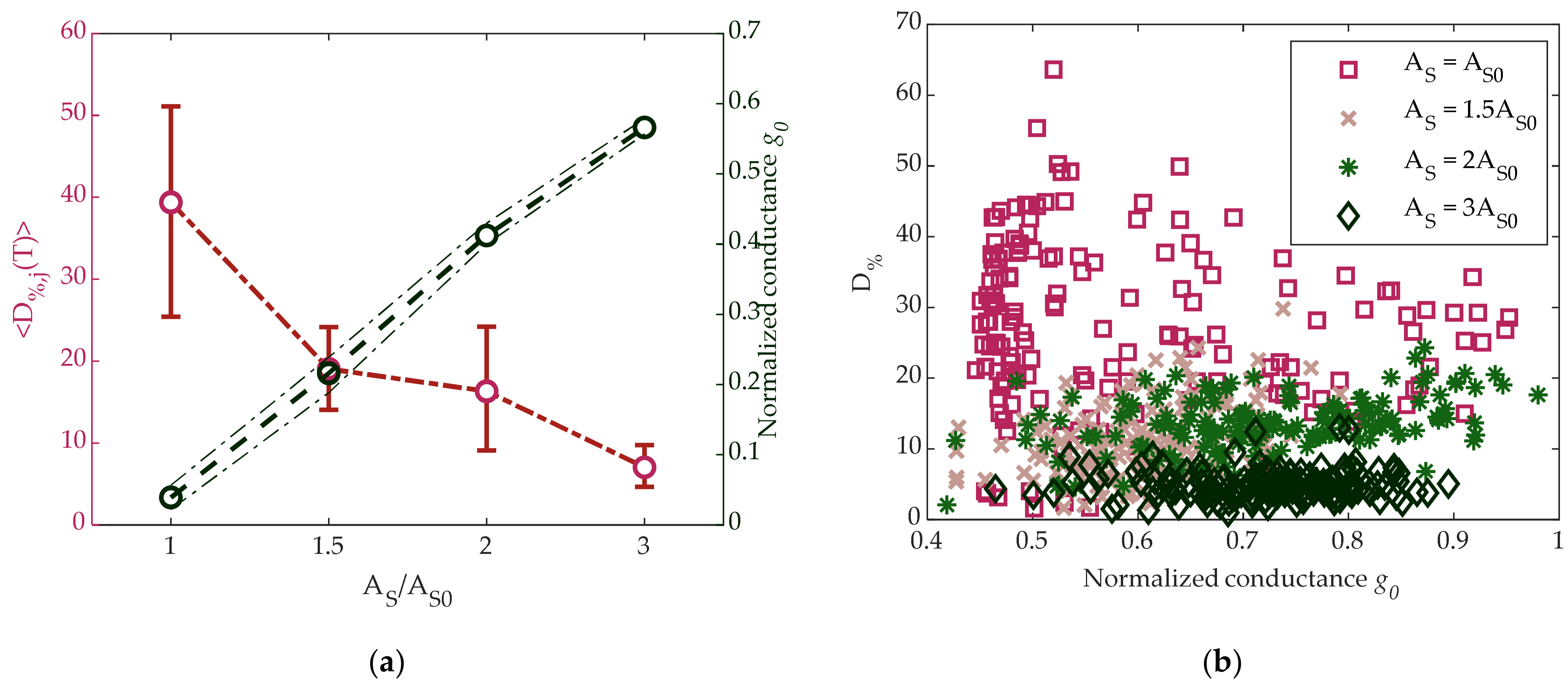
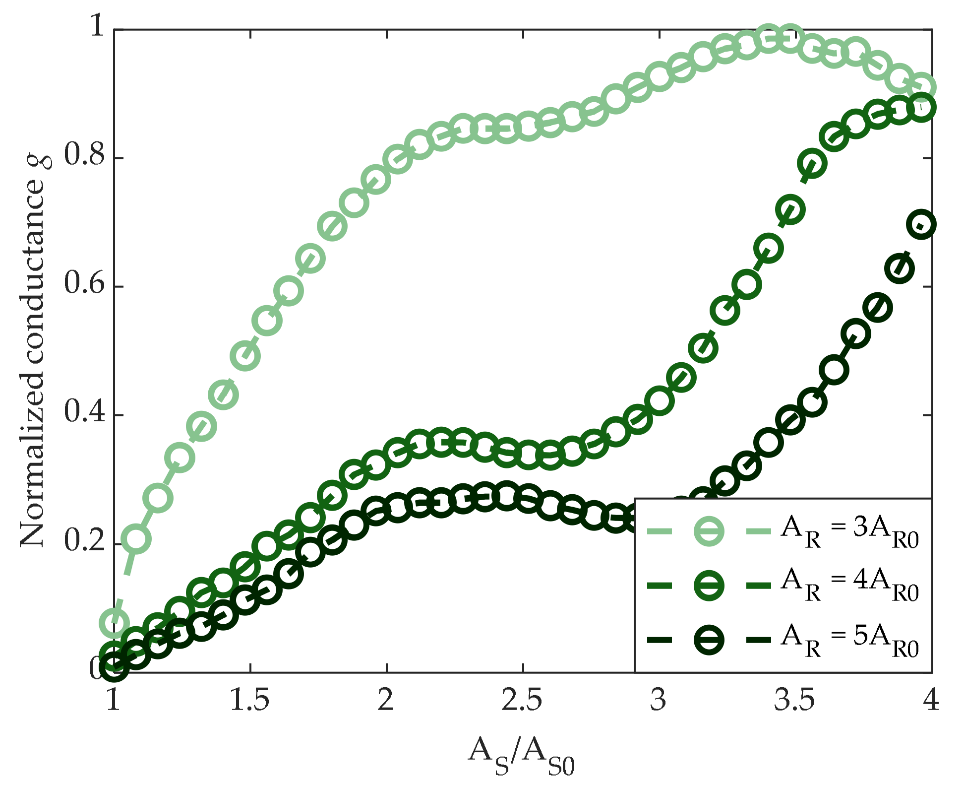
3.2.1. Conductance Tunability
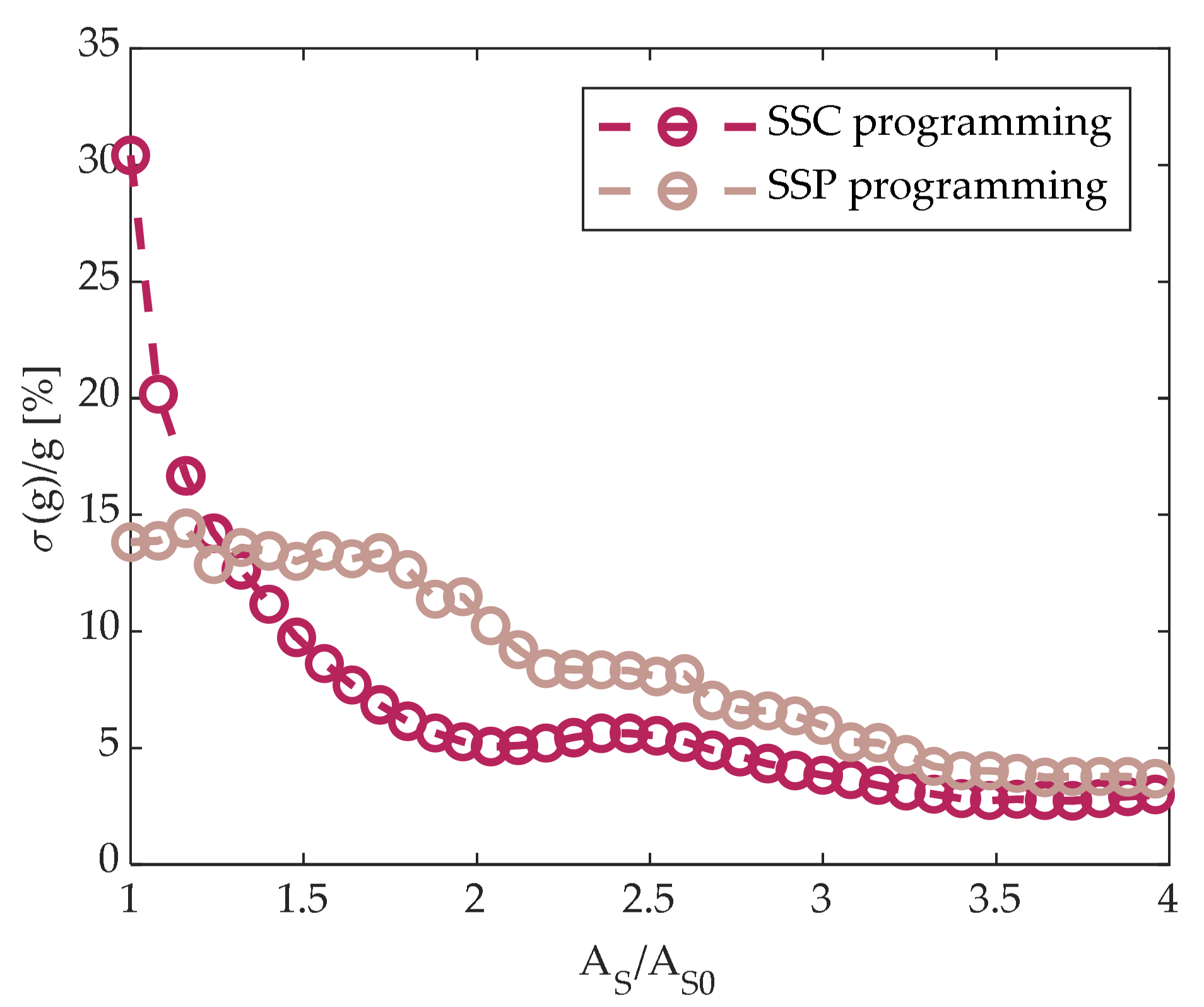
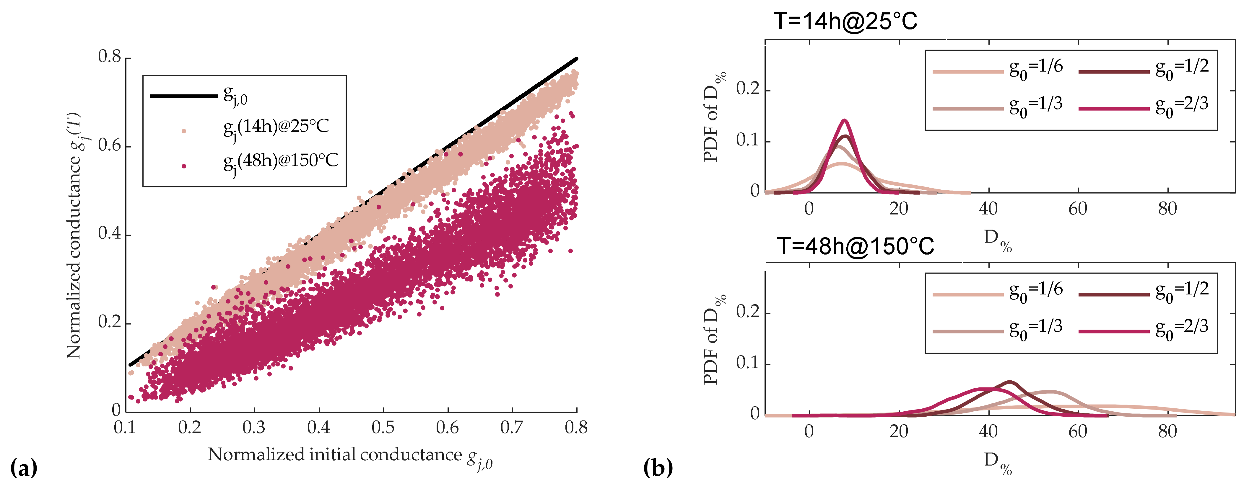
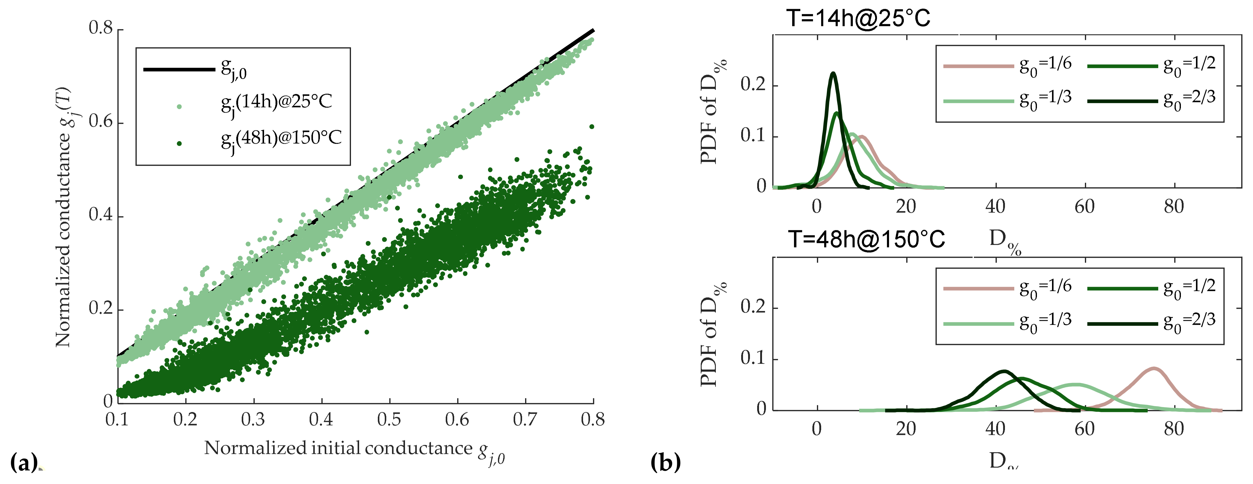
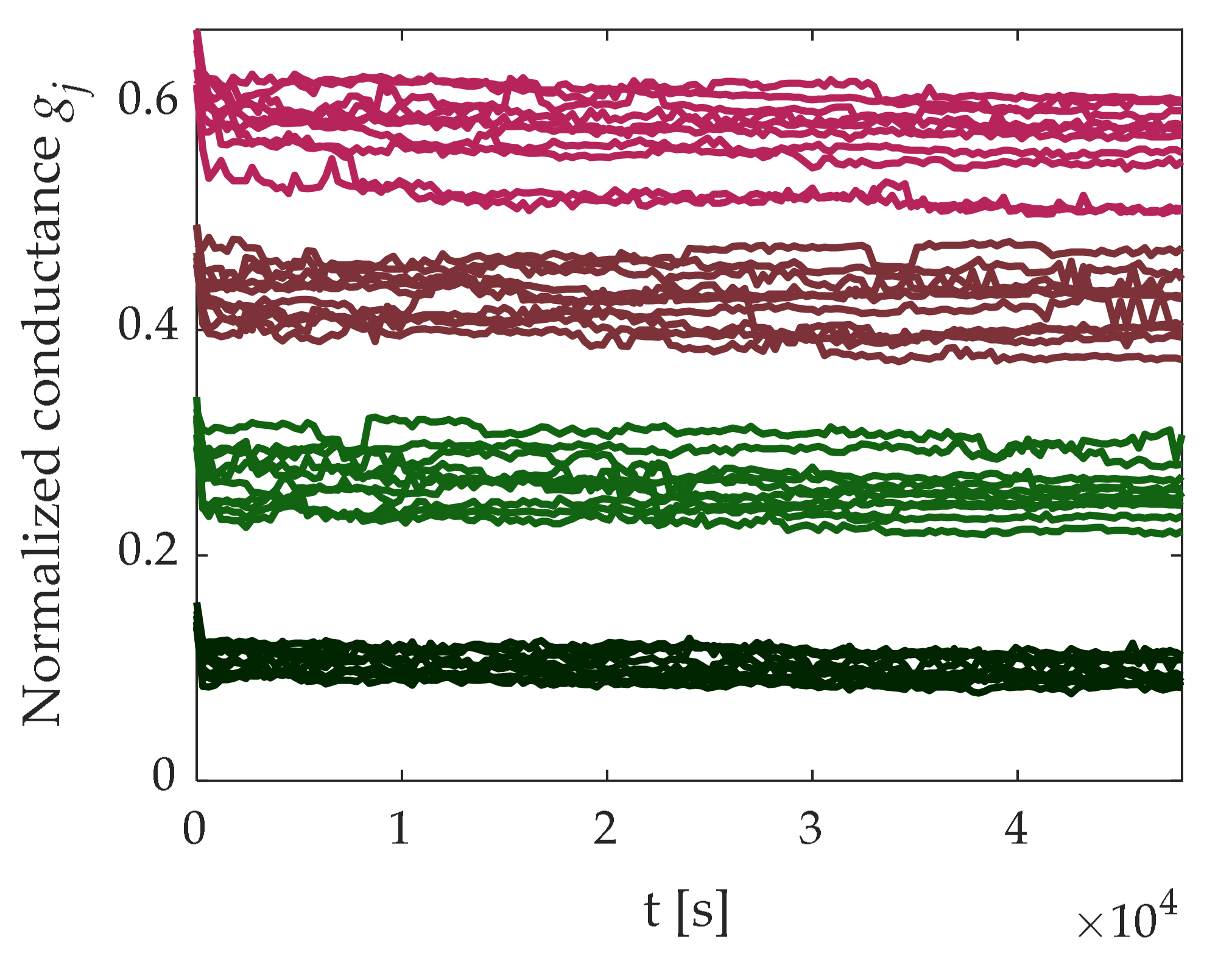
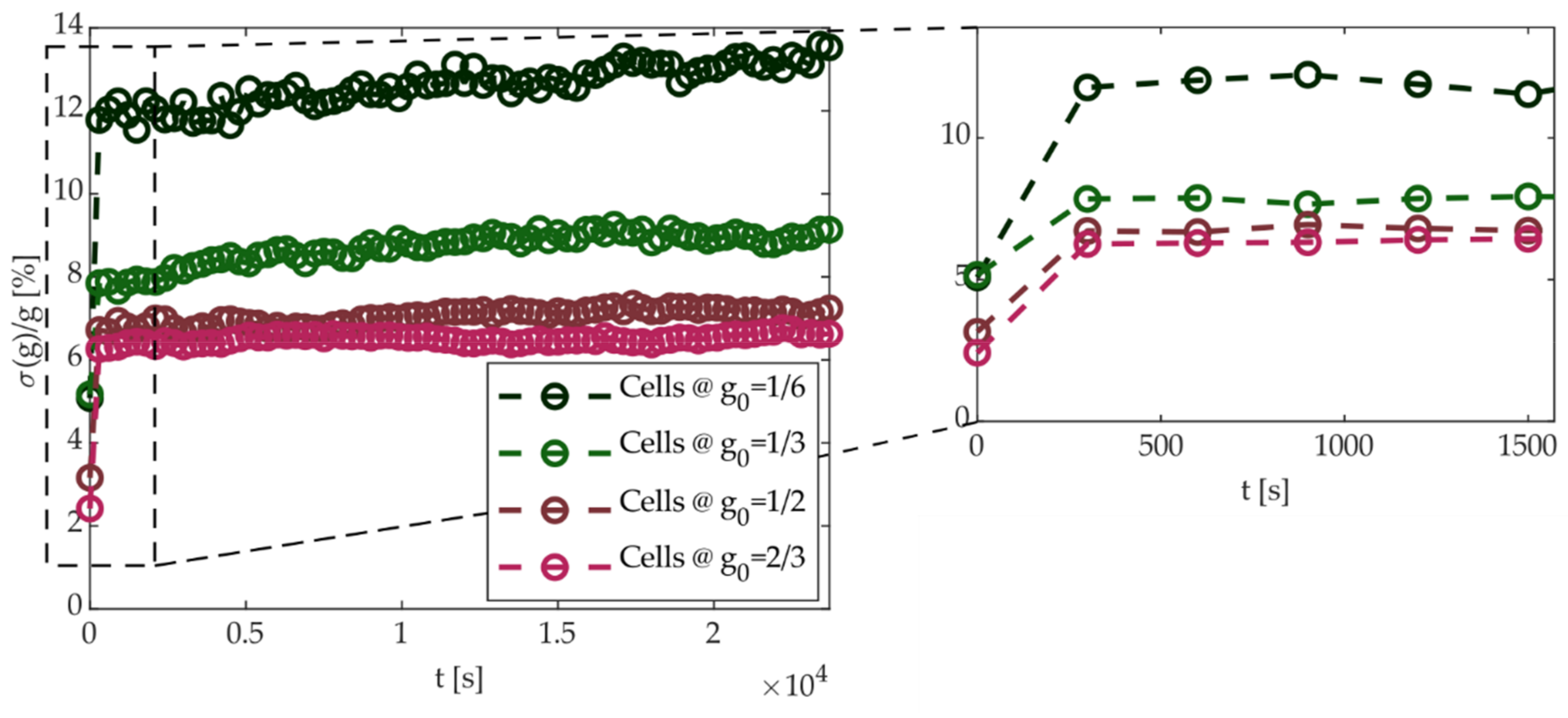
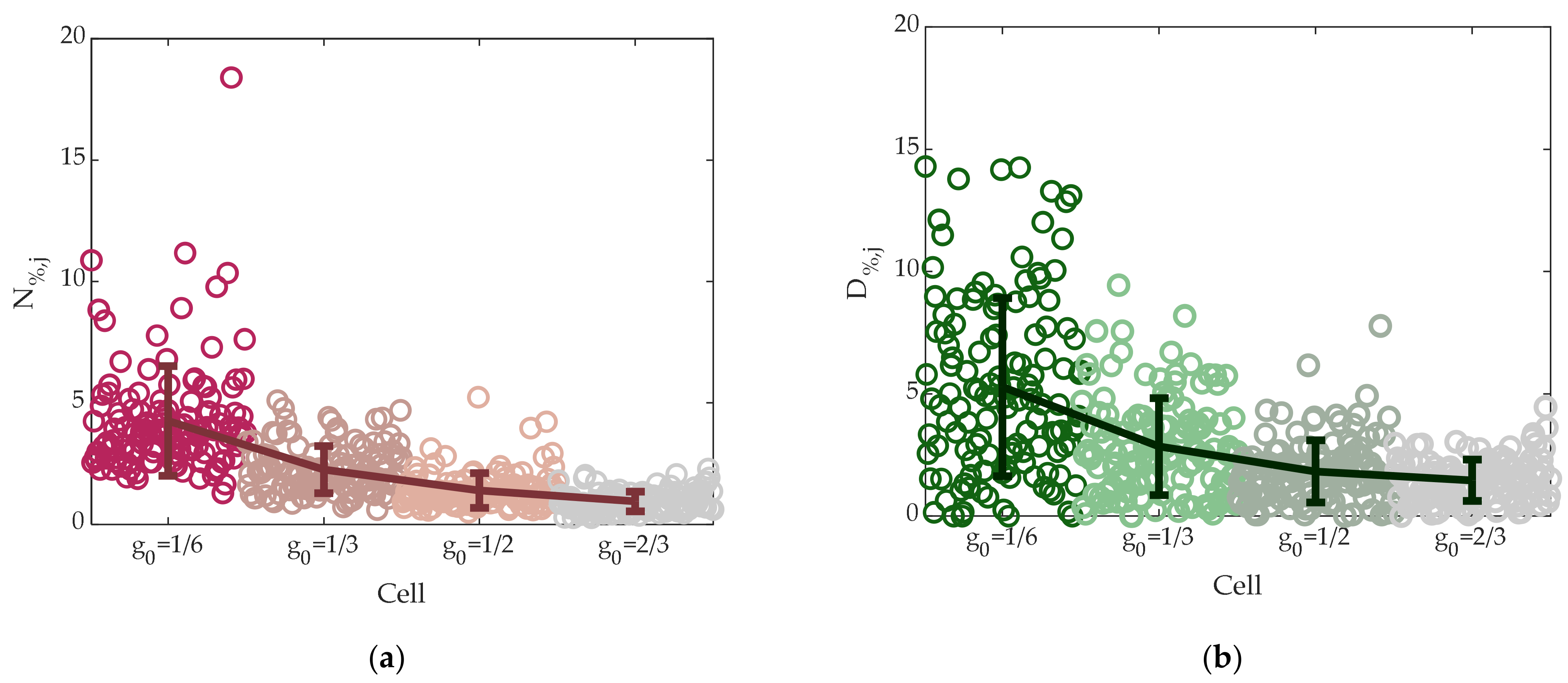
3.2.2. Drift-Induced Dispersion
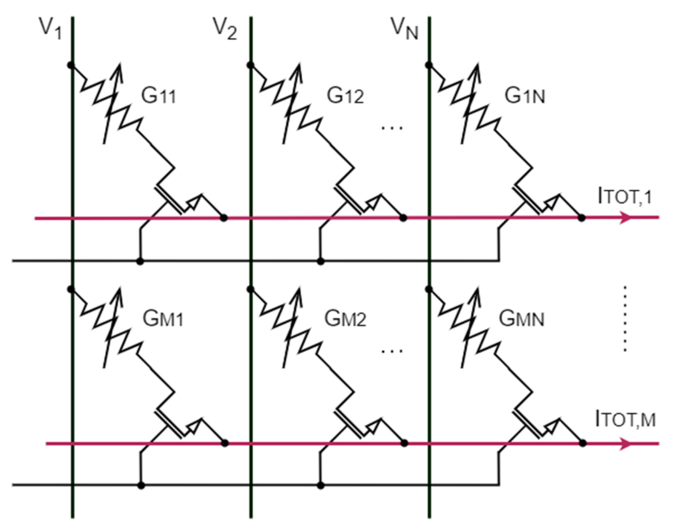
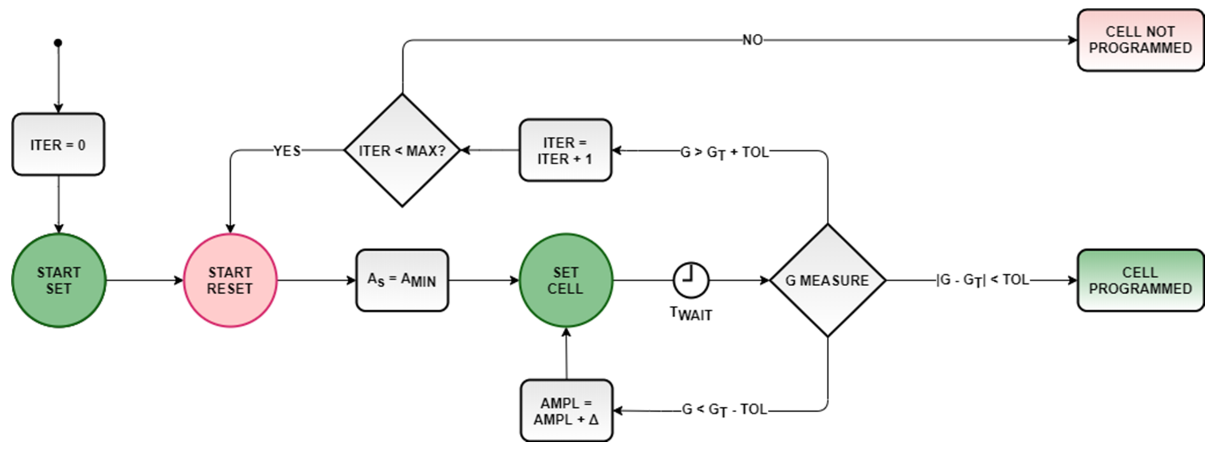
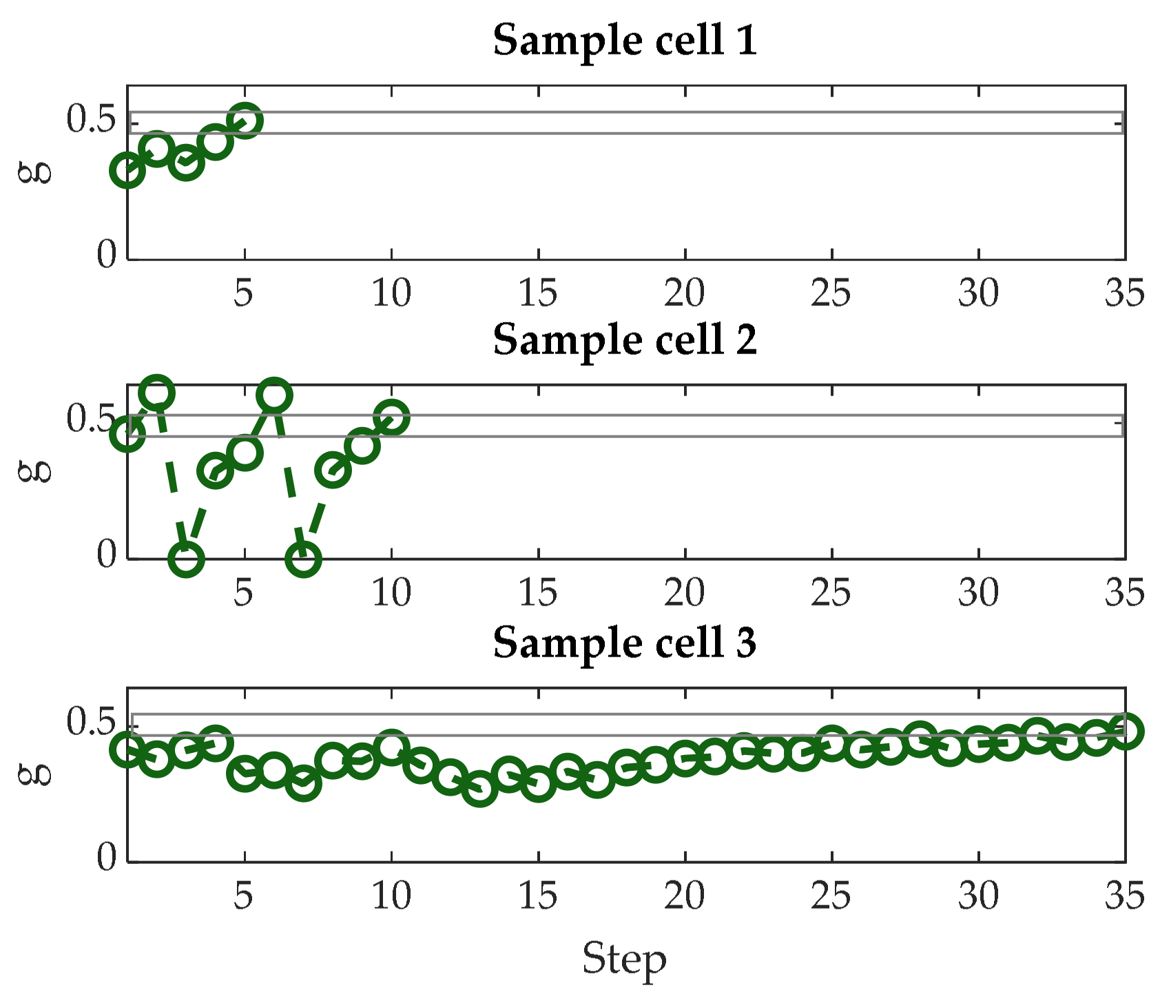
4. A Programming Algorithm for AIMC
5. Conclusions
Author Contributions
Funding
Institutional Review Board Statement
Conflicts of Interest
References
- Burr, G.W.; Kurdi, B.N.; Scott, J.C.; Lam, C.H.; Gopalakrishnan, K.; Shenoy, R.S. Overview of candidate device technologies for storage-class memory. IBM J. Res. Dev. 2008, 52, 449–464. [Google Scholar] [CrossRef]
- Annunziata, R.; Zuliani, P.; Borghi, M.; De Sandre, G.; Scotti, L.; Prelini, C.; Tosi, M.; Tortorelli, I.; Pellizzer, F. Phase Change Memory technology for embedded non volatile memory applications for 90nm and beyond. In Proceedings of the 2009 IEEE International Electron Devices Meeting (IEDM), Baltimore, MD, USA, 7–9 December 2009; pp. 1–4. [Google Scholar] [CrossRef]
- Raoux, S.; Burr, G.W.; Breitwisch, M.J.; Rettner, C.T.; Chen, Y.-C.; Shelby, R.M.; Salinga, M.; Krebs, D.; Chen, S.-H.; Lung, H.-L.; et al. Phase-change random access memory: A scalable technology. IBM J. Res. Dev. 2008, 52, 465–479. [Google Scholar] [CrossRef]
- De Sandre, G.; Bettini, L.; Pirola, A.; Marmonier, L.; Pasotti, M.; Borghi, M.; Mattavelli, P.; Zuliani, P.; Scotti, L.; Mastracchio, G.; et al. A 90nm 4Mb embedded phase-change memory with 1.2V 12ns read access time and 1MB/s write throughput. In Proceedings of the 2010 IEEE International Solid-State Circuits Conference-(ISSCC), San Francisco, CA, USA, 7–11 February 2010; Volume 53, pp. 268–269. [Google Scholar]
- Ielmini, D.; Pedretti, G. Device and Circuit Architectures for In-Memory Computing. Adv. Intell. Syst. 2020, 2, 2000040. [Google Scholar] [CrossRef]
- Sun, Z.; Pedretti, G.; Ambrosi, E.; Bricalli, A.; Wang, W.; Ielmini, D. Solving matrix equations in one step with cross-point resistive arrays. Proc. Natl. Acad. Sci. USA 2019, 116, 4123–4128. [Google Scholar] [CrossRef]
- Joshi, V.; Le Gallo, M.; Haefeli, S.; Boybat, I.; Nandakumar, S.R.; Piveteau, C.; Dazzi, M.; Rajendran, B.; Sebastian, A.; Eleftheriou, E. Accurate deep neural network inference using computational phase-change memory. Nat. Commun. 2020, 11, 1–13. [Google Scholar] [CrossRef] [PubMed]
- Sebastian, A.; Le Gallo, M.; Burr, G.W.; Kim, S.; BrightSky, M.; Eleftheriou, E. Tutorial: Brain-inspired computing using phase-change memory devices. J. Appl. Phys. 2018, 124, 111101. [Google Scholar] [CrossRef]
- Cristiano, G.; Giordano, M.; Ambrogio, S.; Romero, L.P.; Cheng, C.; Narayanan, P.; Tsai, H.; Shelby, R.M.; Burr, G.W. Perspective on training fully connected networks with resistive memories: Device requirements for multiple conductances of varying significance. J. Appl. Phys. 2018, 124, 151901. [Google Scholar] [CrossRef]
- Tuma, T.; Pantazi, A.; Le Gallo, M.; Sebastian, A.; Eleftheriou, E. Stochastic phase-change neurons. Nat. Nanotechnol. 2016, 11, 693–699. [Google Scholar] [CrossRef] [PubMed]
- Burr, G.W.; Shelby, R.M.; Sebastian, A.; Kim, S.; Kim, S.; Sidler, S.; Virwani, K.; Ishii, M.; Narayanan, P.; Fumarola, A.; et al. Neuromorphic computing using non-volatile memory. Adv. Physics X 2017, 2, 89–124. [Google Scholar] [CrossRef]
- Ielmini, D.; Ambrogio, S. Emerging neuromorphic devices. Nanotechnolgy 2019, 31, 092001. [Google Scholar] [CrossRef]
- Sze, V.; Chen, Y.-H.; Yang, T.-J.; Emer, J.S. Efficient Processing of Deep Neural Networks: A Tutorial and Survey. Proc. IEEE 2017, 105, 2295–2329. [Google Scholar] [CrossRef]
- Ou, Q.-F.; Xiong, B.-S.; Yu, L.; Wen, J.; Wang, L.; Tong, Y. In-Memory Logic Operations and Neuromorphic Computing in Non-Volatile Random Access Memory. Materials 2020, 13, 3532. [Google Scholar] [CrossRef]
- Milo, V.; Malavena, G.; Compagnoni, C.M.; Ielmini, D. Memristive and CMOS Devices for Neuromorphic Computing. Materials 2020, 13, 166. [Google Scholar] [CrossRef] [PubMed]
- Park, J. Neuromorphic Computing Using Emerging Synaptic Devices: A Retrospective Summary and an Outlook. Electronics 2020, 9, 1414. [Google Scholar] [CrossRef]
- Kersting, B.; Ovuka, V.; Jonnalagadda, V.P.; Sousa, M.; Bragaglia, V.; Sarwat, S.G.; Le Gallo, M.; Salinga, M.; Sebastian, A. State dependence and temporal evolution of resistance in projected phase change memory. Sci. Rep. 2020, 10, 1–11. [Google Scholar] [CrossRef] [PubMed]
- Pirovano, A.; Lacaita, A.; Pellizzer, F.; Kostylev, S.; Benvenuti, A.; Bez, R. Low-field amorphous state resistance and threshold voltage drift in chalcogenide materials. IEEE Trans. Electron Devices 2004, 51, 714–719. [Google Scholar] [CrossRef]
- Papandreou, N.; Pozidis, H.; Pantazi, A.; Sebastian, A.; Breitwisch, M.J.; Lam, C.H.; Eleftheriou, E. Programming algorithms for multilevel phase-change memory. In Proceedings of the 2011 IEEE International Symposium of Circuits and Systems (ISCAS); Institute of Electrical and Electronics Engineers (IEEE), Rio de Janeiro, Brazil, 15–18 May 2011; pp. 329–332. [Google Scholar]
- Carissimi, M.; Zurla, R.; Auricchio, C.; Calvetti, E.; Capecchi, L.; Croce, L.; Zanchi, S.; Rana, V.; Mishra, P.; Mukherjee, R.; et al. 2-Mb Embedded Phase Change Memory With 16-ns Read Access Time and 5-Mb/s Write Throughput in 90-nm BCD Technology for Automotive Applications. In Proceedings of the ESSCIRC 2019-IEEE 45th European Solid State Circuits Conference (ESSCIRC); Institute of Electrical and Electronics Engineers (IEEE), Cracow, Poland, 23–26 September 2019; pp. 135–138. [Google Scholar]
- Pasotti, M.; Zurla, R.; Carissimi, M.; Auricchio, C.; Brambilla, D.; Calvetti, E.; Capecchi, L.; Croce, L.; Gallinari, D.; Mazzaglia, C.; et al. A 32-KB ePCM for Real-Time Data Processing in Automotive and Smart Power Applications. IEEE J. Solid-State Circuits 2018, 53, 2114–2125. [Google Scholar] [CrossRef]
- Nirschl, T.; Chen, C.-F.; Joseph, E.; Lamorey, M.; Cheek, R.; Chen, S.-H.; Zaidi, S.; Raoux, S.; Chen, Y.; Zhu, Y.; et al. Write Strategies for 2 and 4-bit Multi-Level Phase-Change Memory. In Proceedings of the 2007 IEEE International Electron Devices Meeting, Washington, DC, USA, 10–12 December 2007; pp. 461–464. [Google Scholar] [CrossRef]
- Bedeschi, F.; Fackenthal, R.; Resta, C.; Donze, E.M.; Jagasivamani, M.; Buda, E.C.; Pellizzer, F.; Chow, D.W.; Cabrini, A.; Calvi, G.M.A.; et al. A Bipolar-Selected Phase Change Memory Featuring Multi-Level Cell Storage. IEEE J. Solid-State Circuits 2008, 44, 217–227. [Google Scholar] [CrossRef]
- Cabrini, A.; Braga, S.; Manetto, A.; Torelli, G. Voltage-Driven Multilevel Programming in Phase Change Memories. In Proceedings of the 2009 IEEE International Workshop on Memory Technology, Design, and Testing, Hsinchu, Taiwan, 31 August–2 September 2009; pp. 3–6. [Google Scholar] [CrossRef]
- Braga, S.; Sanasi, A.; Cabrini, A.; Torelli, G. Voltage-Driven Partial-RESET Multilevel Programming in Phase-Change Memories. IEEE Trans. Electron Devices 2010, 57, 2556–2563. [Google Scholar] [CrossRef]
- Ielmini, D.; Lacaita, A.L.; Mantegazza, D. Recovery and Drift Dynamics of Resistance and Threshold Voltages in Phase-Change Memories. IEEE Trans. Electron Devices 2007, 54, 308–315. [Google Scholar] [CrossRef]
- Zhang, Y.; Feng, J.; Zhang, Y.; Zhang, Z.; Lin, Y.; Tang, T.; Cai, B.; Chen, B. Multi-bit storage in reset process of Phase Change Access Memory (PRAM). Phys. Status Solidi (RRL) Rapid Res. Lett. 2007, 1, R28–R30. [Google Scholar] [CrossRef]
- Volpe, F.G.; Cabrini, A.; Pasotti, M.; Torelli, G. Drift induced rigid current shift in Ge-Rich GST Phase Change Memories in Low Resistance State. In Proceedings of the 2019 26th IEEE International Conference on Electronics, Circuits and Systems (ICECS); Institute of Electrical and Electronics Engineers (IEEE), Genoa, Italy, 27–29 November 2019; pp. 418–421. [Google Scholar]


| Parameter | Minimum | Maximum | Resolution | Order of Magnitude |
|---|---|---|---|---|
| AS 1 | AS0 | ≈6 AS0 | ≈AS0/10 | 10–100 μA |
| TON,S | TON,S0 | 2 TON,S0 | TON,S0/2 | 100 ns |
| ΔI | ΔI0 | 2 ΔI0 | ΔI0 | 10 μA |
| ΔT | ΔT0 | 2 ΔT0 | ΔT0/2 | 10 ns |
| AR 1 | AR0 | ≈6 AR0 | ≈AR0/10 | 10–100 μA |
| TON,R | TON,R0 | 2 TON,R0 | TON,R0/10 | 10 ns |
| Normalized Conductance Target | Number of Steps | Estimated Programming Time | |||
|---|---|---|---|---|---|
| Minimum | Maximum | Mean | Mean | Maximum | |
| 1/6 | 2 | 20 | 6 | 900 ns | 3 µs |
| 1/3 | 2 | 45 | 10 | 1.5 µs | 6.75 µs |
| 1/2 | 2 | 64 | 22 | 3.3 µs | 9.6 µs |
| 2/3 | 3 | 95 | 36 | 5.4 µs | 9.75 µs |
Publisher’s Note: MDPI stays neutral with regard to jurisdictional claims in published maps and institutional affiliations. |
© 2021 by the authors. Licensee MDPI, Basel, Switzerland. This article is an open access article distributed under the terms and conditions of the Creative Commons Attribution (CC BY) license (http://creativecommons.org/licenses/by/4.0/).
Share and Cite
Antolini, A.; Franchi Scarselli, E.; Gnudi, A.; Carissimi, M.; Pasotti, M.; Romele, P.; Canegallo, R. Characterization and Programming Algorithm of Phase Change Memory Cells for Analog In-Memory Computing. Materials 2021, 14, 1624. https://doi.org/10.3390/ma14071624
Antolini A, Franchi Scarselli E, Gnudi A, Carissimi M, Pasotti M, Romele P, Canegallo R. Characterization and Programming Algorithm of Phase Change Memory Cells for Analog In-Memory Computing. Materials. 2021; 14(7):1624. https://doi.org/10.3390/ma14071624
Chicago/Turabian StyleAntolini, Alessio, Eleonora Franchi Scarselli, Antonio Gnudi, Marcella Carissimi, Marco Pasotti, Paolo Romele, and Roberto Canegallo. 2021. "Characterization and Programming Algorithm of Phase Change Memory Cells for Analog In-Memory Computing" Materials 14, no. 7: 1624. https://doi.org/10.3390/ma14071624
APA StyleAntolini, A., Franchi Scarselli, E., Gnudi, A., Carissimi, M., Pasotti, M., Romele, P., & Canegallo, R. (2021). Characterization and Programming Algorithm of Phase Change Memory Cells for Analog In-Memory Computing. Materials, 14(7), 1624. https://doi.org/10.3390/ma14071624