
Optically Transparent and Highly Conductive Electrodes for Acousto-Optical Devices

 , , ,
, , , 
Abstract
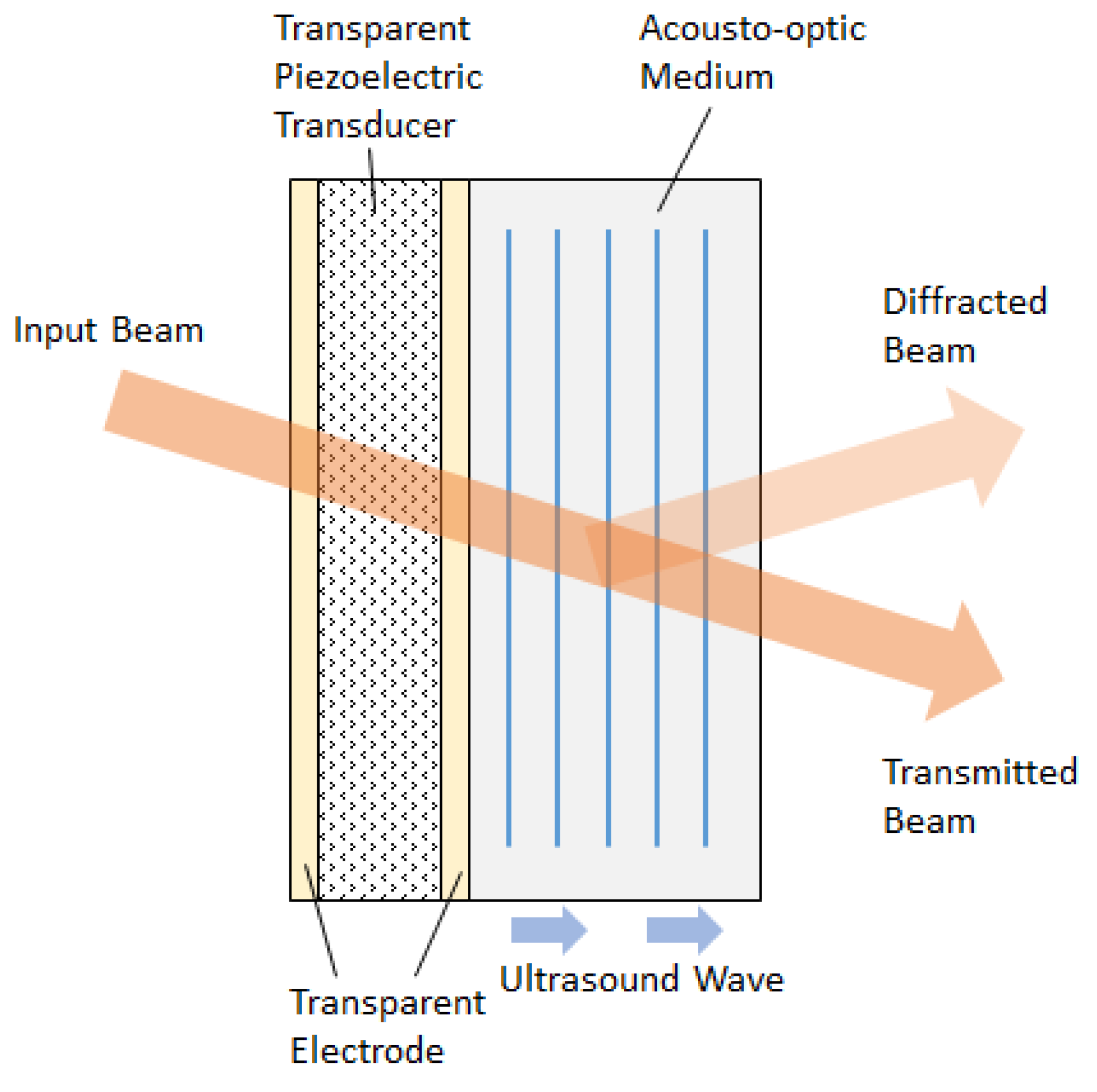
:1. Introduction
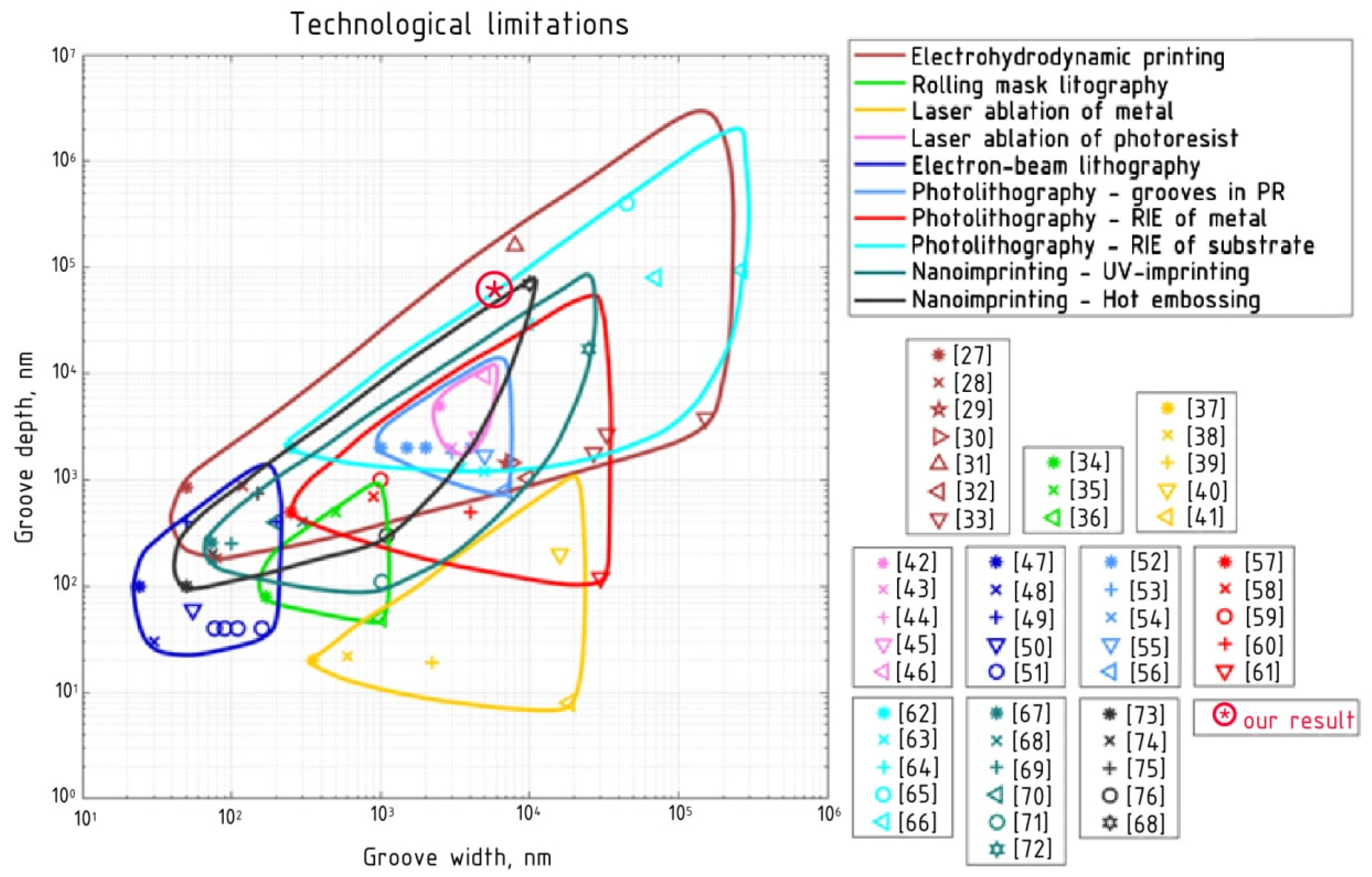
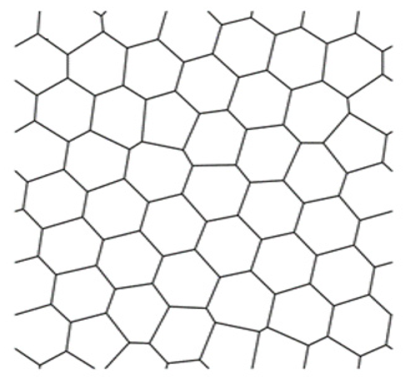
2. The Analysis of the Production Technologies of Transparent Mesh Structures
- Approaches based on the formation of grooves of a specified geometry in a substrate or photoresist and their subsequent filling with metal. The grooves are formed using photolithography methods in combination with liquid or ion plasma etching or laser ablation;
- Approaches based on the removal of the preliminarily deposited metal layer using the same etching methods;
- Approaches based on additive processes (electrohydrodynamic printing).
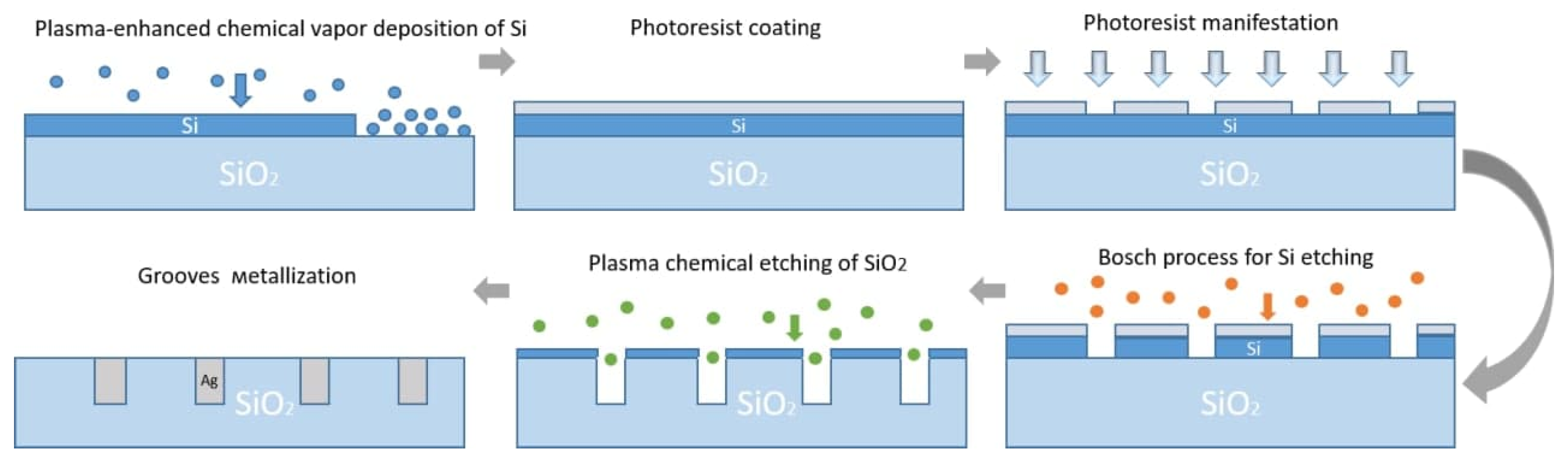
3. Materials and Methods
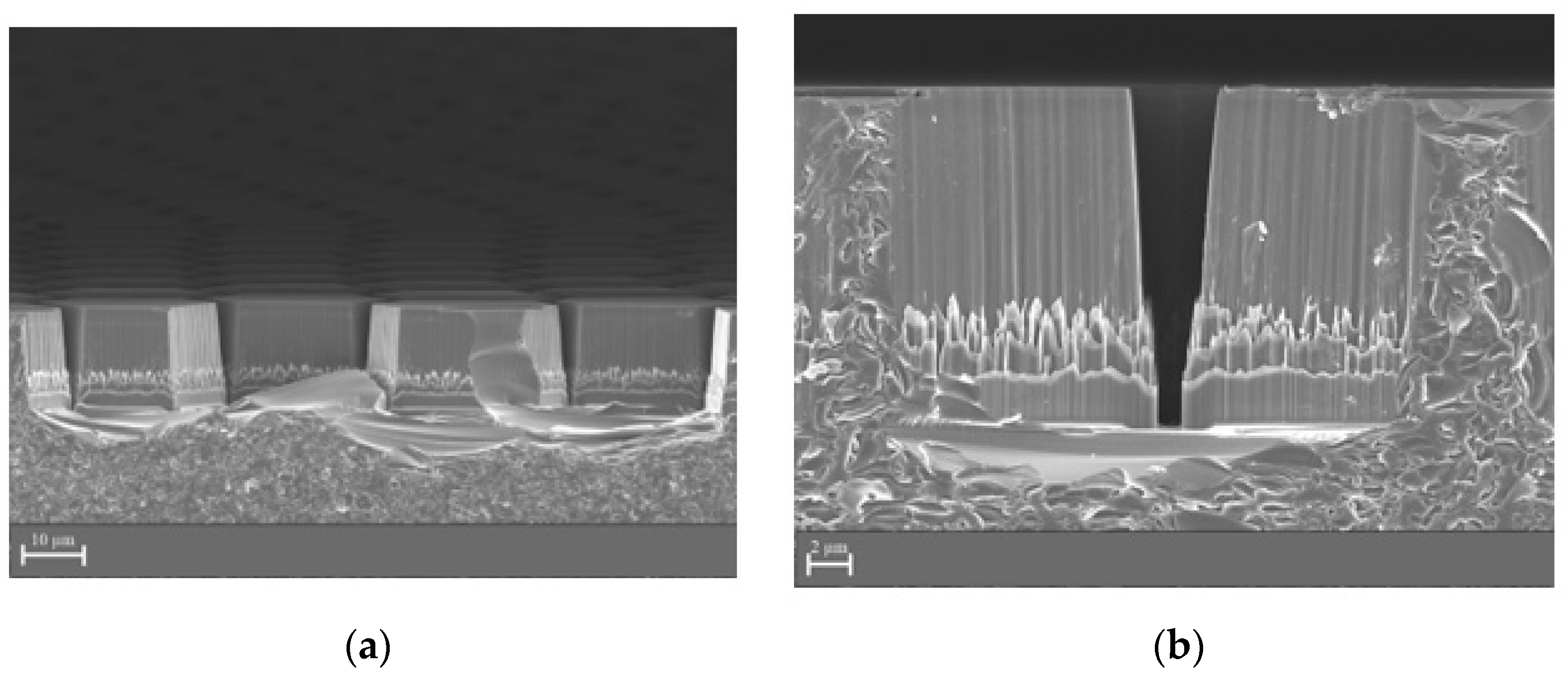
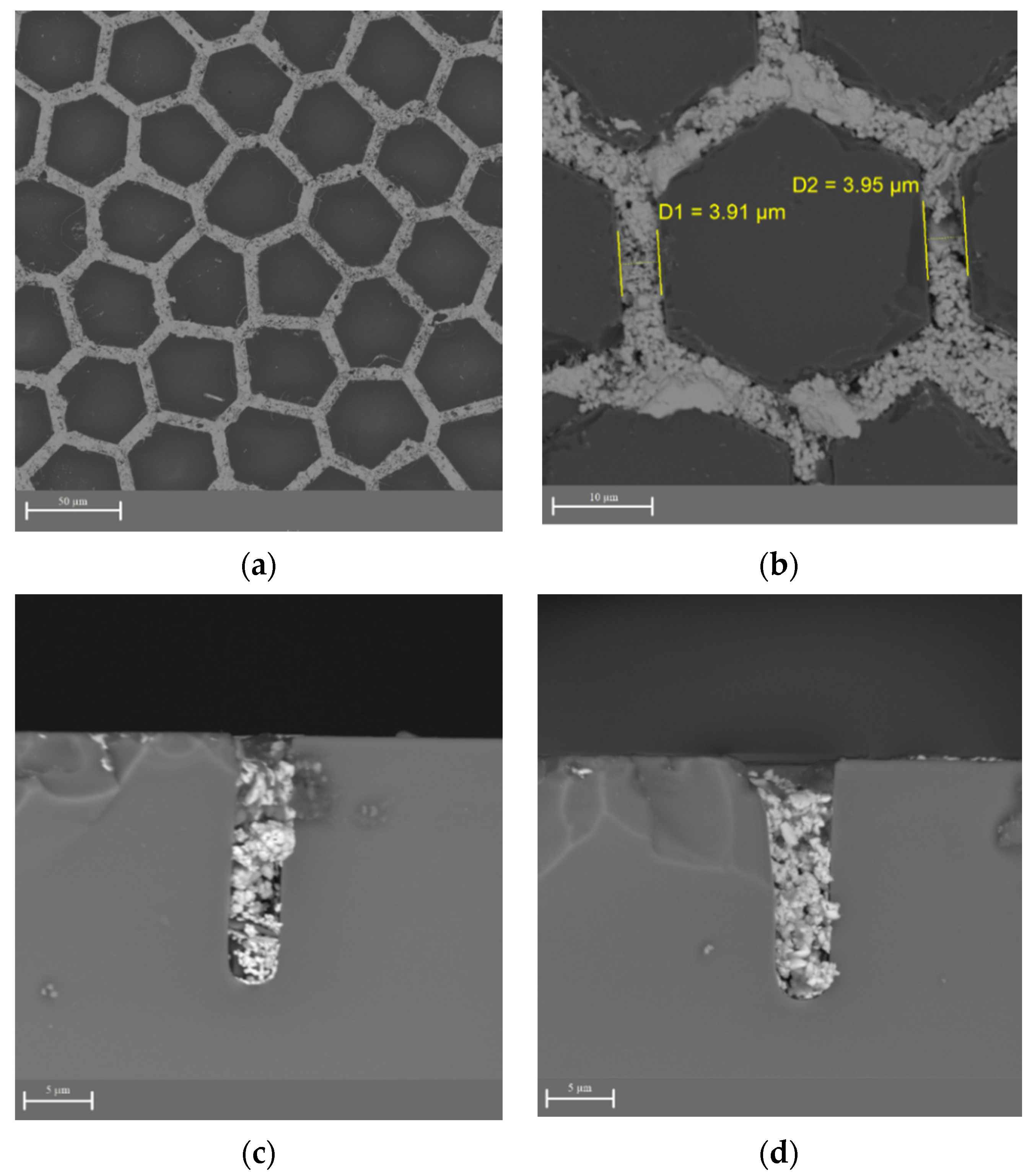
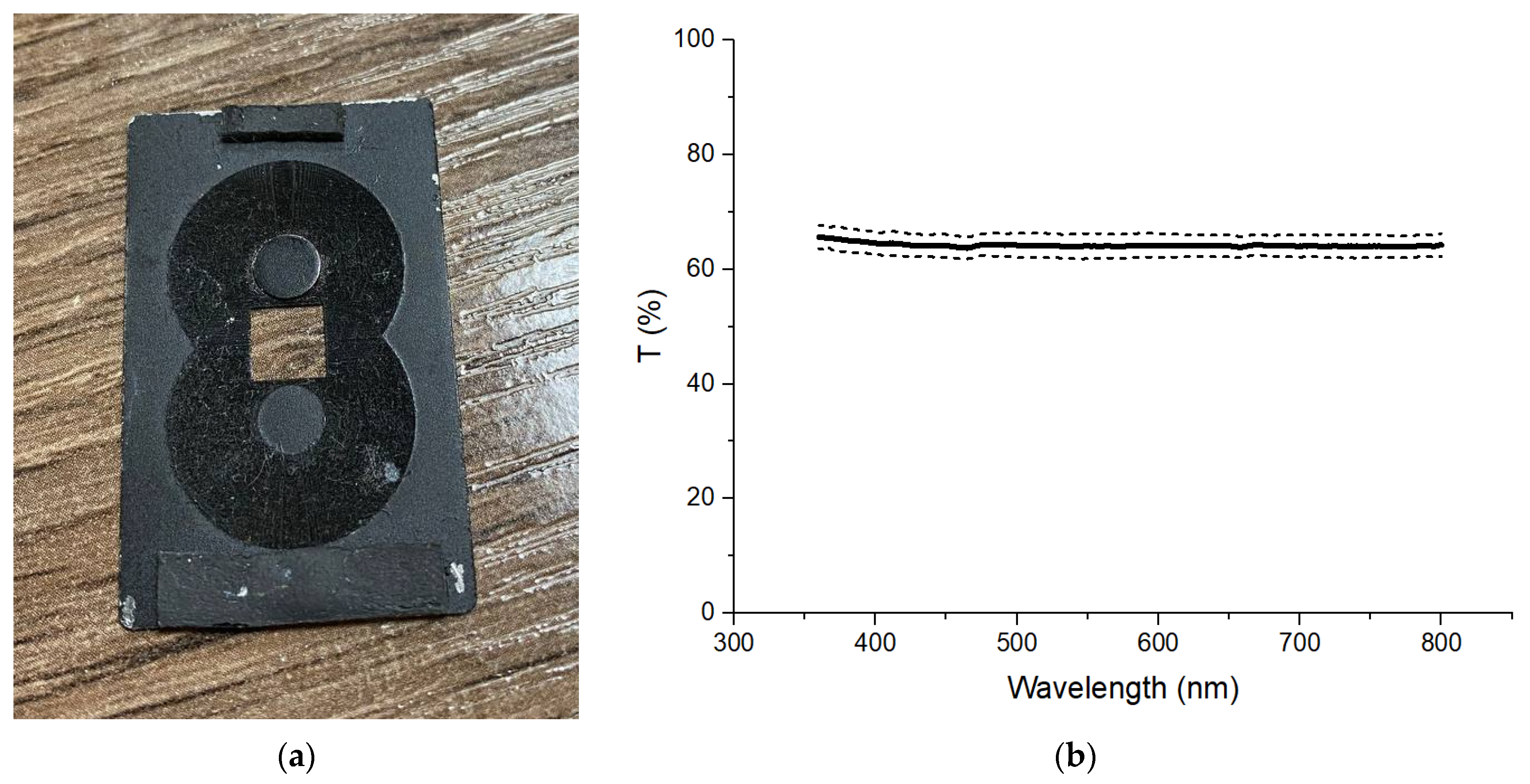
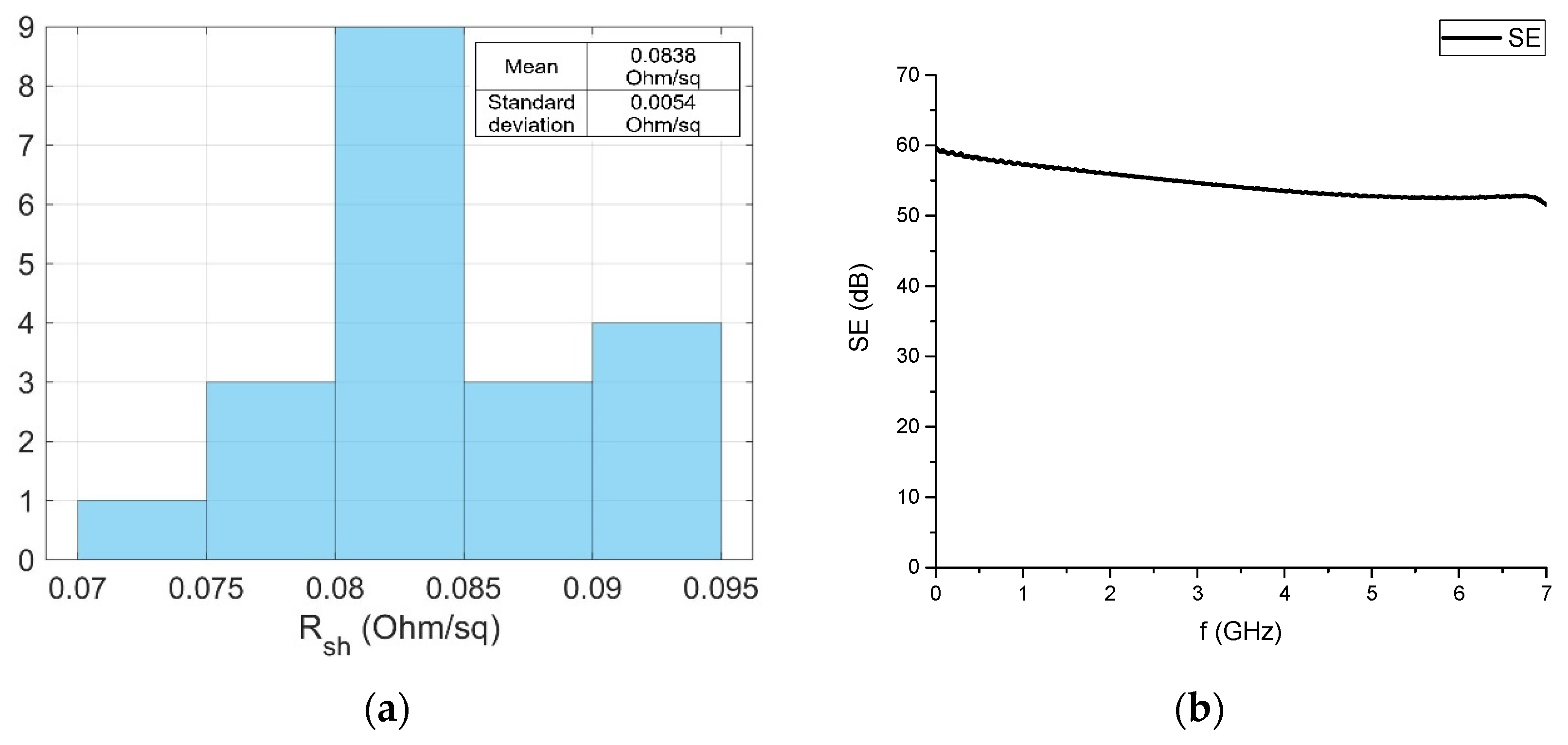
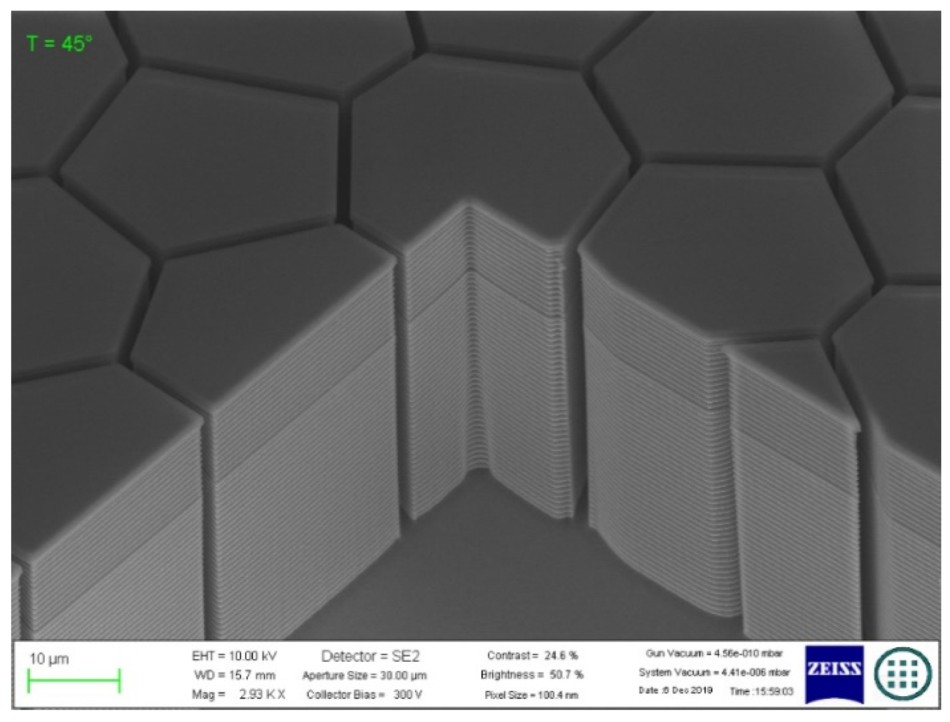
4. Results
5. Discussion
6. Conclusions
Author Contributions
Funding
Institutional Review Board Statement
Informed Consent Statement
Data Availability Statement
Acknowledgments
Conflicts of Interest
References
- Maák, P.; Lenk, S.; Jakab, L.; Barócsi, A.; Richter, P. Optimization of transducer configuration for bulk acousto-optic tunable filters. Opt. Commun. 2004, 241, 87–98. [Google Scholar] [CrossRef]
- Dühring, M.B.; Laude, V.; Khelif, A. Improving surface acousto-Optical interaction by high aspect ratio electrodes. J. Appl. Phys. 2009, 106, 113518. [Google Scholar] [CrossRef] [Green Version]
- Pannell, C.N.; Ward, J.D.; Wachman, E.S.; Zhang, B.G.; Reed, M.K. A high-Performance passband-Agile hyperspectral imager using a large aperture acousto-Optic tuneable filter. Photonic Instrum. Eng. II 2015, 9369, 936906. [Google Scholar]
- Tran, C.D.; Huang, G.C. Characterization of the collinear beam acousto-Optic tunable filter and its comparison with the noncollinear and the integrated acousto-Optic tunable filter. Opt. Eng. 1999, 38, 1143–1148. [Google Scholar] [CrossRef]
- Gupta, N.; Fell, N.F., Jr. A compact collinear AOTF Raman spectrometer. Talanta 1997, 45, 279–284. [Google Scholar] [CrossRef]
- Viskovatykh, A.; Machikhin, A.; Pozhar, V.; Pustovoit, V.I.; Viskovatykh, D.A. Combined optical-coherence and spectral microscopy based on tunable acousto-optic filters of images. Tech. Phys. Lett. 2014, 40, 157–160. [Google Scholar] [CrossRef]
- Machikhin, A.; Batshev, V.; Pozhar, V.; Naumov, A.; Gorevoy, A. Acousto-optic tunable spectral filtration of stereoscopic images. Opt. Lett. 2018, 43, 1087–1090. [Google Scholar] [CrossRef]
- Li, Z.; Ilkhechi, A.K.; Zemp, R. Transparent capacitive micromachined ultrasonic transducers (CMUTs) for photoacoustic applications. Opt. Express 2019, 27, 13204–13218. [Google Scholar] [CrossRef]
- Chen, X.; Chen, R.; Chen, Z.; Chen, J.; Shung, K.K.; Zhou, Q. Transparent lead lanthanum zirconate titanate (PLZT) ceramic fibers for high-Frequency ultrasonic transducer applications. Ceram. Int. 2016, 42, 18554–18559. [Google Scholar] [CrossRef]
- Pala, S.; Lin, L. Fully Transparent Piezoelectric Ultrasonic Transducer with 3D Printed Substrate. In Proceedings of the 20th International Conference on Solid-State Sensors, Actuators and Microsystems and Eurosensors XXXIII (Transducers and Eurosensors XXXIII), Berlin, Germany, 23–27 June 2019; pp. 234–237. [Google Scholar]
- Sette, D.; Girod, S.; Godard, N.; Adjeroud, N.; Chemin, J.B.; Leturcq, R.; Defay, E. Transparent piezoelectric transducers for large area ultrasonic actuators. In Proceedings of the IEEE 30th International Conference on Micro Electro Mechanical Systems (MEMS), Las Vegas, NV, USA, 22–26 January 2017; pp. 793–796. [Google Scholar]
- Luo, G.L.; Fung, S.; Wang, Q.; Kusano, Y.; Lasiter, J.; Kidwell, D.; Horsley, D.A. High fill factor piezoelectric micromachined ultrasonic transducers on transparent substrates. In Proceedings of the 19th International Conference on Solid-State Sensors, Actuators and Microsystems (Transducers), Kaohsiung, Taiwan, 18–22 June 2017; pp. 1053–1056. [Google Scholar]
- Ren, D.; Sun, Y.; Shi, J.; Chen, R. A Review of Transparent Sensors for Photoacoustic Imaging Applications. Photonics. Multidiscip. Digit. Publ. Inst. 2021, 8, 324. [Google Scholar] [CrossRef]
- Shehzad, M.; Wang, S.; Wang, Y. Flexible and transparent piezoelectric loudspeaker. npj Flex. Electron. 2021, 5, 1–6. [Google Scholar]
- Pasquarelli, R.M.; Ginley, D.S.; O’Hayre, R. Solution processing of transparent conductors: From flask to film. Chem. Soc. Rev. 2011, 40, 5406. [Google Scholar] [CrossRef]
- Liu, C.H.; Yu, X. Silver nanowire-Based transparent, flexible, and conductive thin film. Nanoscale Res. Lett. 2011, 6, 1. [Google Scholar] [CrossRef] [Green Version]
- Tran, N.H.; Duc, A.N.; Thanh, H.D.; Kim, H.C. Fast and simple fabrication of flexible and transparent electrode based on patterned copper nanowires by mechanical lithography transfer. Thin Solid Film. 2019, 685, 26. [Google Scholar] [CrossRef]
- López-Naranjo, E.J.; González-Ortiz, L.J.; Apátiga, L.M.; Rivera-Muñoz, E.M.; Manzano-Ramírez, A. Transparent electrodes: A review of the use of carbon-Based nanomaterials. J. Nanomater. 2016, 2016, 4928365. [Google Scholar] [CrossRef] [Green Version]
- Voronin, A.S.; Simunin, M.M.; Fadeev, Y.V.; Ivanchenko, F.S.; Karpova, D.V.; Tambasov, I.A.; Khartov, S.V. Technological basis of the formation of micromesh transparent electrodes by means of a self-Organized template and the study of their properties. Tech. Phys. Lett. 2019, 45, 366. [Google Scholar] [CrossRef]
- Lu, H.C.; Mao, J.W.; Chiang, Y.C. Low temperature preparation of ITO thin films by the coating solutions containing solvothermally synthesized ITO nanoparticles. Surf. Coat. Technol. 2013, 231, 526. [Google Scholar] [CrossRef]
- Osipkov, A.; Makeev, M.; Garsiya, E.; Filyaev, A.; Sinyagaeva, A.; Kirillov, D.; Ryzhenko, D.; Yurkov, G. Radio-Shielding metamaterials transparent in the visible spectrum: Approaches to creation. IOP Conf. Ser. Mater. Sci. Eng. IOP Publ. 2021, 1060, 012007. [Google Scholar] [CrossRef]
- Ye, S.; Rathmell, A.R.; Chen, Z.; Stewart, I.E.; Wiley, B.J. Metal nanowire networks: The next generation of transparent conductors. Adv. Mater. 2014, 26, 6670. [Google Scholar] [CrossRef]
- Levy, D.; Castellón, E. Transparent Conductive Materials: Materials. Synth. Charact. Applications, 1st ed.; Wiley-VCH: Weinheim, Germany, 2019; pp. 38–42. [Google Scholar]
- Jiang, B.; Li, M.; Bai, F.; Yu, H.; Mwenya, T.; Li, Y.; Song, D. Morphology-Controlled synthesis of silver nanoparticles on the silicon substrate by a facile silver mirror reaction. Aip Adv. 2013, 3, 032119. [Google Scholar] [CrossRef]
- Tu, Y.J.; You, C.F.; Chen, Y.R.; Huang, C.P.; Huang, Y.H. Application of recycled iron oxide for adsorptive removal of strontium. J. Taiwan Inst. Chem. Eng. 2015, 53, 92–97. [Google Scholar] [CrossRef]
- Lee, H.B.; Jin, W.Y.; Ovhal, M.M.; Kumar, N.; Kang, J.W. Flexible transparent conducting electrodes based on metal meshes for organic optoelectronic device applications: A review. J. Mater. Chem. C 2019, 7, 1087–1110. [Google Scholar] [CrossRef]
- Wolf, M.; Dretschkow, T.; Wunderle, B.; Jurgensen, N.; Engelmann, G.; Ehrmann, O.; Uhlig, A.; Michel, B.; Reichl, H. High aspect ratio TSV copper filling with different seed layers. In Proceedings of the 58th Electronic Components and Technology Conference, Lake Buena Vista, FL, USA, 27–30 May 2008; IEEE: Piscataway, NJ, USA; pp. 563–570. [Google Scholar]
- Galiker, P.; Schneider, J.; Eghlidi, H.; Kress, S.; Sandoghdar, V.; Poulikakos, D. Direct printing of nanostructures by electrostatic autofocussing of ink nanodroplets. Nat. Commun. 2012, 3, 1–9. [Google Scholar] [CrossRef]
- Schneider, J.; Rohner, P.; Thureja, D.; Schmid, M.; Galliker, P.; Poulikakos, D. Electrohydrodynamic nanodrip printing of high aspect ratio metal grid transparent electrodes. Adv. Funct. Mater. 2015, 26, 833–840. [Google Scholar] [CrossRef]
- Seong, B.; Yoo, H.; Nguyen, V.D.; Jang, Y.; Ryu, C.; Byun, D. Metal-Mesh based transparent electrode on a 3-D curved surface by electrohydrodynamic jet printing. J. Micromech. Microeng. 2014, 24, 097002. [Google Scholar] [CrossRef]
- Jang, Y.; Kim, J.; Byun, D. Invisible metal-Grid transparent electrode prepared by electrohydrodynamic (EHD) jet printing. Appl. Phys. 2013, 46, 155103. [Google Scholar] [CrossRef]
- Zhang, B.; Lee, H.; Byun, D. Electrohydrodynamic Jet Printed 3-Dimensional (3-D) Metallic Grid: Towards High-Performance Transparent Electrodes. Adv. Eng. Mater. 2020, 22, 1901275. [Google Scholar] [CrossRef]
- Sujaya, K.; Do-Geun, K.; Jihoon, K. Electromagnetic interference shielding effectiveness of invisible metal-Mesh prepared by electrohydrodynamic jet printing. Jpn. Soc. Appl. Phys. 2014, 53, 05HB11. [Google Scholar]
- Jang, Y.; Hartarto Tambunan, I.; Tak, H.; Dat Nguyen, V.; Kang, T.; Byun, D. Non-Contact printing of high aspect ratio Ag electrodes for polycrystalline silicone solar cell with electrohydrodynamic jet printing. Appl. Phys. Lett. 2013, 102, 123901. [Google Scholar] [CrossRef]
- Kwak, M.K.; Ok, J.G.; Lee, J.Y.; Guo, L.J. Continuous phase-Shift lithography with a roll-Type mask and application to transparent conductor fabrication. Nanotechnology 2012, 23, 344008. [Google Scholar] [CrossRef] [Green Version]
- Chen, J.; Cranton, W.; Fihn, M. Handbook of Visual Display Technology; Springer: Berlin/Heidelberg, Germany, 2016. [Google Scholar]
- Ok, J.G.; Kwak, M.K.; Huard, C.M.; Youn, H.S.; Guo, L.J. Photo-Roll Lithography (PRL) for Continuous and Scalable Patterning with Application in Flexible Electronics. Adv. Mater. 2013, 25, 6554–6561. [Google Scholar] [CrossRef] [PubMed] [Green Version]
- Eckhardt, S.; Müller-Meskamp, L.; Loeser, M.; Siebold, M.; Lasagni, A.F. Fabrication of highly efficient transparent metal thin film electrodes using Direct Laser Interference Patterning. Laser-Based Micro-Nanoprocessing IX 2015, 9351, 935116. [Google Scholar]
- Müller-Meskamp, L.; Schubert, S.; Roch, T.; Eckhardt, S.; Lasagni, A.F.; Leo, K. Transparent Conductive Metal Thin-Film Electrodes Structured by Direct Laser Interference Patterning. Adv. Eng. Mater. 2015, 17, 1400454. [Google Scholar] [CrossRef]
- Paeng, D.; Yoo, J.H.; Yeo, J.; Lee, D.; Kim, E.; Ko, S.H.; Grigoropoulos, C.P. Low-Cost Facile Fabrication of Flexible Transparent Copper Electrodes by Nanosecond Laser Ablation. Adv. Mater. 2015, 27, 1500098. [Google Scholar] [CrossRef] [PubMed]
- Qin, R.; Hu, M.; Zhang, N.; Guo, Z.; Yan, Z.; Li, J.; Liu, J.; Shan, G.; Yang, J. Flexible Fabrication of Flexible Electronics: A General Laser Ablation Strategy for Robust Large-Area Copper-Based Electronics. Adv. Electron. Mater. 2019, 5, 1900365. [Google Scholar] [CrossRef]
- Wang, Q.; Li, B.J.; Toor, F.; Ding, H. Novel laser-Based metasurface fabrication process for transparent conducting surfaces. J. Laser Appl. 2019, 31, 022505. [Google Scholar] [CrossRef]
- Liu, Y.H.; Xu, J.L.; Gao, X.; Sun, Y.L.; Lv, J.J.; Shen, S.; Chen, L.S.; Wang, S.D. Freestanding transparent metallic network based ultrathin, foldable and designable supercapacitors. Energy Environ. Sci. 2017, 10, 2534–2543. [Google Scholar] [CrossRef]
- Li, M.; Zuo, W.W.; Ricciardulli, A.G.; Yang, Y.G.; Liu, Y.H.; Wang, Q.; Wang, K.L.; Li, G.X.; Saliba, M.; Girolamo, D.D.; et al. Embedded Nickel-Mesh Transparent Electrodes for Highly Efficient and Mechanically Stable Flexible Perovskite Photovoltaics: Toward a Portable Mobile Energy Source. Adv. Mater. 2020, 32, 2003422. [Google Scholar] [CrossRef]
- Xu, J.L.; Liu, Y.H.; Gao, X.; Sun, Y.; Shen, S.; Cai, X.; Chen, L.; Wang, S.D. Embedded Ag Grid Electrodes as Current Collector for Ultra-Flexible Transparent Solid-State Supercapacitor. ACS Appl. Mater. Interfaces 2017, 9, 27649. [Google Scholar] [CrossRef]
- Liu, Y.H.; Xu, J.L.; Shen, S.; Cai, X.L.; Chen, L.S.; Wang, S.D. High-performance, ultra-flexible and transparent embedded metallic mesh electrodes by selective electrodeposition for all-solid-state supercapacitor applications. J. Mater. Chem. A 2017, 5, 9032–9041. [Google Scholar] [CrossRef]
- Jiang, Z.Y.; Huang, W.; Chen, L.S.; Liu, Y.H. Ultrathin, lightweight, and freestanding metallic mesh for transparent electromagnetic interference shielding. Opt. Express 2019, 27, 24194–24206. [Google Scholar] [CrossRef]
- Bilenberg, B.; Jacobsen, S.; Schmidt, M.S.; Skjolding, L.H.D.; Shi, P.; Bøggild, P.; Tegenfeldt, J.O.; Kristensena, A. High resolution 100 kV electron beam lithography in SU-8. Microelectron. Eng. 2006, 83, 1609–1612. [Google Scholar] [CrossRef]
- Taylor, A.B.; Michaux, P.; Mohsin, A.S.; Chon, J.W. Electron-beam lithography of plasmonic nanorod arrays for multilayered optical storage. Opt. Express 2014, 22, 13234–13243. [Google Scholar] [CrossRef] [PubMed]
- Rai-Choudhury, P. Handbook of Microlithography, Micromachining, and Microfabrication: Micromachining and Microfabrication; SPIE Press: Washington, DC, USA, 1997; Volume 2, pp. 41–99. [Google Scholar]
- Groep, J.; Spinelli, P.; Polman, A. Transparent Conducting Silver Nanowire Networks. Nano Lett. 2012, 12, 3138–3144. [Google Scholar] [CrossRef]
- Wang, L.; Xiong, W.; Nishijima, Y.; Yokota, Y.; Ueno, K.; Misawa, H.; Qiu, J.; Bi, G. Spectral properties of nanoengineered Ag/Au bilayer rods fabricated by electron beam lithography. Appl. Opt. 2011, 50, 5600–5605. [Google Scholar] [CrossRef] [PubMed]
- DONGJIN Photoresist Products DSAM-3000 Series. Available online: https://www.yumpu.com/en/document/read/29811371/dongjin-photoresist-products-dsam-3000-series (accessed on 31 October 2021).
- Zhang, C.; Khan, A.; Cai, J.; Liang, C.; Liu, Y.; Deng, J.; Huang, S.; Li, G.; Li, W.D. Stretchable Transparent Electrodes with Solution-processed Regular Metal Mesh for Electroluminescent Light-emitting Film. ACS Appl. Mater. Interfaces 2018, 10, 21009–21017. [Google Scholar] [CrossRef]
- Khan, A.; Lee, S.; Jang, T.; Xiong, Z.; Zhang, C.; Tang, J.; Guo, L.J.; Li, W.D. High-Performance Flexible Transparent Electrode with an Embedded Metal Mesh Fabricated by Cost-Effective Solution Process. Small 2016, 12, 3021–3030. [Google Scholar] [CrossRef]
- Wang, W.; Bai, B.; Zhou, Q.; Ni, K.; Lin, H. Petal-shaped metallic mesh with high electromagnetic shielding efficiency and smoothed uniform diffraction. Opt. Mater. Express 2018, 8, 3485–3493. [Google Scholar] [CrossRef]
- Zhao, L.; Yu, S.; Li, X.; Wu, M.; Li, L. High-Performance copper mesh transparent flexible conductors based on electroplating with vacuum-Free processing. Org. Electron. 2019, 82, 105511. [Google Scholar] [CrossRef]
- Xie, R.; Kava, J.; Siegel, M. Aspect ratio dependent etching on metal etch: Modeling and experiment. J. Vac. Sci. Technol. A Vac. Surf. Film. 1996, 14, 1067–1071. [Google Scholar] [CrossRef]
- Blumenstock, K.; Stephani, D. Anisotropic reactive ion etching of titanium. J. Vac. Sci. Technol. B 1989, 7, 627. [Google Scholar] [CrossRef]
- Hu, C.; Small, M.; Schadt, M. Reactive Ion Etching of AI(Cu) Alloys. MRS Online Proceeding Libr. Arch. 1986, 76, 191–195. [Google Scholar] [CrossRef]
- Howard, B.J.; Wolterman, S.K.; Yoo, W.J.; Gittleman, B.; SteinbrÜchel, C.H. Reactive Ion Etching of Copper with SiCl4 and CCl2F2. MRS Online Proceeding Libr. Arch. 2011, 201, 129–133. [Google Scholar] [CrossRef]
- Jin, S.W.; Lee, Y.H.; Yeom, K.M.; Yun, J.; Park, H.; Jeong, Y.R.; Hong, S.Y.; Lee, G.; Oh, S.Y.; Lee, J.H.; et al. Highly Durable and Flexible Transparent Electrode for Flexible Optoelectronic Applications. ACS Appl. Mater. Interfaces 2018, 10, 30706–30715. [Google Scholar] [CrossRef]
- Leech, P.; Reeves, G. Reactive ion etching of quartz and glasses for microfabrication. Proc. SPIE 1999, 3680, 341281. [Google Scholar]
- Holland, A.; Leech, P.; Reeves, G. Reactive ion etching of organic polymers for application in waveguide trench molds. J. Mater. Sci. 2004, 39, 3505–3508. [Google Scholar] [CrossRef]
- Queste, S.; Courjon, E.; Ulliac, G.; Salut, R.; Petrini, V.; Rauch, J.; Besançon Cedex, F. Deep Reactive Ion Etching of quartz, lithium niobate and lead titanate. JNTE Proc. 2008, 1, 1–2. [Google Scholar]
- Zhang, C.; Yang, C.; Ding, D. Deep reactive ion etching of PMMA. Appl. Surf. Sci. 2004, 227, 139. [Google Scholar] [CrossRef]
- Chapellier, P.; Lavenus, P.; Bourgeteau-Verlhac, B.; Gageant, C.; Le Traon, O.; Dulmet, B. Aspect ratio dependent etching in advanced deep reactive ion etching of quartz. In Proceedings of the 2017 Symposium on Design, Test, Integration and Packaging of MEMS/MOEMS (DTIP), Bordeaux, France, 29 May–1 June 2017; pp. 1–6. [Google Scholar]
- Zhong, Y.; Yuen, M. Hard mold UV nanoimprint lithography process. In Proceedings of the 2012 14th International Conference on Electronic Materials and Packaging (EMAP), Hong Kong, China, 13–16 December 2012; pp. 1–5. [Google Scholar]
- Nanoimprint Lithography (NIL)-SmartNIL®. Available online: https://www.evgroup.com/technologies/nanoimprint-lithography-smartnil/ (accessed on 26 May 2021).
- Fukuhara, M.; Ono, H.; Hirasawa, T.; Otaguchi, M.; Sakai, N.; Mizuno, J.; Shoji, S. UV Nanoimprint Lithography and Its Application for Nanodevices. J. Photopolym. Sci. Technol. 2007, 20, 549–554. [Google Scholar] [CrossRef]
- Hashmi, S. Reference Module in Materials Science and Materials Engineering; Elsevier: Oxford, UK, 2016; pp. 1–8. [Google Scholar]
- Kawaguchi, Y.; Nonaka, F.; Sanada, Y. Fluorinated materials for UV nanoimprint lithography. Microelectron. Eng. 2007, 84, 973–976. [Google Scholar] [CrossRef]
- Jianyun, H.; Changsong, Z.; Fan, Y.; Jinghui, Z.; Jinge, T.; Weimin, Y. UV-Curable micro-imprinting method for the fabrication of microstructure arrays. Microsyst. Technol. 2019, 25, 3311–3316. [Google Scholar] [CrossRef]
- Wang, M. Lithography; IntechOpen: London, UK, 2010; pp. 457–494. [Google Scholar]
- Tang, A.; He, S.; Lee, M. Fabrication of III–V compound nanowires via hot embossing nanoimprint lithography. Jpn. J. Appl. Phys. 2016, 55, 035001. [Google Scholar] [CrossRef]
- Chen, Y. Applications of nanoimprint lithography/hot embossing: A review. Appl. Phys. A 2015, 121, 451–465. [Google Scholar] [CrossRef]
- Roos, N.; Luxbacher, T.; Glinsner, T.; Pfeiffer, K.; Schulz, H.; Scheer, H.C. Nanoimprint lithography with a commercial 4-in. bond system for hot embossing. Proc. SPIE 2001, 4343, 427–435. [Google Scholar]
- Shiriaev, P.P.; Ryzhenko, D.S.; Makeev, M.O. Simulation of transparent electromagnetic interference shielding materials based on periodic conductive networks. J. Phys. Conf. Series. IOP Publ. 2019, 1410, 012206. [Google Scholar] [CrossRef]
- Shiriaev, P.; Makeev, M.; Ryzhenko, D.; Popkov, O. Theoretical study of electromagnetic and optical properties of periodic conductive networks based on Voronoi diagrams. Mater. Today Proc. 2019, 19, 2179–2182. [Google Scholar] [CrossRef]
- Vansovskaya, K.M. Metal coatings applied by chemical method. Mashinostroenie 1985, 2, 81–85. [Google Scholar]
- Shalkauskas, M.I.; Vashkialis, A.I. Chemical Metallization of Plastics, 3rd ed.; Chimia: Saint-Petersburg, Russia, 1985; pp. 137–142. [Google Scholar]
- Shi, Y.; Li, Y.; Zhang, J.; Yu, Z.; Yang, D. Electrospun polyacrylonitrile nanofibers loaded with silver nanoparticles by silver mirror reaction. Mater. Sci. Eng. C 2015, 51, 346–355. [Google Scholar] [CrossRef]


Publisher’s Note: MDPI stays neutral with regard to jurisdictional claims in published maps and institutional affiliations. |
© 2021 by the authors. Licensee MDPI, Basel, Switzerland. This article is an open access article distributed under the terms and conditions of the Creative Commons Attribution (CC BY) license (https://creativecommons.org/licenses/by/4.0/).
Share and Cite
Osipkov, A.; Makeev, M.; Konopleva, E.; Kudrina, N.; Gorobinskiy, L.; Mikhalev, P.; Ryzhenko, D.; Yurkov, G. Optically Transparent and Highly Conductive Electrodes for Acousto-Optical Devices. Materials 2021, 14, 7178. https://doi.org/10.3390/ma14237178
Osipkov A, Makeev M, Konopleva E, Kudrina N, Gorobinskiy L, Mikhalev P, Ryzhenko D, Yurkov G. Optically Transparent and Highly Conductive Electrodes for Acousto-Optical Devices. Materials. 2021; 14(23):7178. https://doi.org/10.3390/ma14237178
Chicago/Turabian StyleOsipkov, Alexey, Mstislav Makeev, Elizaveta Konopleva, Natalia Kudrina, Leonid Gorobinskiy, Pavel Mikhalev, Dmitriy Ryzhenko, and Gleb Yurkov. 2021. "Optically Transparent and Highly Conductive Electrodes for Acousto-Optical Devices" Materials 14, no. 23: 7178. https://doi.org/10.3390/ma14237178
APA StyleOsipkov, A., Makeev, M., Konopleva, E., Kudrina, N., Gorobinskiy, L., Mikhalev, P., Ryzhenko, D., & Yurkov, G. (2021). Optically Transparent and Highly Conductive Electrodes for Acousto-Optical Devices. Materials, 14(23), 7178. https://doi.org/10.3390/ma14237178