
Progress in Perovskite Solar Cells towards Commercialization—A Review


 and
and 
Abstract
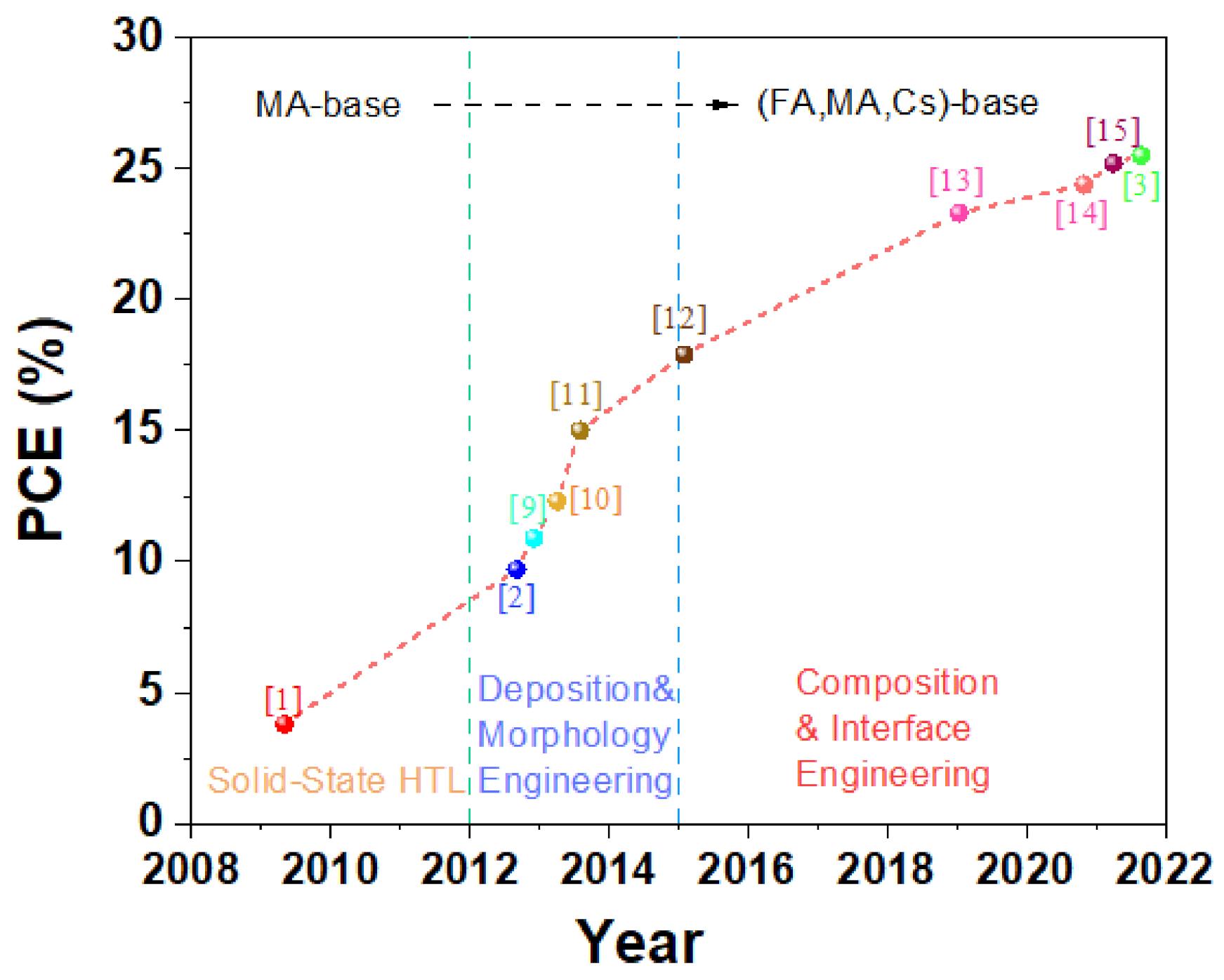
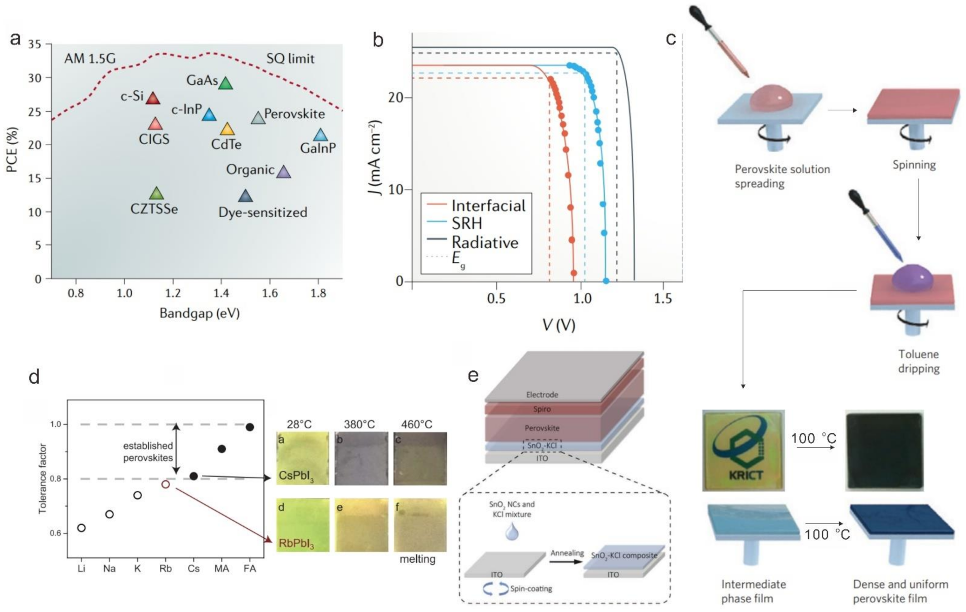
:1. Introduction
2. Improved Performance of Large-Area PSMs

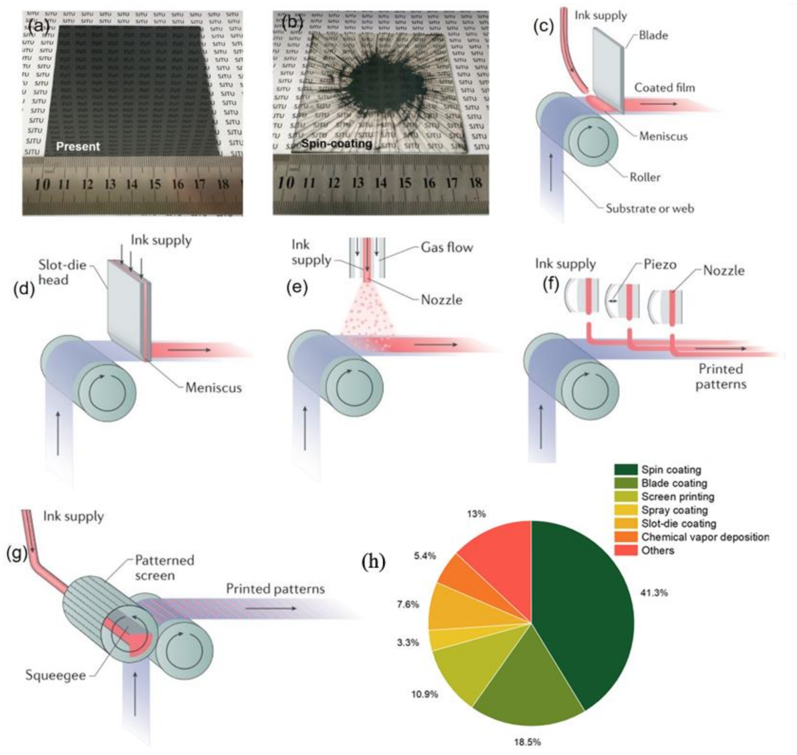
2.1. Scalable Coating Methods
2.1.1. Blade Coating
2.1.2. Slot-Die Coating
2.1.3. Spray Coating
2.1.4. Inkjet Printing
2.1.5. Screen Printing

2.2. Upscaling of the Absorber Layer
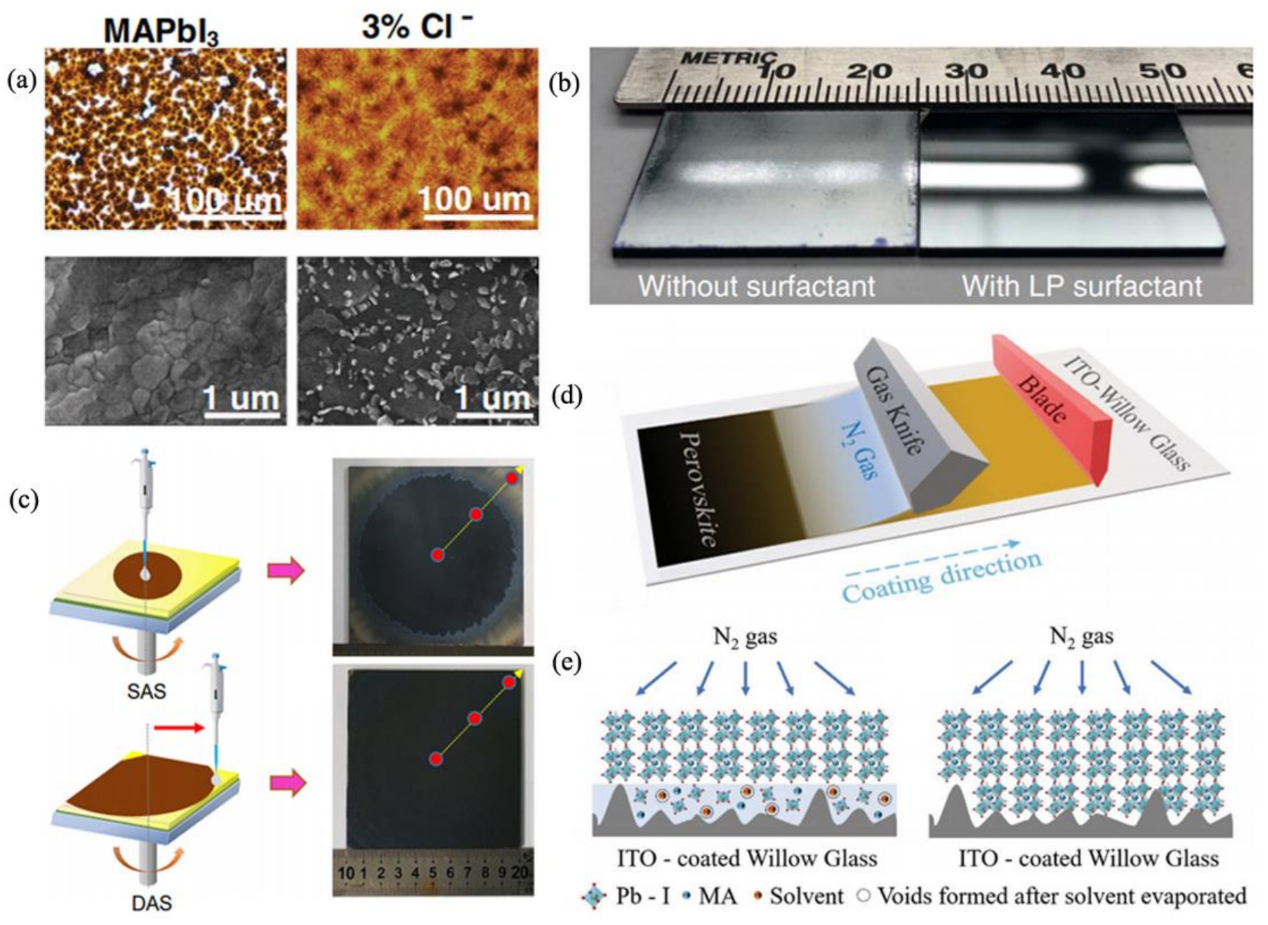
2.2.1. Compositional Engineering
2.2.2. Solvent and Antisolvent Engineering
2.2.3. Physical Methods

2.3. Upscaling of the Transport Layer (ETL & HTL) and Back Electrode
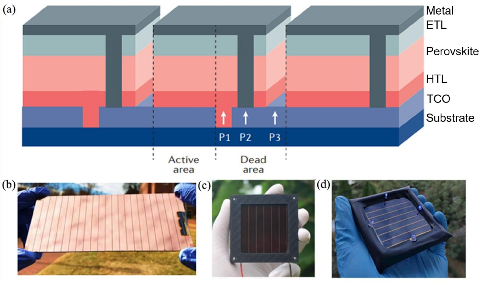
2.4. Module Design
2.4.1. Fabrication of Series Connected Modules
2.4.2. Optimization of Series-Connected Modules
3. Stability of PSCs
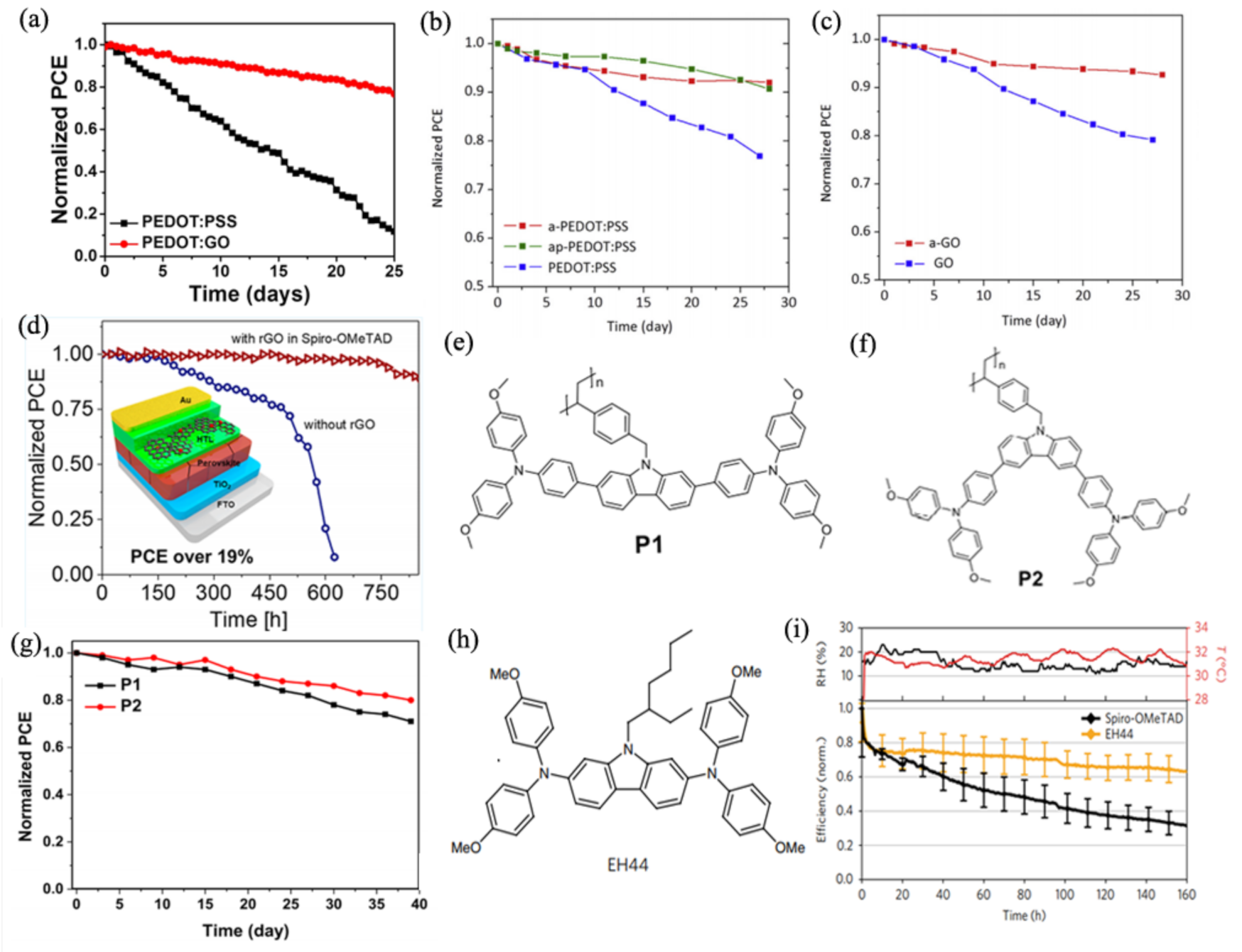
3.1. The Stability of the Hole Transport Layer
3.1.1. Organic HTMs

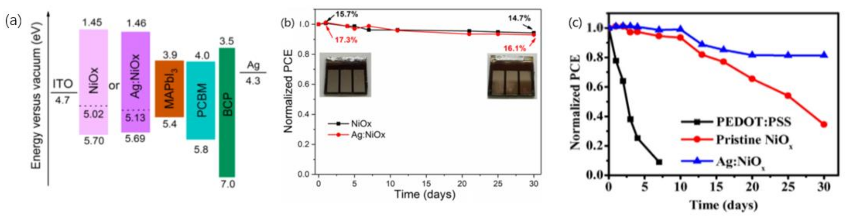
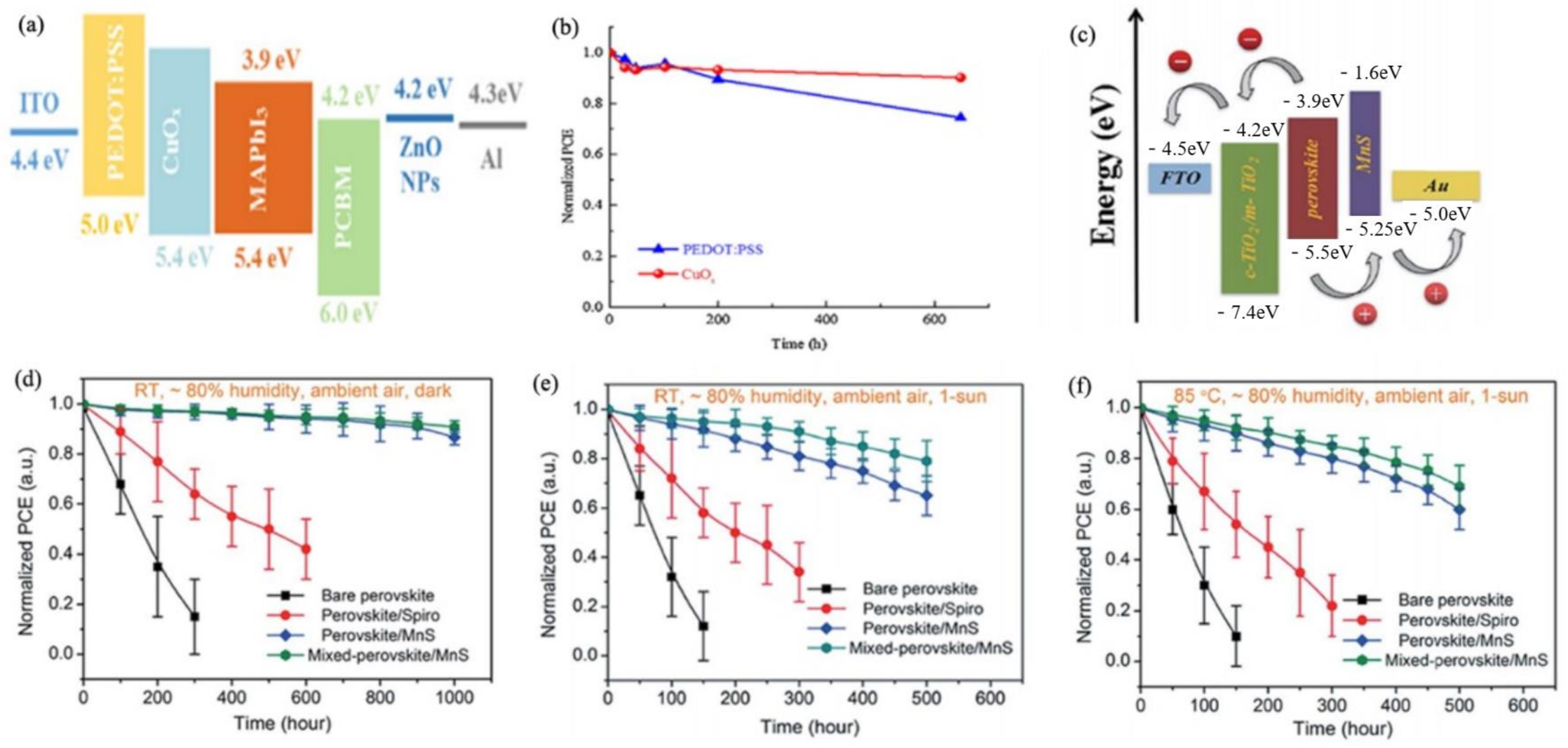
3.1.2. Inorganic HTMs

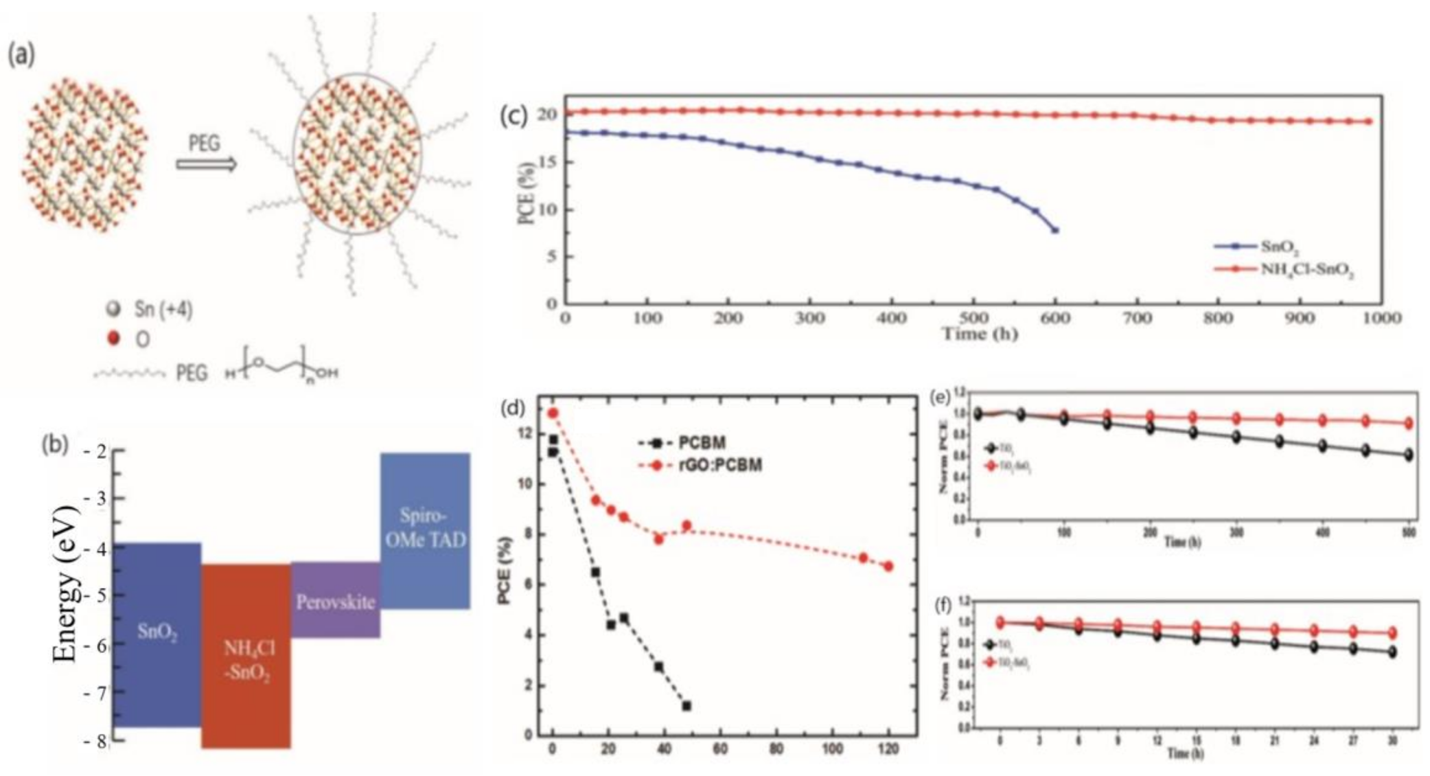
3.2. The Stability of the Electron Transport Layer

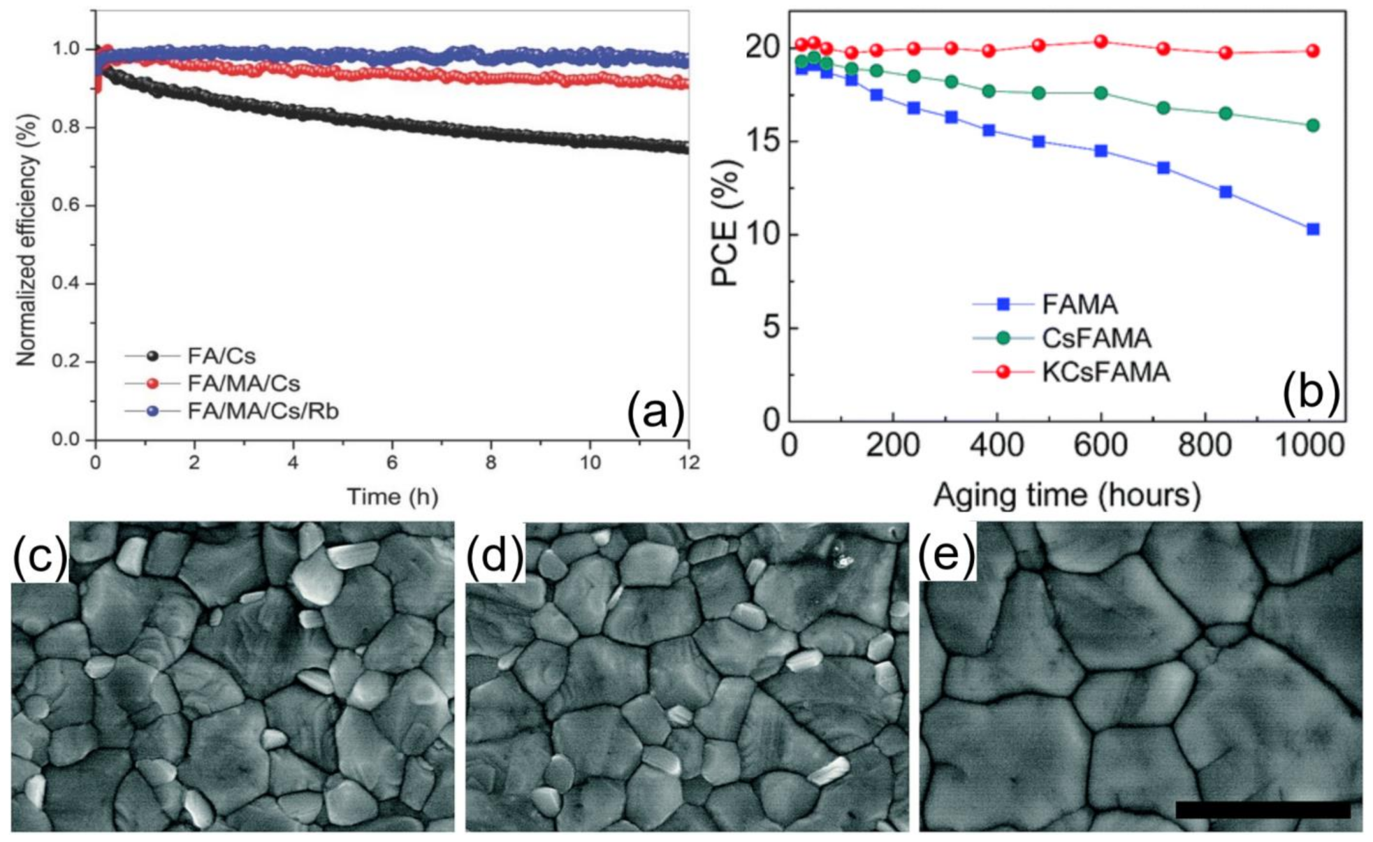
3.3. The Stability of the Perovskite Layer
3.3.1. Organic–Inorganic Hybrid Perovskites


3.3.2. All-Inorganic PSCs
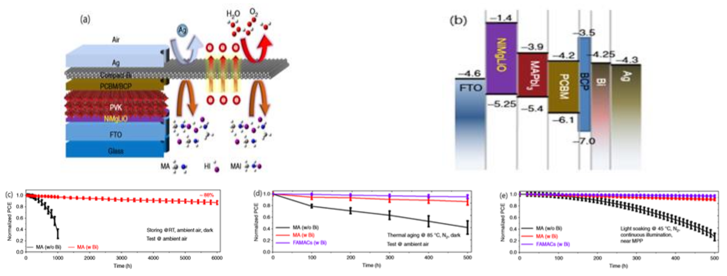
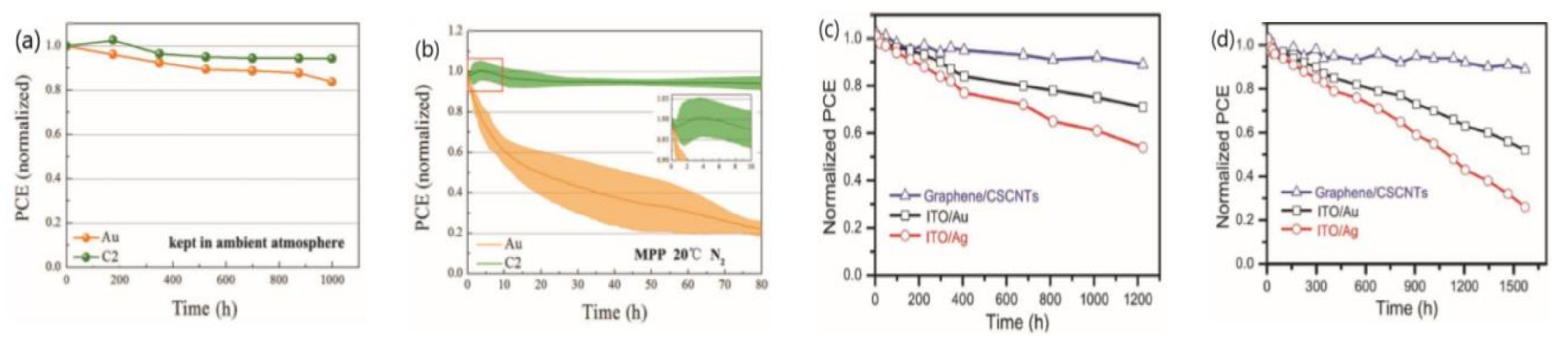
3.4. The Stability of Electrodes
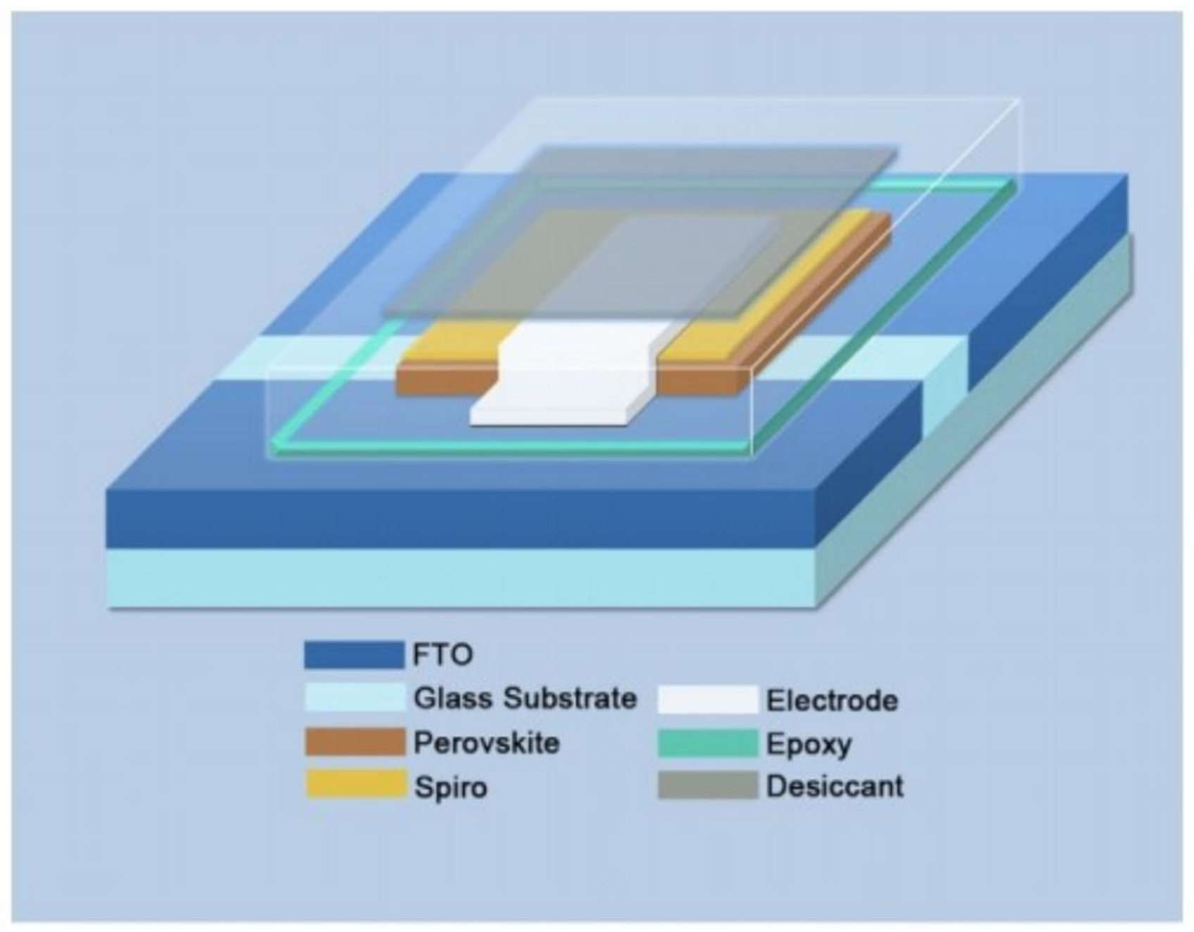
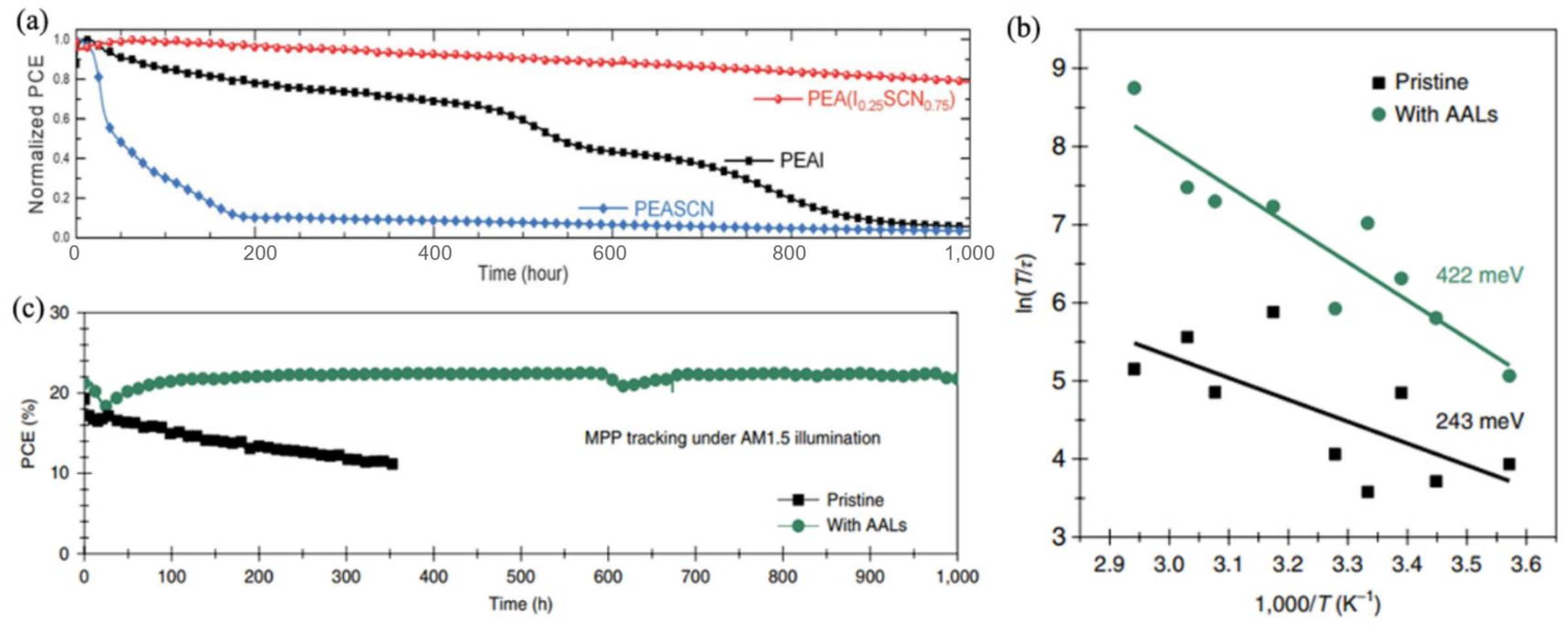
3.5. External Encapsulation Engineering
4. Other Issues of Commercialization
4.1. Risk and Hazards
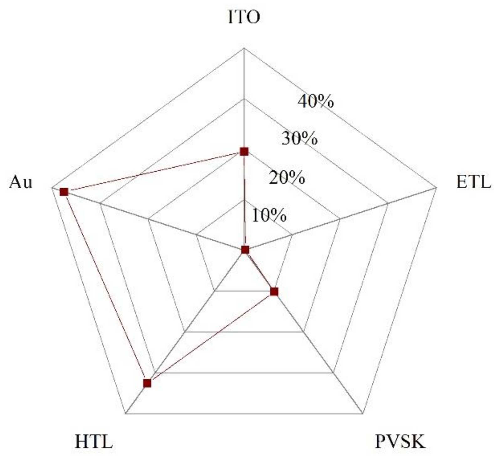
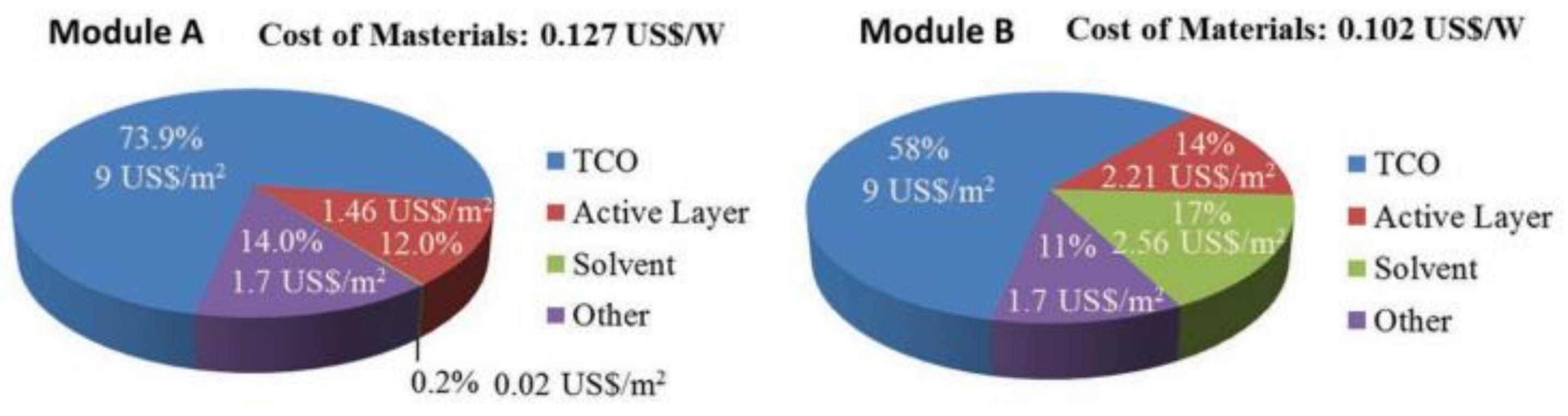
4.2. Cost-Related Analysis


5. Conclusions and Perspectives
Supplementary Materials
Author Contributions
Funding
Institutional Review Board Statement
Informed Consent Statement
Data Availability Statement
Conflicts of Interest
References
- Kojima, A.; Teshima, K.; Shirai, Y.; Miyasaka, T. Organometal Halide Perovskites as Visible-light Sensitizers for Photovoltaic Cells. J. Am. Chem. Soc. 2009, 131, 6050–6051. [Google Scholar] [CrossRef] [PubMed]
- Kim, H.-S.; Lee, C.-R.; Im, J.-H.; Lee, K.-B.; Moehl, T.; Marchioro, A.; Moon, S.-J.; Humphry-Baker, R.; Yum, J.-H.; Moser, J.E. Lead iodide perovskite sensitized all-solid-state submicron thin film mesoscopic solar cell with efficiency exceeding 9%. Sci. Rep. 2012, 2, 1–7. [Google Scholar] [CrossRef] [PubMed] [Green Version]
- Best Research-Cell Efficiencies, NREL. Available online: https://www.nrel.gov/pv/assets/pdfs/best-research-cell-efficiencies-rev210726.pdf (accessed on 31 July 2021).
- Hao, F.; Stoumpos, C.C.; Cao, D.H.; Chang, R.P.H.; Kanatzidis, M.G. Lead-free solid-state organic–inorganic halide perovskite solar cells. Nat. Photonics 2014, 8, 489–494. [Google Scholar] [CrossRef]
- Pellet, N.; Gao, P.; Gregori, G.; Yang, T.Y.; Nazeeruddin, M.K.; Maier, J.; Gratzel, M. Mixed-organic-cation perovskite photovoltaics for enhanced solar-light harvesting. Angew. Chem. Int. Ed. 2014, 53, 3151–3157. [Google Scholar] [CrossRef]
- Lin, Q.; Armin, A.; Nagiri, R.C.R.; Burn, P.L.; Meredith, P. Electro-optics of perovskite solar cells. Nat. Photonics 2014, 9, 106–112. [Google Scholar] [CrossRef]
- Stranks, S.D.; Eperon, G.E.; Grancini, G.; Menelaou, C.; Alcocer, M.J.; Leijtens, T.; Herz, L.M.; Petrozza, A.; Snaith, H.J. Electron-hole diffusion lengths exceeding 1 micrometer in an organometal trihalide perovskite absorber. Science 2013, 342, 341–344. [Google Scholar] [CrossRef] [Green Version]
- Jones, T.W.; Osherov, A.; Alsari, M.; Sponseller, M.; Duck, B.C.; Jung, Y.-K.; Settens, C.; Niroui, F.; Brenes, R.; Stan, C.V.; et al. Lattice strain causes non-radiative losses in halide perovskites. Energy Environ. Sci. 2019, 12, 596–606. [Google Scholar] [CrossRef] [Green Version]
- Lee, M.M.; Teuscher, J.; Miyasaka, T.; Murakami, T.N.; Snaith, H.J. Efficient hybrid solar cells based on meso-superstructured organometal halide perovskites. Science 2012, 338, 643–647. [Google Scholar] [CrossRef] [Green Version]
- Ball, J.M.; Lee, M.M.; Hey, A.; Snaith, H.J. Low-temperature processed meso-superstructured to thin-film perovskite solar cells. Energy Environ. Sci. 2013, 6, 1739–1743. [Google Scholar] [CrossRef]
- Burschka, J.; Pellet, N.; Moon, S.J.; Humphry-Baker, R.; Gao, P.; Nazeeruddin, M.K.; Gratzel, M. Sequential deposition as a route to high-performance perovskite-sensitized solar cells. Nature 2013, 499, 316–319. [Google Scholar] [CrossRef]
- Jeon, N.J.; Noh, J.H.; Yang, W.S.; Kim, Y.C.; Ryu, S.; Seo, J.; Seok, S.I. Compositional engineering of perovskite materials for high-performance solar cells. Nature 2015, 517, 476–480. [Google Scholar] [CrossRef]
- Jiang, Q.; Zhao, Y.; Zhang, X.; Yang, X.; Chen, Y.; Chu, Z.; Ye, Q.; Li, X.; Yin, Z.; You, J. Surface Passivation of Perovskite Film for Efficient Solar Cells. Nat. Photonics 2019, 13, 460–466. [Google Scholar] [CrossRef]
- Kim, G.; Min, H.; Lee, K.S.; Lee, D.Y.; Yoon, S.M.; Seok, S.I. Impact of strain relaxation on performance of alpha-formamidinium lead iodide perovskite solar cells. Science 2020, 370, 108–112. [Google Scholar] [CrossRef]
- Jeong, J.; Kim, M.; Seo, J.; Lu, H.; Ahlawat, P.; Mishra, A.; Yang, Y.; Hope, M.A.; Eickemeyer, F.T.; Kim, M.; et al. Pseudo-halide anion engineering for alpha-FAPbI3 perovskite solar cells. Nature 2021, 592, 381–385. [Google Scholar] [CrossRef]
- Deng, Y.; Xu, S.; Chen, S.; Xiao, X.; Zhao, J.; Huang, J. Defect compensation in formamidinium-caesium perovskites for highly efficient solar mini-modules with improved photostability. Nat. Energy 2021, 6, 633–641. [Google Scholar] [CrossRef]
- Hashmi, S.G.; Tiihonen, A.; Martineau, D.; Ozkan, M.; Vivo, P.; Kaunisto, K.; Ulla, V.; Zakeeruddin, S.M.; Grätzel, M. Long term stability of air processed inkjet infiltrated carbon-based printed perovskite solar cells under intense ultra-violet light soaking. J. Mater. Chem. A 2017, 5, 4797–4802. [Google Scholar] [CrossRef] [Green Version]
- Tavakoli, M.M.; Yadav, P.; Tavakoli, R.; Kong, J. Surface engineering of TiO2 ETL for highly efficient and hysteresis-less planar perovskite solar cell (21.4%) with enhanced open-circuit voltage and stability. Adv. Energy Mater. 2018, 8, 1800794. [Google Scholar] [CrossRef]
- Chai, G.; Luo, S.; Zhou, H.; Daoud, W.A. CH3NH3PbI3−xBrx perovskite solar cells via spray assisted two-step deposition: Impact of bromide on stability and cell performance. Mater. Des. 2017, 125, 222–229. [Google Scholar] [CrossRef]
- Hashmi, S.G.; Martineau, D.; Li, X.; Ozkan, M.; Tiihonen, A.; Dar, M.I.; Sarikka, T.; Zakeeruddin, S.M.; Paltakari, J.; Lund, P.D. Air processed inkjet infiltrated carbon based printed perovskite solar cells with high stability and reproducibility. Adv. Mater. Technol. 2017, 2, 1600183. [Google Scholar] [CrossRef]
- Green, M.A.; Dunlop, E.D.; Hohl-Ebinger, J.; Yoshita, M.; Kopidakis, N.; Hao, X. Solar Cell Efficiency Tables (Version 56). Prog. Photovolt. 2020, 28, 629–638. [Google Scholar] [CrossRef]
- Jena, A.K.; Kulkarni, A.; Miyasaka, T. Halide Perovskite Photovoltaics: Background, Status, and Future Prospects. Chem. Rev. 2019, 119, 3036–3103. [Google Scholar] [CrossRef] [PubMed]
- Ren, A.; Lai, H.; Hao, X.; Tang, Z.; Xu, H.; Yu Jeco, B.M.F.; Watanabe, K.; Wu, L.; Zhang, J.; Sugiyama, M.; et al. Efficient Perovskite Solar Modules with Minimized Nonradiative Recombination and Local Carrier Transport Losses. Joule 2020, 4, 1263–1277. [Google Scholar] [CrossRef]
- Park, N.-G.; Zhu, K. Scalable fabrication and coating methods for perovskite solar cells and solar modules. Nat. Rev. Mater. 2020, 5, 333–350. [Google Scholar] [CrossRef]
- Luo, D.; Su, R.; Zhang, W.; Gong, Q.; Zhu, R. Minimizing Non-radiative Recombination Losses in Perovskite Solar Cells. Nat. Rev. Mater. 2019, 5, 44–60. [Google Scholar] [CrossRef]
- Jeon, N.J.; Noh, J.H.; Kim, Y.C.; Yang, W.S.; Ryu, S.; Seok, S.I. Solvent engineering for high-performance inorganic-organic hybrid perovskite solar cells. Nat. Mater. 2014, 13, 897–903. [Google Scholar] [CrossRef]
- Saliba, M.; Matsui, T.; Domanski, K.; Seo, J.Y.; Ummadisingu, A.; Zakeeruddin, S.M.; Correa-Baena, J.P.; Tress, W.R.; Abate, A.; Hagfeldt, A.; et al. Incorporation of rubidium cations into perovskite solar cells improves photovoltaic performance. Science 2016, 354, 206–209. [Google Scholar] [CrossRef]
- Wang, Y.; Xiang, P.; Ren, A.; Lai, H.; Zhang, Z.; Xuan, Z.; Wan, Z.; Zhang, J.; Hao, X.; Wu, L. MXene-modulated electrode/SnO2 interface boosting charge transport in perovskite solar cells. ACS Appl. Mater. Interfaces 2020, 12, 53973–53983. [Google Scholar] [CrossRef]
- Zheng, J.; Hu, L.; Yun, J.S.; Zhang, M.; Lau, C.F.J.; Bing, J.; Deng, X.; Ma, Q.; Cho, Y.; Fu, W. Solution-processed, silver-doped NiO x as hole transporting layer for high-efficiency inverted perovskite solar cells. ACS Appl. Energy Mater. 2018, 1, 561–570. [Google Scholar] [CrossRef]
- Halvani Anaraki, E.; Kermanpur, A.; Mayer, M.T.; Steier, L.; Ahmed, T.; Turren-Cruz, S.-H.; Seo, J.; Luo, J.; Zakeeruddin, S.M.; Tress, W.R.; et al. Low-Temperature Nb-Doped SnO2 Electron-Selective Contact Yields over 20% Efficiency in Planar Perovskite Solar Cells. ACS Energy Lett. 2018, 3, 773–778. [Google Scholar] [CrossRef]
- Zhu, P.; Gu, S.; Luo, X.; Gao, Y.; Li, S.; Zhu, J.; Tan, H. Simultaneous Contact and Grain-Boundary Passivation in Planar Perovskite Solar Cells Using SnO2-KCl Composite Electron Transport Layer. Adv. Energy Mater. 2019, 10, 1903083. [Google Scholar] [CrossRef]
- Green, M.A.; Dunlop, E.D.; Levi, D.H.; Hohl-Ebinger, J.; Yoshita, M.; Ho-Baillie, A.W.Y. Solar cell efficiency tables (version 54). Prog. Photovolt. Res. Appl. 2019, 27, 565–575. [Google Scholar] [CrossRef]
- Chen, H.; Ye, F.; Tang, W.; He, J.; Yin, M.; Wang, Y.; Xie, F.; Bi, E.; Yang, X.; Gratzel, M.; et al. A solvent- and vacuum-free route to large-area perovskite films for efficient solar modules. Nature 2017, 550, 92–95. [Google Scholar] [CrossRef]
- Huang, F.; Li, M.; Siffalovic, P.; Cao, G.; Tian, J. From scalable solution fabrication of perovskite films towards commercialization of solar cells. Energy Environ. Sci. 2019, 12, 518–549. [Google Scholar] [CrossRef]
- Swartwout, R.; Hoerantner, M.T.; Bulović, V. Scalable deposition methods for large-area production of perovskite thin films. Energy Environ. Mater. 2019, 2, 119–145. [Google Scholar] [CrossRef] [Green Version]
- Li, Z.; Klein, T.R.; Kim, D.H.; Yang, M.; Berry, J.J.; van Hest, M.F.A.M.; Zhu, K. Scalable fabrication of perovskite solar cells. Nat. Rev. Mater. 2018, 3, 18017. [Google Scholar] [CrossRef]
- Deng, Y.; Zheng, X.; Bai, Y.; Wang, Q.; Zhao, J.; Huang, J. Surfactant-controlled ink drying enables high-speed deposition of perovskite films for efficient photovoltaic modules. Nat. Energy 2018, 3, 560–566. [Google Scholar] [CrossRef]
- Ding, J.; Han, Q.; Ge, Q.-Q.; Xue, D.J.; Ma, J.Y.; Zhao, B.Y.; Chen, Y.X.; Liu, J.; Mitzi, D.B.; Hu, J.-S. Fully air-bladed high-efficiency perovskite photovoltaics. Joule 2019, 3, 402–416. [Google Scholar] [CrossRef] [Green Version]
- Li, C.; Yin, J.; Chen, R.; Lv, X.; Feng, X.; Wu, Y.; Cao, J. Monoammonium Porphyrin for Blade-Coating Stable Large-Area Perovskite Solar Cells with >18% Efficiency. J. Am. Chem. Soc. 2019, 141, 6345–6351. [Google Scholar] [CrossRef]
- Li, J.; Munir, R.; Fan, Y.; Niu, T.; Liu, Y.; Zhong, Y.; Yang, Z.; Tian, Y.; Liu, B.; Sun, J. Phase transition control for high-performance blade-coated perovskite solar cells. Joule 2018, 2, 1313–1330. [Google Scholar] [CrossRef] [Green Version]
- Tang, S.; Deng, Y.; Zheng, X.; Bai, Y.; Fang, Y.; Dong, Q.; Wei, H.; Huang, J. Composition Engineering in Doctor-Blading of Perovskite Solar Cells. Adv. Energy Mater. 2017, 7, 1700302. [Google Scholar] [CrossRef]
- Wu, W.-Q.; Wang, Q.; Fang, Y.; Shao, Y.; Tang, S.; Deng, Y.; Lu, H.; Liu, Y.; Li, T.; Yang, Z. Molecular doping enabled scalable blading of efficient hole-transport-layer-free perovskite solar cells. Nat. Commun. 2018, 9, 1–8. [Google Scholar] [CrossRef]
- Yang, M.; Li, Z.; Reese, M.O.; Reid, O.G.; Kim, D.H.; Siol, S.; Klein, T.R.; Yan, Y.; Berry, J.J.; van Hest, M.F.A.M.; et al. Perovskite ink with wide processing window for scalable high-efficiency solar cells. Nat. Energy 2017, 2, 17038. [Google Scholar] [CrossRef]
- Zuo, C.; Vak, D.; Angmo, D.; Ding, L.; Gao, M. One-step roll-to-roll air processed high efficiency perovskite solar cells. Nano Energy 2018, 46, 185–192. [Google Scholar] [CrossRef]
- Zhang, J.; Bu, T.; Li, J.; Li, H.; Mo, Y.; Wu, Z.; Liu, Y.; Zhang, X.-L.; Cheng, Y.-B.; Huang, F. Two-step sequential blade-coating of high quality perovskite layers for efficient solar cells and modules. J. Mater. Chem. A 2020, 8, 8447–8454. [Google Scholar] [CrossRef]
- Cai, L.; Liang, L.; Wu, J.; Ding, B.; Gao, L.; Fan, B. Large area perovskite solar cell module. J. Semicond. 2017, 38, 014006. [Google Scholar] [CrossRef]
- Di Giacomo, F.; Shanmugam, S.; Fledderus, H.; Bruijnaers, B.J.; Verhees, W.J.H.; Dorenkamper, M.S.; Veenstra, S.C.; Qiu, W.; Gehlhaar, R.; Merckx, T.; et al. Up-scalable sheet-to-sheet production of high efficiency perovskite module and solar cells on 6-in. substrate using slot die coating. Sol. Energy Mater. Sol. Cells 2018, 181, 53–59. [Google Scholar] [CrossRef]
- Huang, Y.-C.; Li, C.-F.; Huang, Z.-H.; Liu, P.-H.; Tsao, C.-S. Rapid and sheet-to-sheet slot-die coating manufacture of highly efficient perovskite solar cells processed under ambient air. Sol. Energy 2019, 177, 255–261. [Google Scholar] [CrossRef]
- Kim, J.E.; Kim, S.S.; Zuo, C.; Gao, M.; Vak, D.; Kim, D.Y. Humidity-tolerant roll-to-roll fabrication of perovskite solar cells via polymer-additive-assisted hot slot die deposition. Adv. Funct. Mater. 2019, 29, 1809194. [Google Scholar] [CrossRef]
- Lee, D.; Jung, Y.S.; Heo, Y.J.; Lee, S.; Hwang, K.; Jeon, Y.J.; Kim, J.E.; Park, J.; Jung, G.Y.; Kim, D.Y. Slot-Die Coated Perovskite Films Using Mixed Lead Precursors for Highly Reproducible and Large-Area Solar Cells. ACS Appl. Mater. Interfaces 2018, 10, 16133–16139. [Google Scholar] [CrossRef] [PubMed]
- Qin, T.; Huang, W.; Kim, J.-E.; Vak, D.; Forsyth, C.; McNeill, C.R.; Cheng, Y.-B. Amorphous hole-transporting layer in slot-die coated perovskite solar cells. Nano Energy 2017, 31, 210–217. [Google Scholar] [CrossRef]
- Whitaker, J.B.; Kim, D.H.; Larson, B.W.; Zhang, F.; Berry, J.J.; Van Hest, M.F.; Zhu, K. Scalable slot-die coating of high performance perovskite solar cells. Sustain. Energy Fuels 2018, 2, 2442–2449. [Google Scholar] [CrossRef]
- Xu, M.; Ji, W.; Sheng, Y.; Wu, Y.; Cheng, H.; Meng, J.; Yan, Z.; Xu, J.; Mei, A.; Hu, Y.; et al. Efficient triple-mesoscopic perovskite solar mini-modules fabricated with slot-die coating. Nano Energy 2020, 74, 104842. [Google Scholar] [CrossRef]
- Huang, B.J.; Guan, C.K.; Huang, S.H.; Su, W.F. Development of once-through manufacturing machine for large-area Perovskite solar cell production. Sol. Energy 2020, 205, 192–201. [Google Scholar] [CrossRef]
- Bi, Z.; Liang, Z.; Xu, X.; Chai, Z.; Jin, H.; Xu, D.; Li, J.; Li, M.; Xu, G. Fast preparation of uniform large grain size perovskite thin film in air condition via spray deposition method for high efficient planar solar cells. Sol. Energy Mater. Sol. Cells 2017, 162, 13–20. [Google Scholar] [CrossRef]
- Bishop, J.E.; Routledge, T.J.; Lidzey, D.G. Advances in spray-cast perovskite solar cells. J. Phys. Chem. Lett. 2018, 9, 1977–1984. [Google Scholar] [CrossRef]
- Bishop, J.E.; Smith, J.A.; Greenland, C.; Kumar, V.; Vaenas, N.; Game, O.S.; Routledge, T.J.; Wong-Stringer, M.; Rodenburg, C.; Lidzey, D.G. High-Efficiency Spray-Coated Perovskite Solar Cells Utilizing Vacuum-Assisted Solution Processing. ACS Appl. Mater. Interfaces 2018, 10, 39428–39434. [Google Scholar] [CrossRef]
- Habibi, M.; Rahimzadeh, A.; Bennouna, I.; Eslamian, M. Defect-free large-area (25 cm2) light absorbing perovskite thin films made by spray coating. Coatings 2017, 7, 42. [Google Scholar] [CrossRef] [Green Version]
- Heo, J.H.; Lee, M.H.; Jang, M.H.; Im, S.H. Highly efficient CH3NH3PbI3−xClx mixed halide perovskite solar cells prepared by re-dissolution and crystal grain growth via spray coating. J. Mater. Chem. A 2016, 4, 17636–17642. [Google Scholar] [CrossRef]
- Huang, H.; Shi, J.; Zhu, L.; Li, D.; Luo, Y.; Meng, Q. Two-step ultrasonic spray deposition of CH3NH3PbI3 for efficient and large-area perovskite solar cell. Nano Energy 2016, 27, 352–358. [Google Scholar] [CrossRef]
- Mathies, F.; Eggers, H.; Richards, B.S.; Hernandez-Sosa, G.; Lemmer, U.; Paetzold, U.W. Inkjet-printed triple cation perovskite solar cells. ACS Appl. Energy Mater. 2018, 1, 1834–1839. [Google Scholar] [CrossRef]
- Park, M.; Cho, W.; Lee, G.; Hong, S.C.; Kim, M.C.; Yoon, J.; Ahn, N.; Choi, M. Highly Reproducible Large-Area Perovskite Solar Cell Fabrication via Continuous Megasonic Spray Coating of CH3 NH3 PbI3. Small 2019, 15, e1804005. [Google Scholar] [CrossRef] [Green Version]
- Remeika, M.; Raga, S.R.; Zhang, S.; Qi, Y. Transferrable optimization of spray-coated PbI 2 films for perovskite solar cell fabrication. J. Mater. Chem. A 2017, 5, 5709–5718. [Google Scholar] [CrossRef] [Green Version]
- Su, J.; Cai, H.; Ye, X.; Zhou, X.; Yang, J.; Wang, D.; Ni, J.; Li, J.; Zhang, J. Efficient perovskite solar cells prepared by hot air blowing to ultrasonic spraying in ambient air. ACS Appl. Mater. Interfaces 2019, 11, 10689–10696. [Google Scholar] [CrossRef]
- Taheri, B.; Calabrò, E.; Matteocci, F.; Di Girolamo, D.; Cardone, G.; Liscio, A.; Di Carlo, A.; Brunetti, F. Automated Scalable Spray Coating of SnO2 for the Fabrication of Low-Temperature Perovskite Solar Cells and Modules. Energy Technol. 2020, 8, 1901284. [Google Scholar] [CrossRef]
- Bag, M.; Jiang, Z.; Renna, L.A.; Jeong, S.P.; Rotello, V.M.; Venkataraman, D. Rapid combinatorial screening of inkjet-printed alkyl-ammonium cations in perovskite solar cells. Mater. Lett. 2016, 164, 472–475. [Google Scholar] [CrossRef] [Green Version]
- Wan, T.; Liu, H.-X. Exploitation of fractured shale oil resources by cyclic CO2 injection. Pet. Sci. 2018, 15, 552–563. [Google Scholar] [CrossRef] [Green Version]
- Li, S.G.; Jiang, K.J.; Su, M.J.; Cui, X.P.; Huang, J.H.; Zhang, Q.Q.; Zhou, X.Q.; Yang, L.M.; Song, Y.L. Inkjet printing of CH3NH3PbI3 on a mesoscopic TiO2 film for highly efficient perovskite solar cells. J. Mater. Chem. A 2015, 3, 9092–9097. [Google Scholar] [CrossRef]
- Mathies, F.; Abzieher, T.; Hochstuhl, A.; Glaser, K.; Colsmann, A.; Paetzold, U.W.; Hernandez-Sosa, G.; Lemmer, U.; Quintilla, A. Multipass inkjet printed planar methylammonium lead iodide perovskite solar cells. J. Mater. Chem. A 2016, 4, 19207–19213. [Google Scholar] [CrossRef]
- Xie, M.; Lu, H.; Zhang, L.; Wang, J.; Luo, Q.; Lin, J.; Ba, L.; Liu, H.; Shen, W.; Shi, L. Fully solution-processed semi-transparent perovskite solar cells with ink-jet printed silver nanowires top electrode. Sol. RRL 2018, 2, 1700184. [Google Scholar] [CrossRef]
- Duan, M.; Hu, Y.; Mei, A.; Rong, Y.; Han, H. Printable carbon-based hole-conductor-free mesoscopic perovskite solar cells: From lab to market. Mater. Today Energy 2018, 7, 221–231. [Google Scholar] [CrossRef]
- Guo, D.; Yu, J.; Fan, K.; Zou, H.; He, B. Nanosheet-based printable perovskite solar cells. Sol. Energy Mater. Sol. Cells 2017, 159, 518–525. [Google Scholar] [CrossRef]
- Raminafshar, C.; Dracopoulos, V.; Mohammadi, M.R.; Lianos, P. Carbon based perovskite solar cells constructed by screen-printed components. Electrochim. Acta 2018, 276, 261–267. [Google Scholar] [CrossRef]
- Rong, Y.; Ming, Y.; Ji, W.; Li, D.; Mei, A.; Hu, Y.; Han, H. Toward industrial-scale production of perovskite solar cells: Screen printing, slot-die coating, and emerging techniques. J. Phys. Chem. Lett. 2018, 9, 2707–2713. [Google Scholar] [CrossRef]
- Priyadarshi, A.; Bashir, A.; Gunawan, J.T.; Haur, L.J.; Bruno, A.; Akhter, Z.; Mathews, N.; Mhaisalkar, S.G. Simplified Architecture of a Fully Printable Perovskite Solar Cell Using a Thick Zirconia Layer. Energy Technol. 2017, 5, 1866–1872. [Google Scholar] [CrossRef] [Green Version]
- Bashir, A.; Lew, J.H.; Shukla, S.; Gupta, D.; Baikie, T.; Chakraborty, S.; Patidar, R.; Bruno, A.; Mhaisalkar, S.; Akhter, Z. Cu-doped nickel oxide interface layer with nanoscale thickness for efficient and highly stable printable carbon-based perovskite solar cell. Sol. Energy 2019, 182, 225–236. [Google Scholar] [CrossRef]
- Liu, M.; Johnston, M.B.; Snaith, H.J. Efficient planar heterojunction perovskite solar cells by vapour deposition. Nature 2013, 501, 395–398. [Google Scholar] [CrossRef]
- Leyden, M.R.; Jiang, Y.; Qi, Y. Chemical vapor deposition grown formamidinium perovskite solar modules with high steady state power and thermal stability. J. Mater. Chem. A 2016, 4, 13125–13132. [Google Scholar] [CrossRef] [Green Version]
- Tong, G.; Ono, L.K.; Liu, Y.; Zhang, H.; Bu, T.; Qi, Y. Up-Scalable Fabrication of SnO2 with Multifunctional Interface for High Performance Perovskite Solar Modules. Nanomicro Lett. 2021, 13, 155. [Google Scholar]
- Li, J.; Wang, H.; Chin, X.Y.; Dewi, H.A.; Vergeer, K.; Goh, T.W.; Lim, J.W.M.; Lew, J.H.; Loh, K.P.; Soci, C.; et al. Highly Efficient Thermally Co-evaporated Perovskite Solar Cells and Mini-modules. Joule 2020, 4, 1035–1053. [Google Scholar] [CrossRef]
- Ono, L.K.; Wang, S.; Kato, Y.; Raga, S.R.; Qi, Y. Fabrication of semi-transparent perovskite films with centimeter-scale superior uniformity by the hybrid deposition method. Energy Environ. Sci. 2014, 7, 3989–3993. [Google Scholar] [CrossRef] [Green Version]
- Chen, Q.; Zhou, H.; Hong, Z.; Luo, S.; Duan, H.-S.; Wang, H.-H.; Liu, Y.; Li, G.; Yang, Y. Planar Heterojunction Perovskite Solar Cells via Vapor-Assisted Solution Process. J. Am. Chem. Soc. 2013, 136, 622–625. [Google Scholar] [CrossRef]
- Leyden, M.R.; Lee, M.V.; Raga, S.R.; Qi, Y. Large formamidinium lead trihalide perovskite solar cells using chemical vapor deposition with high reproducibility and tunable chlorine concentrations. J. Mater. Chem. A 2015, 3, 16097–16103. [Google Scholar] [CrossRef] [Green Version]
- Luo, P.; Liu, Z.; Xia, W.; Yuan, C.; Cheng, J.; Lu, Y. A simple in situ tubular chemical vapor deposition processing of large-scale efficient perovskite solar cells and the research on their novel roll-over phenomenon in J–V curves. J. Mater. Chem. A 2015, 3, 12443–12451. [Google Scholar] [CrossRef]
- Todorov, T.; Gershon, T.; Gunawan, O.; Lee, Y.S.; Sturdevant, C.; Chang, L.-Y.; Guha, S. Monolithic Perovskite-CIGS Tandem Solar Cells via In Situ Band Gap Engineering. Adv. Energy Mater. 2015, 5, 1500799. [Google Scholar] [CrossRef]
- Li, Y.; He, X.-L.; Ding, B.; Gao, L.-L.; Yang, G.-J.; Li, C.-X.; Li, C.-J. Realizing full coverage of perovskite film on substrate surface during solution processing: Characterization and elimination of uncovered surface. J. Power Sources 2016, 320, 204–211. [Google Scholar] [CrossRef]
- Liao, H.-C.; Guo, P.; Hsu, C.-P.; Lin, M.; Wang, B.; Zeng, L.; Huang, W.; Soe, C.M.M.; Su, W.-F.; Bedzyk, M.J.; et al. Enhanced Efficiency of Hot-Cast Large-Area Planar Perovskite Solar Cells/Modules Having Controlled Chloride Incorporation. Adv. Energy Mater. 2017, 7, 1601660. [Google Scholar] [CrossRef]
- Qiu, W.; Merckx, T.; Jaysankar, M.; Masse de la Huerta, C.; Rakocevic, L.; Zhang, W.; Paetzold, U.W.; Gehlhaar, R.; Froyen, L.; Poortmans, J.; et al. Pinhole-free perovskite films for efficient solar modules. Energy Environ. Sci. 2016, 9, 484–489. [Google Scholar] [CrossRef]
- Guo, Y.; Shoyama, K.; Sato, W.; Matsuo, Y.; Inoue, K.; Harano, K.; Liu, C.; Tanaka, H.; Nakamura, E. Chemical Pathways Connecting Lead(II) Iodide and Perovskite via Polymeric Plumbate(II) Fiber. J. Am. Chem. Soc. 2015, 137, 15907–15914. [Google Scholar] [CrossRef]
- Jin, J.; Li, H.; Chen, C.; Zhang, B.; Xu, L.; Dong, B.; Song, H.; Dai, Q. Enhanced Performance of Perovskite Solar Cells with Zinc Chloride Additives. ACS Appl. Mater. Interfaces 2017, 9, 42875–42882. [Google Scholar] [CrossRef]
- Zhang, F.; Cong, J.; Li, Y.; Bergstrand, J.; Liu, H.; Cai, B.; Hajian, A.; Yao, Z.; Wang, L.; Hao, Y.; et al. A facile route to grain morphology controllable perovskite thin films towards highly efficient perovskite solar cells. Nano Energy 2018, 53, 405–414. [Google Scholar] [CrossRef]
- Lee, J.W.; Kim, H.S.; Park, N.G. Lewis Acid-Base Adduct Approach for High Efficiency Perovskite Solar Cells. Acc. Chem. Res. 2016, 49, 311–319. [Google Scholar] [CrossRef] [PubMed]
- Li, P.; Zhang, Y.; Liang, C.; Xing, G.; Liu, X.; Li, F.; Liu, X.; Hu, X.; Shao, G.; Song, Y. Phase Pure 2D Perovskite for High-Performance 2D-3D Heterostructured Perovskite Solar Cells. Adv. Mater. 2018, 30, e1805323. [Google Scholar] [CrossRef] [PubMed]
- Ozaki, M.; Shimazaki, A.; Jung, M.; Nakaike, Y.; Maruyama, N.; Yakumaru, S.; Rafieh, A.I.; Sasamori, T.; Tokitoh, N.; Ekanayake, P.; et al. A Purified, Solvent-Intercalated Precursor Complex for Wide-Process-Window Fabrication of Efficient Perovskite Solar Cells and Modules. Angew. Chem. Int. Ed. 2019, 58, 9389–9393. [Google Scholar] [CrossRef] [PubMed]
- Li, J.; Dagar, J.; Shargaieva, O.; Flatken, M.A.; Kobler, H.; Fenske, M.; Schultz, C.; Stegemann, B.; Just, J.; Tobbens, D.M.; et al. 20.8% Slot-Die Coated MAPbI(3) Perovskite Solar Cells by Optimal DMSO-Content and Age of 2-ME Based Precursor Inks. Adv. Energy Mater. 2021, 11, 2003460. [Google Scholar] [CrossRef]
- Chiang, C.-H.; Nazeeruddin, M.K.; Grätzel, M.; Wu, C.-G. The synergistic effect of H2O and DMF towards stable and 20% efficiency inverted perovskite solar cells. Energy Environ. Sci. 2017, 10, 808–817. [Google Scholar] [CrossRef]
- Chen, R.; Wu, Y.; Wang, Y.; Xu, R.; He, R.; Fan, Y.; Huang, X.; Yin, J.; Wu, B.; Li, J.; et al. Crown Ether-Assisted Growth and Scaling Up of FACsPbI(3) Films for Efficient and Stable Perovskite Solar Modules. Adv. Funct. Mater. 2021, 31, 2008760. [Google Scholar] [CrossRef]
- Huang, H.-H.; Liu, Q.-H.; Tsai, H.; Shrestha, S.; Su, L.-Y.; Chen, P.-T.; Chen, Y.-T.; Yang, T.-A.; Lu, H.; Chuang, C.-H.; et al. A simple one-step method with wide processing window for high-quality perovskite mini-module fabrication. Joule 2021, 5, 958–974. [Google Scholar] [CrossRef]
- Bai, S.; Da, P.; Li, C.; Wang, Z.; Yuan, Z.; Fu, F.; Kawecki, M.; Liu, X.; Sakai, N.; Wang, J.T.; et al. Planar perovskite solar cells with long-term stability using ionic liquid additives. Nature 2019, 571, 245–250. [Google Scholar] [CrossRef]
- Bu, T.; Liu, X.; Li, J.; Huang, W.; Wu, Z.; Huang, F.; Cheng, Y.-B.; Zhong, J. Dynamic Antisolvent Engineering for Spin Coating of 10 × 10 cm2 Perovskite Solar Module Approaching 18%. Sol. RRL 2019, 4, 1900263. [Google Scholar] [CrossRef]
- Zhao, P.; Kim, B.J.; Ren, X.; Lee, D.G.; Bang, G.J.; Jeon, J.B.; Kim, W.B.; Jung, H.S. Antisolvent with an Ultrawide Processing Window for the One-Step Fabrication of Efficient and Large-Area Perovskite Solar Cells. Adv. Mater. 2018, 30, e1802763. [Google Scholar] [CrossRef]
- Chiang, C.-H.; Lin, J.-W.; Wu, C.-G. One-step fabrication of a mixed-halide perovskite film for a high-efficiency inverted solar cell and module. J. Mater. Chem. A 2016, 4, 13525–13533. [Google Scholar] [CrossRef]
- Huang, Z.; Hu, X.; Zhao, Z.; Meng, X.; Su, M.; Xue, T.; Chi, J.; Xie, H.; Cai, Z.; Chen, Y.; et al. Releasing Nanocapsules for High-Throughput Printing of Stable Perovskite Solar Cells. Adv. Energy Mater. 2021, 11, 2101291. [Google Scholar] [CrossRef]
- Gotanda, T.; Oooka, H.; Mori, S.; Nakao, H.; Amano, A.; Todori, K.; Nakai, Y.; Mizuguchi, K. Facile and scalable fabrication of low-hysteresis perovskite solar cells and modules using a three-step process for the perovskite layer. J. Power Sources 2019, 430, 145–149. [Google Scholar] [CrossRef]
- Dai, X.; Deng, Y.; Van Brackle, C.H.; Chen, S.; Rudd, P.N.; Xiao, X.; Lin, Y.; Chen, B.; Huang, J. Scalable Fabrication of Efficient Perovskite Solar Modules on Flexible Glass Substrates. Adv. Energy Mater. 2019, 10, 1903108. [Google Scholar] [CrossRef]
- Chen, W.; Wu, Y.; Yue, Y.; Liu, J.; Zhang, W.; Yang, X.; Chen, H.; Bi, E.; Ashraful, I.; Gratzel, M.; et al. Efficient and stable large-area perovskite solar cells with inorganic charge extraction layers. Science 2015, 350, 944–948. [Google Scholar] [CrossRef] [Green Version]
- Song, J.; Zheng, E.; Bian, J.; Wang, X.-F.; Tian, W.; Sanehira, Y.; Miyasaka, T. Low-Temperature SnO2-Based Electron Selective Contact for Efficient and Stable Perovskite Solar Cells. J. Mater. Chem. A 2015, 3, 10837–10844. [Google Scholar] [CrossRef]
- Liu, Q.; Qin, M.-C.; Ke, W.-J.; Zheng, X.-L.; Chen, Z.; Qin, P.-L.; Xiong, L.-B.; Lei, H.-W.; Wan, J.-W.; Wen, J.; et al. Enhanced Stability of Perovskite Solar Cells with Low-Temperature Hydrothermally Grown SnO2Electron Transport Layers. Adv. Funct. Mater. 2016, 26, 6069–6075. [Google Scholar] [CrossRef]
- Wang, C.; Zhao, D.; Grice, C.R.; Liao, W.; Yu, Y.; Cimaroli, A.; Shrestha, N.; Roland, P.J.; Chen, J.; Yu, Z.; et al. Low-temperature Plasma-enhanced Atomic Layer Deposition of Tin Oxide Eectron Selective Layers for Highly Efficient Planar Perovskite Solar Cells. J. Mater. Chem. A 2016, 4, 12080–12087. [Google Scholar] [CrossRef]
- Agresti, A.; Pescetelli, S.; Palma, A.L.; Martín-García, B.; Najafi, L.; Bellani, S.; Moreels, I.; Prato, M.; Bonaccorso, F.; Di Carlo, A. Two-Dimensional Material Interface Engineering for Efficient Perovskite Large-Area Modules. ACS Energy Lett. 2019, 4, 1862–1871. [Google Scholar] [CrossRef]
- Hu, Y.; Si, S.; Mei, A.; Rong, Y.; Liu, H.; Li, X.; Han, H. Stable Large-Area (10 × 10 cm2) Printable Mesoscopic Perovskite Module Exceeding 10% Efficiency. Sol. RRL 2017, 1, 1600019. [Google Scholar] [CrossRef]
- Fu, F.; Feurer, T.; Jager, T.; Avancini, E.; Bissig, B.; Yoon, S.; Buecheler, S.; Tiwari, A.N. Low-temperature-processed efficient semi-transparent planar perovskite solar cells for bifacial and tandem applications. Nat. Commun. 2015, 6, 8932. [Google Scholar] [CrossRef] [PubMed]
- Kim, D.H.; Whitaker, J.B.; Li, Z.; van Hest, M.F.A.M.; Zhu, K. Outlook and Challenges of Perovskite Solar Cells toward Terawatt-Scale Photovoltaic Module Technology. Joule 2018, 2, 1437–1451. [Google Scholar] [CrossRef] [Green Version]
- Rakocevic, L.; Gehlhaar, R.; Merckx, T.; Qiu, W.; Paetzold, U.W.; Fledderus, H.; Poortmans, J. Interconnection Optimization for Highly Efficient Perovskite Modules. IEEE J. Photovolt. 2017, 7, 404–408. [Google Scholar] [CrossRef]
- Bu, T.; Li, J.; Zheng, F.; Chen, W.; Wen, X.; Ku, Z.; Peng, Y.; Zhong, J.; Cheng, Y.B.; Huang, F. Universal passivation strategy to slot-die printed SnO2 for hysteresis-free efficient flexible perovskite solar module. Nat. Commun. 2018, 9, 4609. [Google Scholar] [CrossRef] [PubMed] [Green Version]
- Gao, L.; Chen, L.; Huang, S.; Li, X.; Yang, G. Series and Parallel Module Design for Large-Area Perovskite Solar Cells. ACS Appl. Energy Mater. 2019, 2, 3851–3859. [Google Scholar] [CrossRef]
- Qiu, L.; Liu, Z.; Ono, L.K.; Jiang, Y.; Son, D.Y.; Hawash, Z.; He, S.; Qi, Y. Scalable Fabrication of Stable High Efficiency Perovskite Solar Cells and Modules Utilizing Room Temperature Sputtered SnO2 Electron Transport Layer. Adv. Funct. Mater. 2018, 29, 1806779. [Google Scholar] [CrossRef] [Green Version]
- Borchert, J.; Milot, R.L.; Patel, J.B.; Davies, C.L.; Wright, A.D.; Martínez Maestro, L.; Snaith, H.J.; Herz, L.M.; Johnston, M.B. Large-Area, Highly Uniform Evaporated Formamidinium Lead Triiodide Thin Films for Solar Cells. ACS Energy Lett. 2017, 2, 2799–2804. [Google Scholar] [CrossRef]
- Qiu, L.; He, S.; Liu, Z.; Ono, L.K.; Son, D.-Y.; Liu, Y.; Tong, G.; Qi, Y. Rapid hybrid chemical vapor deposition for efficient and hysteresis-free perovskite solar modules with an operation lifetime exceeding 800 hours. J. Mater. Chem. A 2020, 8, 23404–23412. [Google Scholar] [CrossRef]
- De Rossi, F.; Baker, J.A.; Beynon, D.; Hooper, K.E.A.; Meroni, S.M.P.; Williams, D.; Wei, Z.; Yasin, A.; Charbonneau, C.; Jewell, E.H.; et al. All Printable Perovskite Solar Modules with 198 cm2 Active Area and Over 6% Efficiency. Adv. Mater. Technol. 2018, 3, 1800156. [Google Scholar] [CrossRef] [Green Version]
- Higuchi, H.; Negami, T. Largest highly efficient 203 × 203 mm2 CH3NH3PbI3 perovskite solar modules. Jpn. J. Appl. Phys. 2018, 57, 08re11. [Google Scholar] [CrossRef]
- Tsarev, S.; Olthof, S.; Boldyreva, A.G.; Aldoshin, S.M.; Stevenson, K.J.; Troshin, P.A. Reactive modification of zinc oxide with methylammonium iodide boosts the operational stability of perovskite solar cells. Nano Energy 2021, 83, 105774. [Google Scholar] [CrossRef]
- Saliba, M.; Matsui, T.; Seo, J.Y.; Domanski, K.; Correa-Baena, J.P.; Nazeeruddin, M.K.; Zakeeruddin, S.M.; Tress, W.; Abate, A.; Hagfeldt, A.; et al. Cesium-containing triple cation perovskite solar cells: Improved stability, reproducibility and high efficiency. Energy Environ. Sci 2016, 9, 1989–1997. [Google Scholar] [CrossRef] [Green Version]
- Wang, Y.; Hu, Y.; Han, D.; Yuan, Q.; Cao, T.; Chen, N.; Zhou, D.; Cong, H.; Feng, L. Ammonia-treated graphene oxide and PEDOT:PSS as hole transport layer for high-performance perovskite solar cells with enhanced stability. Org. Electron. 2019, 70, 63–70. [Google Scholar] [CrossRef]
- Fu, Q.; Tang, X.; Huang, B.; Hu, T.; Tan, L.; Chen, L.; Chen, Y. Recent Progress on the Long-Term Stability of Perovskite Solar Cells. Adv. Sci. 2018, 5, 1700387. [Google Scholar] [CrossRef]
- Gil, B.; Yun, A.J.; Lee, Y.; Kim, J.; Lee, B.; Park, B. Recent progress in inorganic hole transport materials for efficient and stable perovskite solar cells. Electron. Mater. Lett. 2019, 15, 505–524. [Google Scholar] [CrossRef]
- Zhang, J.; Zhang, W.; Cheng, H.M.; Silva, S.R.P. Critical review of recent progress of flexible perovskite solar cells. Mater. Today 2020, 39, 66–88. [Google Scholar] [CrossRef]
- Xiong, Q.; Tian, H.; Zhang, J.; Han, L.; Lu, C.; Shen, B.; Zhang, Y.; Zheng, Y.; Lu, C.; Zeng, Z.; et al. CuSCN modified PEDOT:PSS to improve the efficiency of low temperature processed perovskite solar cells. Org. Electron. 2018, 61, 151–156. [Google Scholar] [CrossRef]
- Liu, Y.; Liu, Z.; Lee, E.-C. High-Performance Inverted Perovskite Solar Cells Using Doped Poly(triarylamine) as the Hole Transport Layer. ACS Appl. Energy Mater. 2019, 2, 1932–1942. [Google Scholar] [CrossRef]
- Saygili, Y.; Kim, H.-S.; Yang, B.; Suo, J.; Muñoz-Garcia, A.B.; Pavone, M.; Hagfeldt, A. Revealing the Mechanism of Doping of spiro-MeOTAD via Zn Complexation in the Absence of Oxygen and Light. ACS Energy Lett. 2020, 5, 1271–1277. [Google Scholar] [CrossRef]
- Lin, Z.; Zhou, J.; Zhou, L.; Wang, K.; Li, W.; Su, J.; Hao, Y.; Li, Y.; Chang, J. Simultaneously enhanced performance and stability of inverted perovskite solar cells via a rational design of hole transport layer. Org. Electron. 2019, 73, 69–75. [Google Scholar] [CrossRef]
- Liu, Y.; Hu, Y.; Zhang, X.; Zeng, P.; Li, F.; Wang, B.; Yang, Q.; Liu, M. Inhibited aggregation of lithium salt in spiro-OMeTAD toward highly efficient perovskite solar cells. Nano Energy 2020, 70, 104483. [Google Scholar] [CrossRef]
- Guo, X.; Li, J.; Wang, B.; Zeng, P.; Li, F.; Yang, Q.; Chen, Y.; Liu, M. Improving and stabilizing perovskite solar cells with incorporation of graphene in the spiro-OMeTAD layer: Suppressed Li ions migration and improved charge extraction. ACS Appl. Energy Mater. 2019, 3, 970–976. [Google Scholar] [CrossRef] [Green Version]
- Wu, J.; Liu, C.; Li, B.; Gu, F.; Zhang, L.; Hu, M.; Deng, X.; Qiao, Y.; Mao, Y.; Tan, W.; et al. Side-Chain Polymers as Dopant-Free Hole-Transporting Materials for Perovskite Solar Cells-The Impact of Substituents’ Positions in Carbazole on Device Performance. ACS Appl. Mater. Interfaces 2019, 11, 26928–26937. [Google Scholar] [CrossRef]
- Christians, J.A.; Schulz, P.; Tinkham, J.S.; Schloemer, T.H.; Harvey, S.P.; Tremolet de Villers, B.J.; Sellinger, A.; Berry, J.J.; Luther, J.M. Tailored interfaces of unencapsulated perovskite solar cells for >1000 hour operational stability. Nat. Energy 2018, 3, 68–74. [Google Scholar] [CrossRef]
- Zhou, J.; Liu, M.; Xian, X.; Jiang, Y.; Liu, Q.; Wang, X. Measurements and modelling of CH4 and CO2 adsorption behaviors on shales: Implication for CO2 enhanced shale gas recovery. Fuel 2019, 251, 293–306. [Google Scholar] [CrossRef]
- Chen, W.; Wu, Y.; Fan, J.; Djurišić, A.B.; Liu, F.; Tam, H.W.; Ng, A.; Surya, C.; Chan, W.K.; Wang, D.; et al. Understanding the Doping Effect on NiO: Toward High-Performance Inverted Perovskite Solar Cells. Adv. Energy Mater. 2018, 8, 1703519. [Google Scholar] [CrossRef]
- Yao, K.; Li, F.; He, Q.; Wang, X.; Jiang, Y.; Huang, H.; Jen, A.K.Y. A copper-doped nickel oxide bilayer for enhancing efficiency and stability of hysteresis-free inverted mesoporous perovskite solar cells. Nano Energy 2017, 40, 155–162. [Google Scholar] [CrossRef]
- Wei, Y.; Yao, K.; Wang, X.; Jiang, Y.; Liu, X.; Zhou, N.; Li, F. Improving the efficiency and environmental stability of inverted planar perovskite solar cells via silver-doped nickel oxide hole-transporting layer. Appl. Surf. Sci. 2018, 427, 782–790. [Google Scholar] [CrossRef]
- Yin, X.; Han, J.; Zhou, Y.; Gu, Y.; Tai, M.; Nan, H.; Zhou, Y.; Li, J.; Lin, H. Critical roles of potassium in charge-carrier balance and diffusion induced defect passivation for efficient inverted perovskite solar cells. J. Mater. Chem. A 2019, 7, 5666–5676. [Google Scholar] [CrossRef]
- Chen, W.; Liu, F.Z.; Feng, X.Y.; Djurišić, A.B.; Chan, W.K.; He, Z.B. Cesium Doped NiOx as an Efficient Hole Extraction Layer for Inverted Planar Perovskite Solar Cells. Adv. Energy Mater. 2017, 7, 1700722. [Google Scholar] [CrossRef]
- Saranin, D.; Gostischev, P.; Tatarinov, D.; Ermanova, I.; Mazov, V.; Muratov, D.; Tameev, A.; Kuznetsov, D.; Didenko, S.; Di Carlo, A. Copper Iodide Interlayer for Improved Charge Extraction and Stability of Inverted Perovskite Solar Cells. Materials 2019, 12, 1406. [Google Scholar] [CrossRef] [Green Version]
- Yu, Z.-K.; Fu, W.-F.; Liu, W.-Q.; Zhang, Z.-Q.; Liu, Y.-J.; Yan, J.-L.; Ye, T.; Yang, W.-T.; Li, H.-Y.; Chen, H.-Z. Solution-processed CuO as an efficient hole-extraction layer for inverted planar heterojunction perovskite solar cells. Chin. Chem. Lett. 2017, 28, 13–18. [Google Scholar] [CrossRef] [Green Version]
- Li, X.; Yang, J.; Jiang, Q.; Lai, H.; Li, S.; Tan, Y.; Chen, Y.; Li, S. Perovskite solar cells employing an eco-friendly and low-cost inorganic hole transport layer for enhanced photovoltaic performance and operational stability. J. Mater. Chem. A 2019, 7, 7065–7073. [Google Scholar] [CrossRef]
- Wei, J.; Guo, F.; Wang, X.; Xu, K.; Lei, M.; Liang, Y.; Zhao, Y.; Xu, D. SnO2 -in-Polymer Matrix for High-Efficiency Perovskite Solar Cells with Improved Reproducibility and Stability. Adv. Mater. 2018, 30, e1805153. [Google Scholar] [CrossRef]
- Liu, Z.; Deng, K.; Hu, J.; Li, L. Coagulated SnO2 Colloids for High-Performance Planar Perovskite Solar Cells with Negligible Hysteresis and Improved Stability. Angew. Chem. Int. Ed. 2019, 58, 11497–11504. [Google Scholar] [CrossRef]
- Kakavelakis, G.; Maksudov, T.; Konios, D.; Paradisanos, I.; Kioseoglou, G.; Stratakis, E.; Kymakis, E. Efficient and Highly Air Stable Planar Inverted Perovskite Solar Cells with Reduced Graphene Oxide Doped PCBM Electron Transporting Layer. Adv. Energy Mater. 2017, 7, 1602120. [Google Scholar] [CrossRef]
- Xu, G.; Wang, S.; Bi, P.; Chen, H.; Zhang, M.; Xue, R.; Hao, X.; Wang, Z.; Li, Y.; Li, Y. Hydrophilic Fullerene Derivative Doping in Active Layer and Electron Transport Layer for Enhancing Oxygen Stability of Perovskite Solar Cells. Sol. RRL 2019, 4, 1900249. [Google Scholar] [CrossRef]
- Wang, Z.; Shi, Z.; Li, T.; Chen, Y.; Huang, W. Stability of Perovskite Solar Cells: A Prospective on the Substitution of the A Cation and X Anion. Angew. Chem. Int. Ed. 2017, 56, 1190–1212. [Google Scholar] [CrossRef]
- Park, B.W.; Seok, S.I. Intrinsic Instability of Inorganic-Organic Hybrid Halide Perovskite Materials. Adv. Mater. 2019, 31, e1805337. [Google Scholar] [CrossRef]
- Fan, Y.; Meng, H.; Wang, L.; Pang, S. Review of Stability Enhancement for Formamidinium-Based Perovskites. Sol. RRL 2019, 3, 1900215. [Google Scholar] [CrossRef]
- Hao, F.; Stoumpos, C.C.; Chang, R.P.; Kanatzidis, M.G. Anomalous band gap behavior in mixed Sn and Pb perovskites enables broadening of absorption spectrum in solar cells. J. Am. Chem. Soc. 2014, 136, 8094–8099. [Google Scholar] [CrossRef] [PubMed]
- Krishnamoorthy, T.; Ding, H.; Yan, C.; Leong, W.L.; Baikie, T.; Zhang, Z.; Sherburne, M.; Li, S.; Asta, M.; Mathews, N.; et al. Lead-free germanium iodide perovskite materials for photovoltaic applications. J. Mater. Chem. A 2015, 3, 23829–23832. [Google Scholar] [CrossRef]
- Liang, J.; Liu, Z.; Qiu, L.; Hawash, Z.; Meng, L.; Wu, Z.; Jiang, Y.; Ono, L.K.; Qi, Y. Enhancing Optical, Electronic, Crystalline, and Morphological Properties of Cesium Lead Halide by Mn Substitution for High-Stability All-Inorganic Perovskite Solar Cells with Carbon Electrodes. Adv. Energy Mater. 2018, 8, 1800504. [Google Scholar] [CrossRef]
- Sun, H.; Zhang, J.; Gan, X.; Yu, L.; Yuan, H.; Shang, M.; Lu, C.; Hou, D.; Hu, Z.; Zhu, Y.; et al. Pb-Reduced CsPb0.9Zn0.1I2Br Thin Films for Efficient Perovskite Solar Cells. Adv. Energy Mater. 2019, 9, 1900896. [Google Scholar] [CrossRef]
- Matteocci, F.; Vesce, L.; Kosasih, F.U.; Castriotta, L.A.; Cacovich, S.; Palma, A.L.; Divitini, G.; Ducati, C.; Di Carlo, A. Fabrication and Morphological Characterization of High-Efficiency Blade-Coated Perovskite Solar Modules. ACS Appl. Mater. Interfaces 2019, 11, 25195–25204. [Google Scholar] [CrossRef]
- Matsui, T.; Yokoyama, T.; Negami, T.; Sekiguchi, T.; Saliba, M.; Grätzel, M.; Segawa, H. Effect of rubidium for thermal stability of triple-cation perovskite solar cells. Chem. Lett. 2018, 47, 814–816. [Google Scholar] [CrossRef]
- Turren-Cruz, S.H.; Hagfeldt, A.; Saliba, M. Methylammonium-free, high-performance, and stable perovskite solar cells on a planar architecture. Science 2018, 362, 449–453. [Google Scholar] [CrossRef] [Green Version]
- Duong, T.; Wu, Y.; Shen, H.; Peng, J.; Fu, X.; Jacobs, D.; Wang, E.-C.; Kho, T.C.; Fong, K.C.; Stocks, M.; et al. Rubidium Multication Perovskite with Optimized Bandgap for Perovskite-Silicon Tandem with over 26% Efficiency. Adv. Energy Mater. 2017, 7, 1700228. [Google Scholar] [CrossRef]
- Bu, T.; Liu, X.; Zhou, Y.; Yi, J.; Huang, X.; Luo, L.; Xiao, J.; Ku, Z.; Peng, Y.; Huang, F.; et al. A novel quadruple-cation absorber for universal hysteresis elimination for high efficiency and stable perovskite solar cells. Energy Environ. Sci. 2017, 10, 2509–2515. [Google Scholar] [CrossRef]
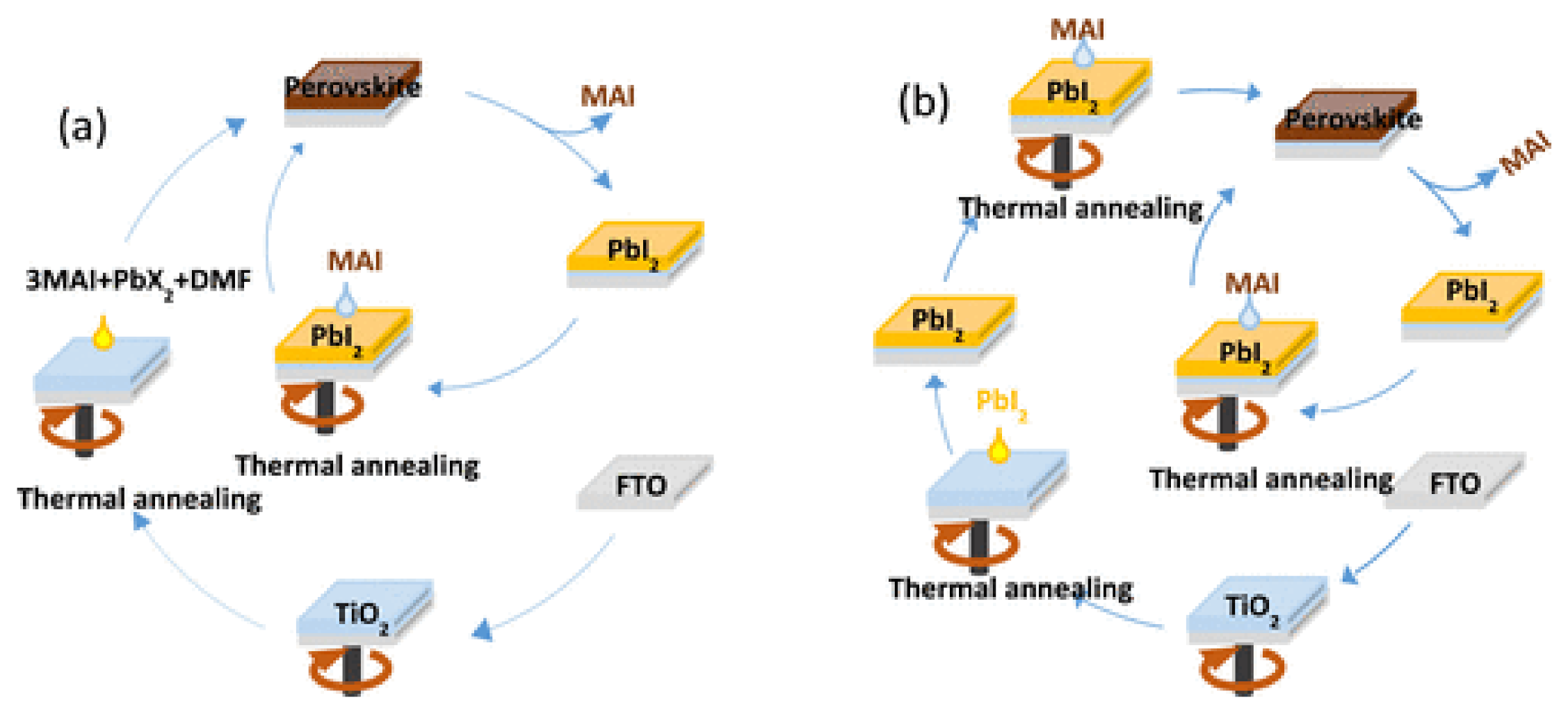
- Tong, G.; Son, D.-Y.; Ono, L.K.; Liu, Y.; Hu, Y.; Zhang, H.; Jamshaid, A.; Qiu, L.; Liu, Z.; Qi, Y. Scalable Fabrication of >90 cm(2) Perovskite Solar Modules with >1000 h Operational Stability Based on the Intermediate Phase Strategy. Adv. Energy Mater. 2021, 11, 2003712. [Google Scholar] [CrossRef]
- Li, S.; Hu, L.; Zhang, C.; Wu, Y.; Liu, Y.; Sun, Q.; Cui, Y.; Hao, Y.; Wu, Y. In situ growth of a 2D/3D mixed perovskite interface layer by seed-mediated and solvent-assisted Ostwald ripening for stable and efficient photovoltaics. J. Mater. Chem. C 2020, 8, 2425–2435. [Google Scholar] [CrossRef]
- Lin, Y.; Bai, Y.; Fang, Y.; Chen, Z.; Yang, S.; Zheng, X.; Tang, S.; Liu, Y.; Zhao, J.; Huang, J. Enhanced Thermal Stability in Perovskite Solar Cells by Assembling 2D/3D Stacking Structures. J. Phys. Chem. Lett. 2018, 9, 654–658. [Google Scholar] [CrossRef]
- Lee, J.W.; Dai, Z.; Han, T.H.; Choi, C.; Chang, S.Y.; Lee, S.J.; De Marco, N.; Zhao, H.; Sun, P.; Huang, Y.; et al. 2D perovskite stabilized phase-pure formamidinium perovskite solar cells. Nat. Commun. 2018, 9, 3021. [Google Scholar] [CrossRef] [Green Version]
- Kim, D.; Jung, H.J.; Park, I.J.; Larson, B.W.; Dunfield, S.P.; Xiao, C.; Kim, J.; Tong, J.; Boonmongkolras, P.; Ji, S.G.; et al. Efficient, stable silicon tandem cells enabled by anion-engineered wide-bandgap perovskites. Science 2020, 368, 155–160. [Google Scholar] [CrossRef]
- Zheng, X.; Hou, Y.; Bao, C.; Yin, J.; Yuan, F.; Huang, Z.; Song, K.; Liu, J.; Troughton, J.; Gasparini, N.; et al. Managing grains and interfaces via ligand anchoring enables 22.3%-efficiency inverted perovskite solar cells. Nat. Energy 2020, 5, 131–140. [Google Scholar] [CrossRef]
- Liu, W.; Chu, L.; Liu, N.; Ma, Y.; Hu, R.; Weng, Y.; Li, H.; Zhang, J.; Li, X.; Huang, W. Efficient perovskite solar cells fabricated by manganese cations incorporated in hybrid perovskites. J. Mater. Chem. C 2019, 7, 11943–11952. [Google Scholar] [CrossRef]
- Shai, X.; Wang, J.; Sun, P.; Huang, W.; Liao, P.; Cheng, F.; Zhu, B.; Chang, S.-Y.; Yao, E.-P.; Shen, Y.; et al. Achieving ordered and stable binary metal perovskite via strain engineering. Nano Energy 2018, 48, 117–127. [Google Scholar] [CrossRef]
- Qin, P.; Wu, T.; Wang, Z.; Xiao, L.; Ma, L.; Ye, F.; Xiong, L.; Chen, X.; Li, H.; Yu, X.; et al. Grain Boundary and Interface Passivation with Core–Shell Au@CdS Nanospheres for High-Efficiency Perovskite Solar Cells. Adv. Funct. Mater. 2020, 30, 1908408. [Google Scholar] [CrossRef]
- Sha, Y.; Bi, E.; Zhang, Y.; Ru, P.; Kong, W.; Zhang, P.; Yang, X.; Chen, H.; Han, L. A Scalable Integrated Dopant-Free Heterostructure to Stabilize Perovskite Solar Cell Modules. Adv. Energy Mater. 2021, 11, 2003301. [Google Scholar] [CrossRef]
- Yu, J.C.; Hong, J.A.; Jung, E.D.; Kim, D.B.; Baek, S.-M.; Lee, S.; Cho, S.; Park, S.S.; Choi, K.J.; Song, M.H. Highly efficient and stable inverted perovskite solar cell employing PEDOT: GO composite layer as a hole transport layer. Sci. Rep. 2018, 8, 1–9. [Google Scholar]
- Yu, J.C.; Badgujar, S.; Jung, E.D.; Singh, V.K.; Kim, D.W.; Gierschner, J.; Lee, E.; Kim, Y.S.; Cho, S.; Kwon, M.S.; et al. Highly Efficient and Stable Inverted Perovskite Solar Cell Obtained via Treatment by Semiconducting Chemical Additive. Adv. Mater. 2019, 31, e1805554. [Google Scholar] [CrossRef]
- Lee, Y.I.; Jeon, N.J.; Kim, B.J.; Shim, H.; Yang, T.-Y.; Seok, S.I.; Seo, J.; Im, S.G. A Low-Temperature Thin-Film Encapsulation for Enhanced Stability of a Highly Efficient Perovskite Solar Cell. Adv. Energy Mater. 2018, 8, 1701928. [Google Scholar] [CrossRef]
- Ouedraogo, N.A.N.; Chen, Y.; Xiao, Y.Y.; Meng, Q.; Han, C.B.; Yan, H.; Zhang, Y. Stability of all-inorganic perovskite solar cells. Nano Energy 2020, 67, 104249. [Google Scholar] [CrossRef]
- Liang, J.; Zhao, P.; Wang, C.; Wang, Y.; Hu, Y.; Zhu, G.; Ma, L.; Liu, J.; Jin, Z. CsPb0.9Sn0.1IBr2 Based All-Inorganic Perovskite Solar Cells with Exceptional Efficiency and Stability. J. Am. Chem. Soc. 2017, 139, 14009–14012. [Google Scholar] [CrossRef]
- Tan, X.; Liu, X.; Liu, Z.; Sun, B.; Li, J.; Xi, S.; Shi, T.; Tang, Z.; Liao, G. Enhancing the optical, morphological and electronic properties of the solution-processed CsPbIBr2 films by Li doping for efficient carbon-based perovskite solar cells. Appl. Surf. Sci. 2020, 499, 143990. [Google Scholar] [CrossRef]
- Xiang, W.; Wang, Z.; Kubicki, D.J.; Tress, W.; Luo, J.; Prochowicz, D.; Akin, S.; Emsley, L.; Zhou, J.; Dietler, G.; et al. Europium-Doped CsPbI2Br for Stable and Highly Efficient Inorganic Perovskite Solar Cells. Joule 2019, 3, 205–214. [Google Scholar] [CrossRef]
- Wang, Z.; Gan, J.; Liu, X.; Shi, H.; Wei, Q.; Zeng, Q.; Qiao, L.; Zheng, Y. Over 1 μm electron-hole diffusion lengths in CsPbI2Br for high efficient solar cells. J. Power Sources 2020, 454, 227913. [Google Scholar] [CrossRef]
- Wu, S.; Chen, R.; Zhang, S.; Babu, B.H.; Yue, Y.; Zhu, H.; Yang, Z.; Chen, C.; Chen, W.; Huang, Y. A chemically inert bismuth interlayer enhances long-term stability of inverted perovskite solar cells. Nat. Commun. 2019, 10, 1161. [Google Scholar] [CrossRef] [Green Version]
- Luo, Q.; Ma, H.; Hou, Q.; Li, Y.; Ren, J.; Dai, X.; Yao, Z.; Zhou, Y.; Xiang, L.; Du, H.; et al. All-Carbon-Electrode-Based Endurable Flexible Perovskite Solar Cells. Adv. Funct. Mater. 2018, 28, 1706777. [Google Scholar] [CrossRef]
- Jiang, X.; Yu, Z.; Li, H.-B.; Zhao, Y.; Qu, J.; Lai, J.; Ma, W.; Wang, D.; Yang, X.; Sun, L. A solution-processable copper(ii) phthalocyanine derivative as a dopant-free hole-transporting material for efficient and stable carbon counter electrode-based perovskite solar cells. J. Mater. Chem. A 2017, 5, 17862–17866. [Google Scholar] [CrossRef]
- Nie, W.; Blancon, J.C.; Neukirch, A.J.; Appavoo, K.; Tsai, H.; Chhowalla, M.; Alam, M.A.; Sfeir, M.Y.; Katan, C.; Even, J.; et al. Light-activated photocurrent degradation and self-healing in perovskite solar cells. Nat. Commun. 2016, 7, 11574. [Google Scholar] [CrossRef] [PubMed] [Green Version]
- Jeong, K.; Byeon, J.; Jang, J.; Ahn, N.; Choi, M.J. Pulsatile therapy for perovskite solar cells. arXiv 2020, arXiv:2007.06190. Available online: https://ui.adsabs.harvard.edu/abs/2020arXiv200706190J (accessed on 1 July 2020).
- Zhang, H.; Xiao, J.; Shi, J.; Su, H.; Luo, Y.; Li, D.; Wu, H.; Cheng, Y.-B.; Meng, Q. Self-Adhesive Macroporous Carbon Electrodes for Efficient and Stable Perovskite Solar Cells. Adv. Funct. Mater. 2018, 28, 1802985. [Google Scholar] [CrossRef]
- Ramasamy, E.; Karthikeyan, V.; Rameshkumar, K.; Veerappan, G. Glass-to-glass encapsulation with ultraviolet light curable epoxy edge sealing for stable perovskite solar cells. Mater. Lett. 2019, 250, 51–54. [Google Scholar] [CrossRef]
- Fu, Z.; Xu, M.; Sheng, Y.; Yan, Z.; Meng, J.; Tong, C.; Li, D.; Wan, Z.; Ming, Y.; Mei, A.; et al. Encapsulation of Printable Mesoscopic Perovskite Solar Cells Enables High Temperature and Long-Term Outdoor Stability. Adv. Funct. Mater. 2019, 29, 1809129. [Google Scholar] [CrossRef]
- Cheacharoen, R.; Boyd, C.C.; Burkhard, G.F.; Leijtens, T.; Raiford, J.A.; Bush, K.A.; Bent, S.F.; McGehee, M.D. Encapsulating perovskite solar cells to withstand damp heat and thermal cycling. Sustain. Energy Fuels 2018, 2, 2398–2406. [Google Scholar] [CrossRef]
- Shi, L.; Young, T.L.; Kim, J.; Sheng, Y.; Wang, L.; Chen, Y.; Feng, Z.; Keevers, M.J.; Hao, X.; Verlinden, P.J.; et al. Accelerated Lifetime Testing of Organic-Inorganic Perovskite Solar Cells Encapsulated by Polyisobutylene. ACS Appl. Mater. Interfaces 2017, 9, 25073–25081. [Google Scholar] [CrossRef]
- Dong, Q.; Liu, F.; Wong, M.K.; Tam, H.W.; Djurisic, A.B.; Ng, A.; Surya, C.; Chan, W.K.; Ng, A.M. Encapsulation of Perovskite Solar Cells for High Humidity Conditions. ChemSusChem 2016, 9, 2597–2603. [Google Scholar] [CrossRef]
- Alberti, A.; Deretzis, I.; Mannino, G.; Smecca, E.; Giannazzo, F.; Listorti, A.; Colella, S.; Masi, S.; Magna, A. Nitrogen Soaking Promotes Lattice Recovery in Polycrystalline Hybrid Perovskites. Adv. Energy Mater. 2019, 9, 1803450. [Google Scholar] [CrossRef]
- Wang, C.; Tan, G.; Luo, X.; Li, J.; Gao, X.; Mo, Y.; Zhang, X.-L.; Wang, X.; Huang, F. How to fabricate efficient perovskite solar mini-modules in lab. J. Power Sources 2020, 466, 228321. [Google Scholar] [CrossRef]
- Wei, M.; Xiao, K.; Walters, G.; Lin, R.; Zhao, Y.; Saidaminov, M.I.; Todorovic, P.; Johnston, A.; Huang, Z.; Chen, H.; et al. Combining Efficiency and Stability in Mixed Tin-Lead Perovskite Solar Cells by Capping Grains with an Ultrathin 2D Layer. Adv. Mater. 2020, 32, e1907058. [Google Scholar] [CrossRef]
- Leijtens, T.; Prasanna, R.; Bush, K.A.; Eperon, G.E.; Raiford, J.A.; Gold-Parker, A.; Wolf, E.J.; Swifter, S.A.; Boyd, C.C.; Wang, H.-P. Tin–lead halide perovskites with improved thermal and air stability for efficient all-perovskite tandem solar cells. Sustain. Energy Fuels 2018, 2, 2450–2459. [Google Scholar] [CrossRef]
- Jung, E.H.; Jeon, N.J.; Park, E.Y.; Moon, C.S.; Shin, T.J.; Yang, T.Y.; Noh, J.H.; Seo, J. Efficient, stable and scalable perovskite solar cells using poly(3-hexylthiophene). Nature 2019, 567, 511–515. [Google Scholar] [CrossRef]
- Lim, K.-S.; Lee, D.-K.; Lee, J.-W.; Park, N.-G. 17% efficient perovskite solar mini-module via hexamethylphosphoramide (HMPA)-adduct-based large-area D-bar coating. J. Mater. Chem. A 2020, 8, 9345–9354. [Google Scholar] [CrossRef]
- Ma, Z.; Xiao, Z.; Zhou, W.; Jin, L.; Huang, D.; Jiang, H.; Yang, T.; Liu, Y.; Huang, Y. Efficient CH3NH3PbI3-x (SeCN) x perovskite solar cells with improved crystallization and defect passivation. J. Alloy. Compd. 2020, 822, 153539. [Google Scholar] [CrossRef]
- Zhao, X.; Yao, C.; Liu, T.; Hamill, J.C., Jr.; Ngongang Ndjawa, G.O.; Cheng, G.; Yao, N.; Meng, H.; Loo, Y.L. Extending the photovoltaic response of perovskite solar cells into the near-infrared with a narrow-bandgap organic semiconductor. Adv. Mater. 2019, 31, 1904494. [Google Scholar] [CrossRef]
- Wang, H.; Wang, Z.; Yang, Z.; Xu, Y.; Ding, Y.; Tan, L.; Yi, C.; Zhang, Z.; Meng, K.; Chen, G.; et al. Ligand-Modulated Excess PbI2 Nanosheets for Highly Efficient and Stable Perovskite Solar Cells. Adv. Mater. 2020, 32, e2000865. [Google Scholar] [CrossRef]
- Babayigit, A.; Ethirajan, A.; Muller, M.; Conings, B. Toxicity of organometal halide perovskite solar cells. Nat. Mater. 2016, 15, 247–251. [Google Scholar] [CrossRef]
- Jiang, Y.; Qiu, L.; Juarez-Perez, E.J.; Ono, L.K.; Hu, Z.; Liu, Z.; Wu, Z.; Meng, L.; Wang, Q.; Qi, Y. Reduction of lead leakage from damaged lead halide perovskite solar modules using self-healing polymer-based encapsulation. Nat. Energy 2019, 4, 585–593. [Google Scholar] [CrossRef]
- Du, K.Z.; Meng, W.; Wang, X.; Yan, Y.; Mitzi, D.B. Bandgap Engineering of Lead-Free Double Perovskite Cs2 AgBiBr6 through Trivalent Metal Alloying. Angew. Chem. Int. Ed. 2017, 56, 8158–8162. [Google Scholar] [CrossRef]
- Wang, M.; Zeng, P.; Bai, S.; Gu, J.; Li, F.; Yang, Z.; Liu, M. High-Quality Sequential-Vapor-Deposited Cs2AgBiBr6 Thin Films for Lead-Free Perovskite Solar Cells. Sol. RRL 2018, 2, 1800217. [Google Scholar] [CrossRef]
- Zhang, Z.; Li, X.; Xia, X.; Wang, Z.; Huang, Z.; Lei, B.; Gao, Y. High-Quality (CH3NH3)3Bi2I9 Film-Based Solar Cells: Pushing Efficiency up to 1.64. J. Phys. Chem. Lett. 2017, 8, 4300–4307. [Google Scholar] [CrossRef] [PubMed]
- Chen, M.; Ju, M.G.; Garces, H.F.; Carl, A.D.; Ono, L.K.; Hawash, Z.; Zhang, Y.; Shen, T.; Qi, Y.; Grimm, R.L.; et al. Highly stable and efficient all-inorganic lead-free perovskite solar cells with native-oxide passivation. Nat. Commun. 2019, 10, 16. [Google Scholar] [CrossRef] [PubMed] [Green Version]
- Dang, Y.; Zhou, Y.; Liu, X.; Ju, D.; Xia, S.; Xia, H.; Tao, X. Formation of Hybrid Perovskite Tin Iodide Single Crystals by Top-Seeded Solution Growth. Angew. Chem. Int. Ed. 2016, 55, 3447–3450. [Google Scholar] [CrossRef]
- He, X.; Wu, T.; Liu, X.; Wang, Y.; Meng, X.; Wu, J.; Noda, T.; Yang, X.; Moritomo, Y.; Segawa, H.; et al. Highly efficient tin perovskite solar cells achieved in a wide oxygen concentration range. J. Mater. Chem. A 2020, 8, 2760–2768. [Google Scholar] [CrossRef]
- Nishimura, K.; Kamarudin, M.A.; Hirotani, D.; Hamada, K.; Shen, Q.; Iikubo, S.; Minemoto, T.; Yoshino, K.; Hayase, S. Lead-free tin-halide perovskite solar cells with 13% efficiency. Nano Energy 2020, 74, 104858. [Google Scholar] [CrossRef]
- Shao, S.; Liu, J.; Portale, G.; Fang, H.-H.; Blake, G.R.; ten Brink, G.H.; Koster, L.J.A.; Loi, M.A. Highly Reproducible Sn-Based Hybrid Perovskite Solar Cells with 9% Efficiency. Adv. Energy Mater. 2018, 8, 1702019. [Google Scholar] [CrossRef]
- Chen, Q.; Luo, J.; He, R.; Lai, H.; Ren, S.; Jiang, Y.; Wan, Z.; Wang, W.; Hao, X.; Wang, Y.; et al. Unveiling Roles of Tin Fluoride Additives in High-Efficiency Low-Bandgap Mixed Tin-Lead Perovskite Solar Cells. Adv. Energy Mater. 2021, 11, 2101045. [Google Scholar] [CrossRef]
- Chen, M.; Ju, M.-G.; Carl, A.D.; Zong, Y.; Grimm, R.L.; Gu, J.; Zeng, X.C.; Zhou, Y.; Padture, N.P. Cesium Titanium(IV) Bromide Thin Films Based Stable Lead-free Perovskite Solar Cells. Joule 2018, 2, 558–570. [Google Scholar] [CrossRef] [Green Version]
- Ju, M.-G.; Chen, M.; Zhou, Y.; Garces, H.F.; Dai, J.; Ma, L.; Padture, N.P.; Zeng, X.C. Earth-Abundant Nontoxic Titanium(IV)-based Vacancy-Ordered Double Perovskite Halides with Tunable 1.0 to 1.8 eV Bandgaps for Photovoltaic Applications. ACS Energy Lett. 2018, 3, 297–304. [Google Scholar] [CrossRef]
- Park, N.-G.; Grätzel, M.; Miyasaka, T.; Zhu, K.; Emery, K. Towards stable and commercially available perovskite solar cells. Nat. Energy 2016, 1, 16152. [Google Scholar] [CrossRef]
- Berry, J.J.; van de Lagemaat, J.; Al-Jassim, M.M.; Kurtz, S.; Yan, Y.; Zhu, K. Perovskite Photovoltaics: The Path to a Printable Terawatt-Scale Technology. ACS Energy Lett. 2017, 2, 2540–2544. [Google Scholar] [CrossRef]
- Ahn, N.; Son, D.Y.; Jang, I.H.; Kang, S.M.; Choi, M.; Park, N.G. Highly Reproducible Perovskite Solar Cells with Average Efficiency of 18.3% and Best Efficiency of 19.7% Fabricated via Lewis Base Adduct of Lead(II) Iodide. J. Am. Chem. Soc. 2015, 137, 8696–8699. [Google Scholar] [CrossRef]
- Nie, W.; Tsai, H.; Asadpour, R.; Blancon, J.C.; Neukirch, A.J.; Gupta, G.; Crochet, J.J.; Chhowalla, M.; Tretiak, S.; Alam, M.A.; et al. High-efficiency solution-processed perovskite solar cells with millimeter-scale grains. Science 2015, 347, 522–525. [Google Scholar] [CrossRef] [Green Version]
- Kim, D.H.; Park, J.; Li, Z.; Yang, M.; Park, J.S.; Park, I.J.; Kim, J.Y.; Berry, J.J.; Rumbles, G.; Zhu, K. 300% Enhancement of Carrier Mobility in Uniaxial-Oriented Perovskite Films Formed by Topotactic-Oriented Attachment. Adv. Mater. 2017, 29, 1606831. [Google Scholar] [CrossRef]
- Shen, D.; Yu, X.; Cai, X.; Peng, M.; Ma, Y.; Su, X.; Xiao, L.; Zou, D. Understanding the solvent-assisted crystallization mechanism inherent in efficient organic–inorganic halide perovskite solar cells. J. Mater. Chem. A 2014, 2, 20454–20461. [Google Scholar] [CrossRef]
- Lv, M.; Dong, X.; Fang, X.; Lin, B.; Zhang, S.; Ding, J.; Yuan, N. A promising alternative solvent of perovskite to induce rapid crystallization for high-efficiency photovoltaic devices. RSC Adv. 2015, 5, 20521–20529. [Google Scholar] [CrossRef]
- Yang, M.; Kim, D.H.; Klein, T.R.; Li, Z.; Reese, M.O.; Tremolet de Villers, B.J.; Berry, J.J.; van Hest, M.F.A.M.; Zhu, K. Highly Efficient Perovskite Solar Modules by Scalable Fabrication and Interconnection Optimization. ACS Energy Lett. 2018, 3, 322–328. [Google Scholar] [CrossRef]
- Hsieh, T.Y.; Wei, T.C.; Wu, K.L.; Ikegami, M.; Miyasaka, T. Efficient perovskite solar cells fabricated using an aqueous lead nitrate precursor. Chem. Commun. 2015, 51, 13294–13297. [Google Scholar] [CrossRef]
- Kosta, I.; Grande, H.; Tena-Zaera, R. Dimethylformamide-free processing of halide perovskite solar cells from electrodeposited PbI2 precursor films. Electrochim. Acta 2017, 246, 1193–1199. [Google Scholar] [CrossRef]
- Sveinbjörnsson, K.; Kyi Thein, N.K.; Saki, Z.; Svanström, S.; Yang, W.; Cappel, U.B.; Rensmo, H.; Boschloo, G.; Aitola, K.; Johansson, E.M.J. Preparation of mixed-ion and inorganic perovskite films using water and isopropanol as solvents for solar cell applications. Sustain. Energy Fuels 2018, 2, 606–615. [Google Scholar] [CrossRef]
- Gardner, K.L.; Tait, J.G.; Merckx, T.; Qiu, W.; Paetzold, U.W.; Kootstra, L.; Jaysankar, M.; Gehlhaar, R.; Cheyns, D.; Heremans, P.; et al. Nonhazardous Solvent Systems for Processing Perovskite Photovoltaics. Adv. Energy Mater. 2016, 6, 1600386. [Google Scholar] [CrossRef]
- Noel, N.K.; Habisreutinger, S.N.; Wenger, B.; Klug, M.T.; Hörantner, M.T.; Johnston, M.B.; Nicholas, R.J.; Moore, D.T.; Snaith, H.J. A low viscosity, low boiling point, clean solvent system for the rapid crystallisation of highly specular perovskite films. Energy Environ. Sci. 2017, 10, 145–152. [Google Scholar] [CrossRef]
- Cai, M.; Wu, Y.; Chen, H.; Yang, X.; Qiang, Y.; Han, L. Cost-Performance Analysis of Perovskite Solar Modules. Adv. Sci. 2017, 4, 1600269. [Google Scholar] [CrossRef]
- Binek, A.; Petrus, M.L.; Huber, N.; Bristow, H.; Hu, Y.; Bein, T.; Docampo, P. Recycling Perovskite Solar Cells To Avoid Lead Waste. ACS Appl. Mater. Interfaces 2016, 8, 12881–12886. [Google Scholar] [CrossRef] [Green Version]
- Augustine, B.; Remes, K.; Lorite, G.S.; Varghese, J.; Fabritius, T. Recycling perovskite solar cells through inexpensive quality recovery and reuse of patterned indium tin oxide and substrates from expired devices by single solvent treatment. Sol. Energy Mater. Sol. Cells 2019, 194, 74–82. [Google Scholar] [CrossRef]
- Chhillar, P.; Dhamaniya, B.P.; Dutta, V.; Pathak, S.K. Recycling of Perovskite Films: Route toward Cost-Efficient and Environment-Friendly Perovskite Technology. ACS Omega 2019, 4, 11880–11887. [Google Scholar] [CrossRef] [Green Version]
- Chang, N.L.; Yi Ho-Baillie, A.W.; Basore, P.A.; Young, T.L.; Evans, R.; Egan, R.J. A manufacturing cost estimation method with uncertainty analysis and its application to perovskite on glass photovoltaic modules. Prog. Photovolt. Res. Appl. 2017, 25, 390–405. [Google Scholar] [CrossRef]
- Song, Z.; McElvany, C.L.; Phillips, A.B.; Celik, I.; Krantz, P.W.; Watthage, S.C.; Liyanage, G.K.; Apul, D.; Heben, M.J. A technoeconomic analysis of perovskite solar module manufacturing with low-cost materials and techniques. Energy Environ. Sci. 2017, 10, 1297–1305. [Google Scholar] [CrossRef]


| Materials | Provider | Curing Condition | Appearance | Hardness (D) |
|---|---|---|---|---|
| UV-curable epoxy | ThreeBond | 60 kJ/m2, 80 °C, 1 h | pinkish white | 76 |
| AB epoxy glue | Super Glue Corp. | 25 °C, 4–6 min | Hazy white | 75–85 |
| Thermally curable epoxy | Kyoritsu Chemical | 6000 mJ/cm2, 80 °C, 30 min | —— | 83 |
| Materials | Provider | Transmittance (%) | Elastic Modulus (MPa) | Possibly Harmful |
|---|---|---|---|---|
| EVA | Mitsui Chemicals | 93 | 10 | Acetic acid |
| Surlyn | Dupont | 93.4 | 397 | Methacrylic acid |
| Polyolefin | 3M | 91 | 9.1 | Unknown |
| Perovskite Materials | Device Structure | Active Area/mm2 | Initial PCE (%) | Test Condition | Stability Result | Published Year | Ref. |
|---|---|---|---|---|---|---|---|
| Cs0.05(FA0.92MA0.08)0.95 Pb(I0.92Br0.08)3 | ITO/PTAA/PVSK /C60/BCP/Cu | 6.69 | 23 | MMP tracking on encapsulated devices under AM1.5 illumination for 1000 h | Negligible decrease | 2020 | [191] |
| T = 85 °C, for 1020 h in N2 environment | lost around 10% | ||||||
| Cs0.1MA0.2FA0.7Pb0.5Sn0.5I3 | ITO/ PEDOT:PSS/PVSK/PCBM/ PEIE/Ag | 4.9 | 18.95 | Under full AM1.5G illumination (without UV-filter) after 8.6 h | lost around 10% | 2020 | [192] |
| (Kx(Cs0.05(FA0.85MA0.15)0.95Pb(I0.85Br0.15)3 | FTO/SnO2/PVSK/Spiro-OMeTAD/Au | 16 | 20.56 | Unencapsulated devices stored under ambient air conditions with 10 ± 5 RH% over 1000 h | no decrease | 2017 | [160] |
| FA0.75Cs0.25Sn0.5Pb0.5I3 | ITO/ PEDOT:PSS/PVSK/C60/BCP/Ag | 15.6 | Under continuous one-sun illumination over 30 h | no decrease | 2018 | [193] | |
| Rb-FA0.75MA0.15Cs0.1PbI2Br | FTO/TiO2/PVSK/PTAA/Au | 17.64 | 17.4 | under continuous one-Sun illumination after >12 h under N2 environment and the T = 25 °C | lost around 5% | 2017 | [159] |
| Rb- Cs0.05(MA0.17FA0.83)0.95Pb(I0.83Br0.17)3 | ITO/TiO2/PVSK/PTAA/Au | 4 | 18.03 | Unencapsulated devices stored at 85 °C, under dry air (<5% humidity), after 347 h | lost around 26% | 2018 | [194] |
| (FA0.65MA0.20Cs0.15)Pb(I0.8Br0.2)3 | ITO/PTAA/PVSK/C60/ BCP/Ag | 6 | 19.8 | Stored at room temperature under N2 environment for over 4000 h | lost around 4% | 2019 | [195] |
| (FA0.65MA0.2Cs0.15)Pb(I0.8Br0.2)3 | ITO/PTAA/PVSK/C60/ BCP/Ag | 20.7 | Unencapsulated devices tested under continuous illumination in an N2-filled environment for 1000 h | lost around 20% | 2020 | [80] | |
| MAPbI3−x(SeCN)x | FTO/TiO2/PVSK/Spiro-oMeTAD/Ag | 16 | 18.41 | Placed in N2-filled glove box after continuous testing for 500 h (tested every 24 h) | lost around 14% | 2019 | [196] |
| (CsPbI3)0.04 (FAPbI3)0.82 (MAPbBr3)0.14 | FTO/SnO2/PVSK/Spiro-OMeTAD/Au | 9 | 21.38 | Test at room temperature and 70% humidity and stored in ≈25% humidity at RT in the dark over 1080 h without encapsulation | lost around 10% | 2020 | [126] |
| Cs0.05(MA0.17FA0.83)0.95Pb(I0.83Br0.17)3 | FTO/TiO2/PVSK/Spiro-OMeTAD/Au | 12 | 21.6 | Encapsulated devices under continuous one sun illumination (≈30 °C, ≈35% humidity) for 300 h | lost around 24% | 2019 | [197] |
| (FAPbI3)0.85 (MAPbBr3)0.15 | ITO/NiOx/PVSK/PCBM/ZrAcac/Ag | 7.5 | 20.67 | Encapsulated devices under continuous one-sun illumination (≈23 °C, ≈35% humidity) for 200 h | lost around 24% | 2019 | [127] |
| (FAPbI3)0.8 (MAPbBr3)0.2 | ITO/ PEDOT:PSS/PVSK/PCBM/ ZnO/Ag | 13.5 | 20.3 | unencapsulated devices tested under continuous one sun illumination (25 °C, 60% humidity) over 170 h | lost around 16% | 2018 | [171] |
| MAPb1−xMnxI3 | FTO/TiO2/PVSK/Spiro-OMeTAD/Ag | 9 | 19.09 | unencapsulated devices stored in an ambient atmosphere (30% relative humidity and 25 °C) for 48 h | lost around 5% | 2019 | [191] |
| Rb5Cs10FAPbI3 | FTO/SnO2/PCBM: PMMA/PVSK/PMMA/Spiro-OMeTAD/Au | 10.24 | 20.35 | 1000 h of continuous MMP tracking under N2 atmosphere at room temperature | lost around 2% | 2018 | [158] |
| (FAxMA1−x)Pb(IyCl1-y)3 | ITO/SnO2/PVSK/Spiro-OMeTAD/Au | 9 | 22.03 | unencapsulated devices stored in the atmosphere at 66% humidity after 110 h | lost around 22% | 2020 | [198] |
| (FAPbI3)1−x(MAPbBr3)x | FTO/TiO2/PVSK/Spiro-OMeTAD/Au | 19.3 | Stored at 25 °C with the humidity of 40% after 700 h, in dark | lost around 3% | 2019 | [114] | |
| MAPb(IxBr1−x)3 | ITO/ PEDOT:GO/PVSK/PCBM/ ZnO/Ag | 13.5 | 18.09 | encapsulated devices were measured under an ambient air condition after 25 days | lost around 20% | 2018 | [107] |
| MAPbI3−xClx | ITO/ PEDOT:PSS/PVSK/PCBM/ RhB101/Ag/LiF | 11 | 18.0 | unencapsulated devices were stored in ambient environment with 55 ± 5% humidity after 240 h | lost around 50% | 2018 | [105] |
| MAPbIxCl3−x | ITO/PEDOT:SAF/PVSK/PCBM/BCP/Ag | 12.5 | 16.2 | unencapsulated devices were stored in ambient air with RH% ∼30% for 44 days without excluding the room light | lost around 10% | 2019 | [113] |
| MAPb(I0.9Br0.1)3 | FTO/NiO:5K/PVSK /PCBM/C60/BCP/Ag | 18.05 | unencapsulated devices were stored in ambient air with RH% 15 ± 5% for 240 h | lost around 10% | 2019 | [140] |
Publisher’s Note: MDPI stays neutral with regard to jurisdictional claims in published maps and institutional affiliations. |
© 2021 by the authors. Licensee MDPI, Basel, Switzerland. This article is an open access article distributed under the terms and conditions of the Creative Commons Attribution (CC BY) license (https://creativecommons.org/licenses/by/4.0/).
Share and Cite
Wang, H.; Wang, Y.; Xuan, Z.; Chen, T.; Zhang, J.; Hao, X.; Wu, L.; Constantinou, I.; Zhao, D. Progress in Perovskite Solar Cells towards Commercialization—A Review. Materials 2021, 14, 6569. https://doi.org/10.3390/ma14216569
Wang H, Wang Y, Xuan Z, Chen T, Zhang J, Hao X, Wu L, Constantinou I, Zhao D. Progress in Perovskite Solar Cells towards Commercialization—A Review. Materials. 2021; 14(21):6569. https://doi.org/10.3390/ma14216569
Chicago/Turabian StyleWang, Hongqiao, Yunfan Wang, Zhipeng Xuan, Tingting Chen, Jingquan Zhang, Xia Hao, Lili Wu, Iordania Constantinou, and Dewei Zhao. 2021. "Progress in Perovskite Solar Cells towards Commercialization—A Review" Materials 14, no. 21: 6569. https://doi.org/10.3390/ma14216569
APA StyleWang, H., Wang, Y., Xuan, Z., Chen, T., Zhang, J., Hao, X., Wu, L., Constantinou, I., & Zhao, D. (2021). Progress in Perovskite Solar Cells towards Commercialization—A Review. Materials, 14(21), 6569. https://doi.org/10.3390/ma14216569