Cesium Doping for Performance Improvement of Lead(II)-acetate-Based Perovskite Solar Cells


Abstract
1. Introduction
2. Materials and Methods
2.1. Materials
2.2. Device Fabrication
2.3. Measurements
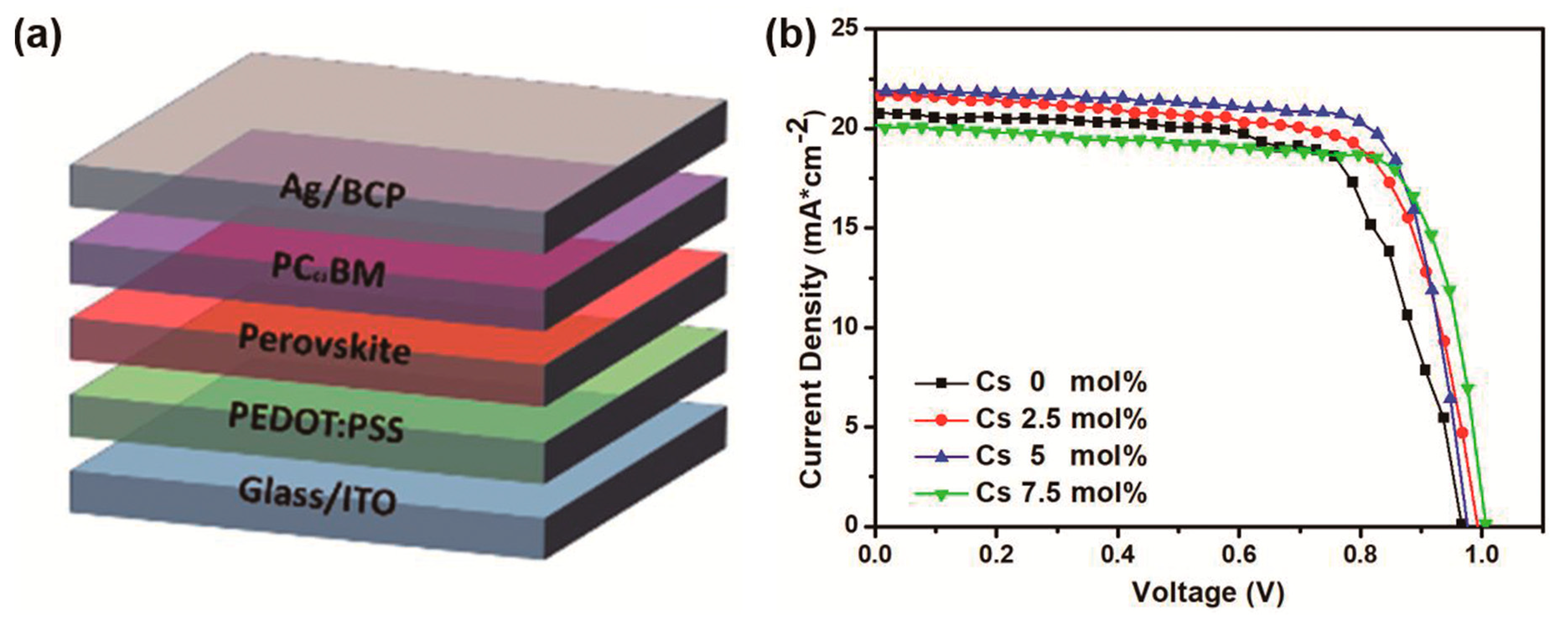
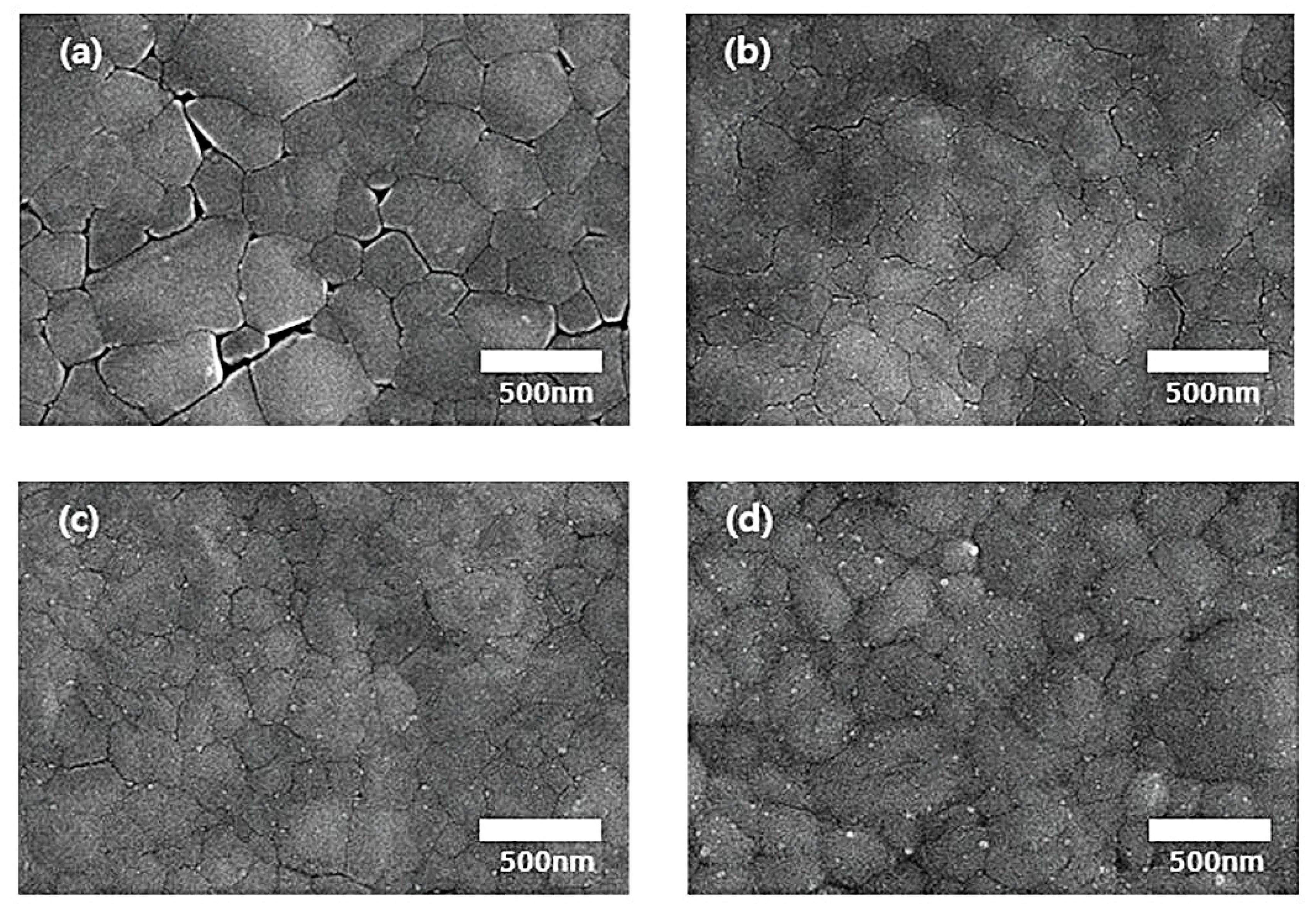
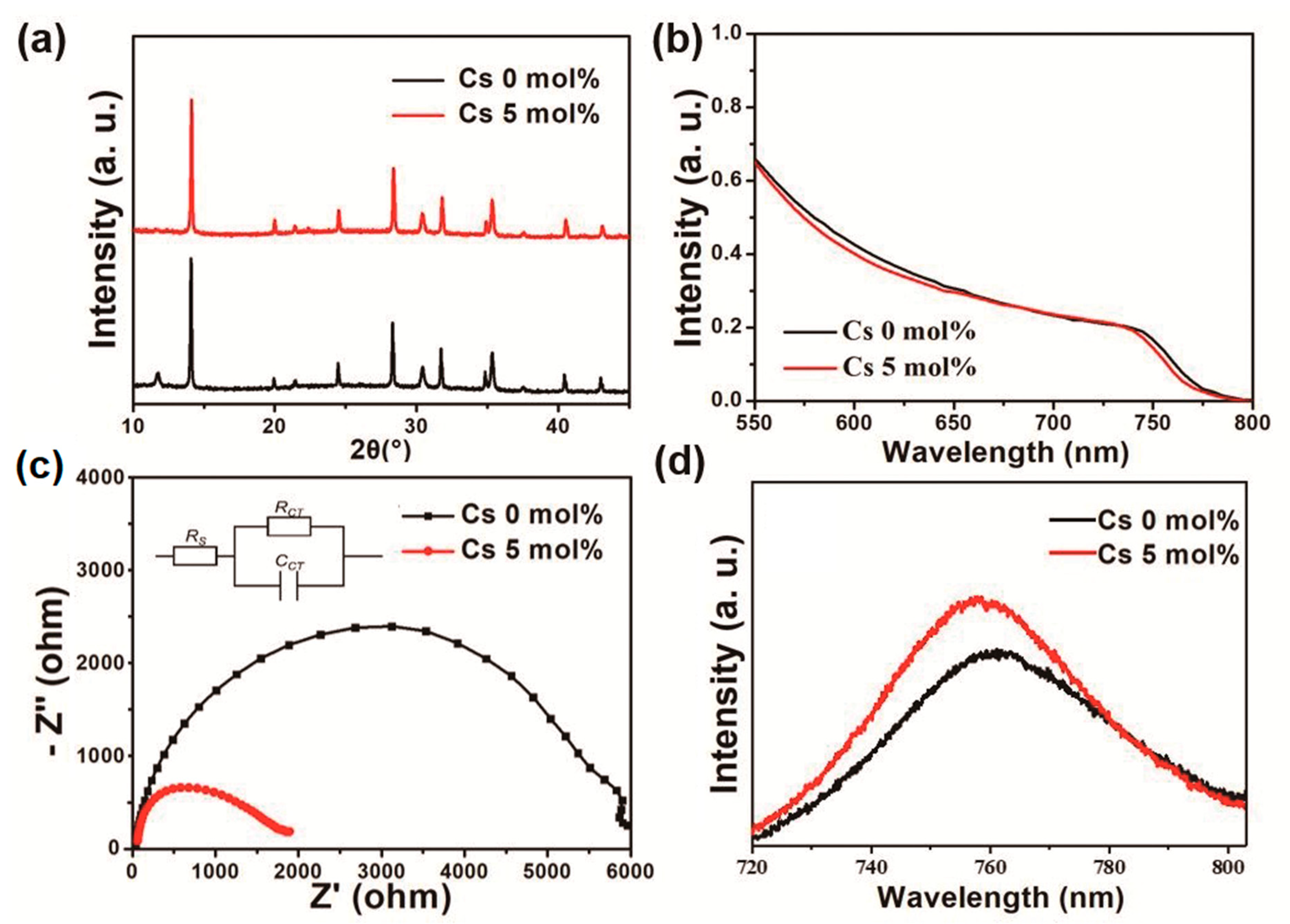
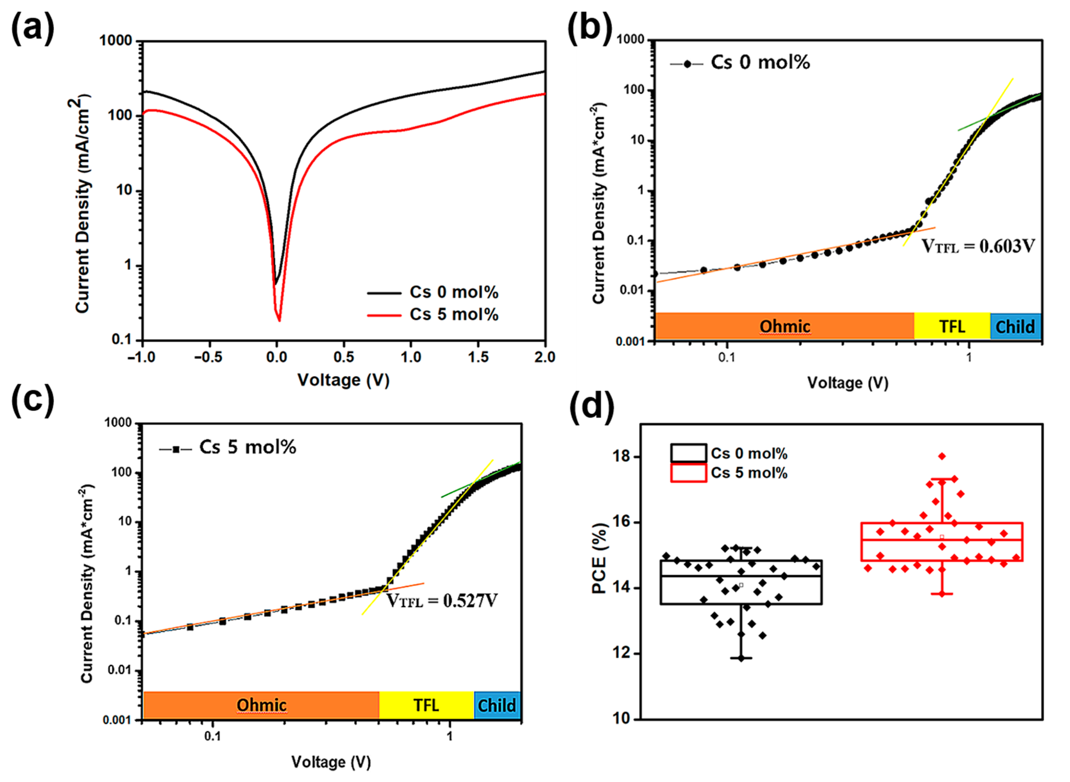
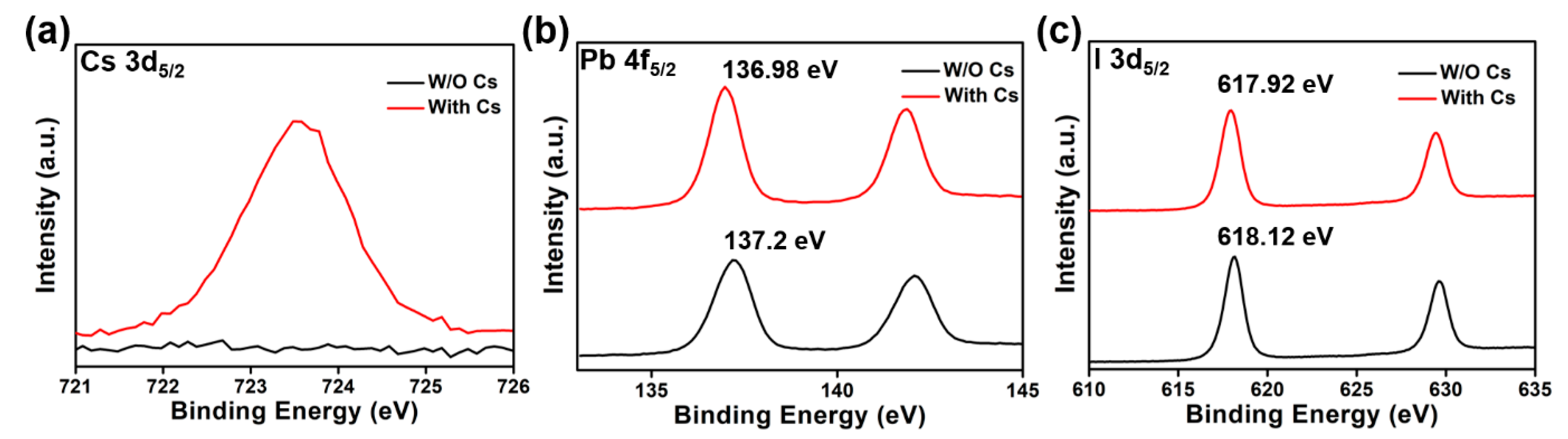
3. Results
4. Summary
Supplementary Materials
Author Contributions
Funding
Data Availability Statement
Conflicts of Interest
References
- Stranks, S.D.; Eperon, G.E.; Grancini, G.; Menelaou, C.; Alcocer, M.J.; Leijtens, T.; Herz, L.M.; Petrozza, A.; Snaith, H.J. Electron-hole diffusion lengths exceeding 1 micrometer in an organometal trihalide perovskite absorber. Science 2013, 342, 341–344. [Google Scholar] [CrossRef] [PubMed]
- Kojima, A.; Teshima, K.; Shirai, Y.; Miyasaka, T. Organometal Halide Perovskites as Visible-Light Sensitizers for Photovoltaic Cells. J. Am. Chem. Soc. 2009, 131, 6050–6051. [Google Scholar] [CrossRef] [PubMed]
- Burschka, J.; Pellet, N.; Moon, S.J.; Humphry-Baker, R.; Gao, P.; Nazeeruddin, M.K.; Gratzel, M. Sequential deposition as a route to high-performance perovskite-sensitized solar cells. Nature 2013, 499, 316–319. [Google Scholar] [CrossRef] [PubMed]
- Zhou, H.; Chen, Q.; Li, G.; Luo, S.; Song, T.B.; Duan, H.S.; Hong, Z.; You, J.; Liu, Y.; Yang, Y. Photovoltaics. Interface engineering of highly efficient perovskite solar cells. Science 2014, 345, 542–546. [Google Scholar] [CrossRef] [PubMed]
- Jeon, N.J.; Noh, J.H.; Yang, W.S.; Kim, Y.C.; Ryu, S.; Seo, J.; Seok, S.I. Compositional engineering of perovskite materials for high-performance solar cells. Nature 2015, 517, 476–480. [Google Scholar] [CrossRef] [PubMed]
- Bi, D.; Yi, C.; Luo, J.; Décoppet, J.-D.; Zhang, F.; Zakeeruddin, S.M.; Li, X.; Hagfeldt, A.; Grätzel, M. Polymer-templated nucleation and crystal growth of perovskite films for solar cells with efficiency greater than 21%. Nat. Energy. 2016, 1, 16142. [Google Scholar] [CrossRef]
- Sahli, F.; Werner, J.; Kamino, B.A.; Brauninger, M.; Monnard, R.; Paviet-Salomon, B.; Barraud, L.; Ding, L.; Diaz Leon, J.J.; Sacchetto, D.; et al. Fully textured monolithic perovskite/silicon tandem solar cells with 25.2% power conversion efficiency. Nat Mater 2018, 17, 820–826. [Google Scholar] [CrossRef]
- NREL. Best Research-Cell Efficiency Chart| Photovoltaic Research| NREL. 2019. Available online: https://www.nrel.gov/pv/cell-efficiency.html (accessed on 13 January 2021).
- Kim, H.-S.; Lee, C.-R.; Im, J.-H.; Lee, K.-B.; Moehl, T.; Marchioro, A.; Moon, S.-J.; Humphry-Baker, R.; Yum, J.-H.; Moser, J.E. Lead iodide perovskite sensitized all-solid-state submicron thin film mesoscopic solar cell with efficiency exceeding 9%. Scientific reports 2012, 2, 1–7. [Google Scholar] [CrossRef]
- Paek, S.; Schouwink, P.; Athanasopoulou, E.N.; Cho, K.T.; Grancini, G.; Lee, Y.; Zhang, Y.; Stellacci, F.; Nazeeruddin, M.K.; Gao, P. From nano- to micrometer scale: The role of antisolvent treatment on high performance perovskite solar cells. Chem. Mater. 2017, 29, 3490–3498. [Google Scholar] [CrossRef]
- Tavakoli, M.M.; Yadav, P.; Prochowicz, D.; Sponseller, M.; Osherov, A.; Bulović, V.; Kong, J. Controllable perovskite crystallization via antisolvent technique using chloride additives for highly efficient planar perovskite solar cells. Adv. Energy Mater. 2019, 9, 1803587. [Google Scholar] [CrossRef]
- Pool, V.L.; Gold-Parker, A.; McGehee, M.D.; Toney, M.F. Chlorine in PbCl2-derived hybrid-perovskite solar absorbers. Chem. Mater. 2015, 27, 7240–7243. [Google Scholar] [CrossRef]
- Zhang, W.; Saliba, M.; Moore, D.T.; Pathak, S.K.; Hörantner, M.T.; Stergiopoulos, T.; Stranks, S.D.; Eperon, G.E.; Alexander-Webber, J.A.; Abate, A.; et al. Ultrasmooth organic–inorganic perovskite thin-film formation and crystallization for efficient planar heterojunction solar cells. Nat. Commun. 2015, 6, 1–10. [Google Scholar]
- Zhang, F.; Zhu, K. Additive engineering for efficient and stable perovskite solar cells. Adv. Energy Mater. 2020, 10, 1902579. [Google Scholar] [CrossRef]
- Liu, Y.; Liu, Z.; Lee, E.-C. Dimethyl-sulfoxide-assisted improvement in the crystallization of lead-acetate-based perovskites for high-performance solar cells. J. Mater. Chem. C 2018, 6, 6705–6713. [Google Scholar] [CrossRef]
- Saliba, M.; Matsui, T.; Seo, J.-Y.; Domanski, K.; Correa-Baena, J.-P.; Nazeeruddin, M.K.; Zakeeruddin, S.M.; Tress, W.; Abate, A.; Hagfeldt, A.; et al. Cesium-containing triple cation perovskite solar cells: Improved stability, reproducibility and high efficiency. Energy Environ. Sci. 2016, 9, 1989–1997. [Google Scholar] [CrossRef] [PubMed]
- Nemnes, G.A.; Besleaga, C.; Tomulescu, A.G.; Palici, A.; Pintilie, L.; Manolescu, A.; Pintilie, I. How measurement protocols influence the dynamic JV characteristics of perovskite solar cells: Theory and experiment. Sol. Energy 2018, 173, 976–983. [Google Scholar] [CrossRef]
- Liu, W.; Liu, N.; Ji, S.; Hua, H.; Ma, Y.; Hu, R.; Zhang, J.; Chu, L.; Li, X.; Huang, W. Perfection of perovskite grain boundary passivation by rhodium incorporation for efficient and stable solar cells. Nano-Micro Lett. 2020, 12, 119. [Google Scholar] [CrossRef]
- Li, S.-S.; Chang, C.-H.; Wang, Y.-C.; Lin, C.-W.; Wang, D.-Y.; Lin, J.-C.; Chen, C.-C.; Sheu, H.-S.; Chia, H.-C.; Wu, W.-R.; et al. Intermixing-seeded growth for high-performance planar heterojunction perovskite solar cells assisted by precursor-capped nanoparticles. Energy Environ. Sci. 2016, 9, 1282–1289. [Google Scholar] [CrossRef]
- Sewvandi, G.A.; Hu, D.; Chen, C.; Ma, H.; Kusunose, T.; Tanaka, Y.; Nakanishi, S.; Feng, Q. Antiferroelectric-to-ferroelectric switching in CH3NH3PbI3 perovskite and its potential role in effective charge separation in perovskite solar cells. Phys. Rev. Appl. 2016, 6, 24007. [Google Scholar] [CrossRef]
- Gausin, C.M. Improved Thermal Stability of Cesium-Doped Perovskite Films with PMMA for Solar Cell Application. Master’s Thesis, Old Dominion University, Norfolk, VA, USA, 2018. [Google Scholar]
- Drahansky, M.; Paridah, M.; Moradbak, A.; Mohamed, A.; Owolabi, F.; Asniza, M. We are IntechOpen, the world’s leading publisher of Open Access books Built by scientists, for scientists TOP 1%. Intech 2016, 1, 13. [Google Scholar]
- Wu, C.; Guo, D.; Li, P.; Wang, S.; Liu, A.; Wu, F. A study on the effects of mixed organic cations on the structure and properties in lead halide perovskites. Phys. Chem. Chem. Phys. 2020, 22, 3105–3111. [Google Scholar] [CrossRef]
- Yang, D.; Zhou, X.; Yang, R.; Yang, Z.; Yu, W.; Wang, X.; Li, C.; Liu, S.; Chang, R.P.H. Surface optimization to eliminate hysteresis for record efficiency planar perovskite solar cells. Energy Environ. Sci. 2016, 9, 3071–3078. [Google Scholar] [CrossRef]
- Yang, D.; Yang, R.; Zhang, J.; Yang, Z.; Liu, S.; Li, C. High efficiency flexible perovskite solar cells using superior low temperature TiO2. Energy Environ. Sci. 2015, 8, 3208–3214. [Google Scholar] [CrossRef]
- Wang, S.; Zhu, Y.; Wang, C.; Ma, R. Interface modification by a multifunctional ammonium salt for high performance and stable planar perovskite solar cells. J. Mater. Chem. A 2019, 7, 11867–11876. [Google Scholar] [CrossRef]
- Gao, W.; Ran, C.; Li, J.; Dong, H.; Jiao, B.; Zhang, L.; Lan, X.; Hou, X.; Wu, Z. Robust Stability of Efficient Lead-Free Formamidinium Tin Iodide Perovskite Solar Cells Realized by Structural Regulation. J. Phys. Chem. Lett. 2018, 9, 6999–7006. [Google Scholar] [CrossRef]
- Mahbubur Rahman, M.; Chandra Deb Nath, N.; Lee, J.-J. Electrochemical Impedance Spectroscopic Analysis of Sensitization-Based Solar Cells. Isr. J. Chem. 2015, 55, 990–1001. [Google Scholar] [CrossRef]
- Yu, J.C.; Hong, J.A.; Jung, E.D.; Kim, D.B.; Baek, S.-M.; Lee, S.; Cho, S.; Park, S.S.; Choi, K.J.; Song, M.H. Highly efficient and stable inverted perovskite solar cell employing PEDOT:GO composite layer as a hole transport layer. Sci. Rep. 2018, 8, 1070. [Google Scholar] [CrossRef]
- Pockett, A.; Eperon, G.E.; Sakai, N.; Snaith, H.J.; Peter, L.M.; Cameron, P.J. Microseconds, milliseconds and seconds: Deconvoluting the dynamic behaviour of planar perovskite solar cells. Phys. Chem. Chem. Phys. 2017, 19, 5959–5970. [Google Scholar] [CrossRef]
- Zolfaghari, Z.; Hassanabadi, E.; Pitarch-Tena, D.; Yoon, S.J.; Shariatinia, Z.; van de Lagemaat, J.; Luther, J.M.; Mora-Seró, I. Operation mechanism of perovskite quantum dot solar cells probed by impedance spectroscopy. ACS Energy Lett. 2019, 4, 251–258. [Google Scholar] [CrossRef]
- Zarazua, I.; Sidhik, S.; Lopéz-Luke, T.; Esparza, D.; De la Rosa, E.; Reyes-Gomez, J.; Mora-Sero, I.; Garcia-Belmonte, G. Operating mechanisms of mesoscopic perovskite solar cells through impedance spectroscopy and J–V modeling. J. Phys. Chem. Lett. 2017, 8, 6073–6079. [Google Scholar] [CrossRef]
- Lim, K.-G.; Kim, H.-B.; Jeong, J.; Kim, H.; Kim, J.Y.; Lee, T.-W. Boosting the power conversion efficiency of perovskite solar cells using self-organized polymeric hole extraction layers with high work function. Adv. Mater. 2014, 26, 6461–6466. [Google Scholar] [CrossRef]
- Rose, A. Space-charge-limited currents in solids. Phys. Rev. 1955, 97, 1538. [Google Scholar] [CrossRef]
- Smith, R.W.; Rose, A. Space-charge-limited currents in single crystals of cadmium sulfide. Phys. Rev. 1955, 97, 1531. [Google Scholar] [CrossRef]
- Li, M.; Li, B.; Cao, G.; Tian, J. Monolithic MAPbI3 films for high-efficiency solar cells via coordination and a heat assisted process. J. Mater. Chem. A 2017, 5, 21313–21319. [Google Scholar] [CrossRef]
- Liu, Y.; Yang, Z.; Cui, D.; Ren, X.; Sun, J.; Liu, X.; Zhang, J.; Wei, Q.; Fan, H.; Yu, F.; et al. Two-inch-sized perovskite CH3NH3PbX3 (X= Cl, Br, I) crystals: Growth and characterization. Adv. Mater. 2015, 27, 5176–5183. [Google Scholar] [CrossRef]
- Calloni, A.; Abate, A.; Bussetti, G.; Berti, G.; Yivlialin, R.; Ciccacci, F.; Duo, L. Stability of organic cations in solution-processed CH3NH3PbI3 perovskites: Formation of modified surface layers. J. Phys. Chem. C 2015, 119, 21329–21335. [Google Scholar] [CrossRef]


| Cesium Doping Concentration (mol%) | Voc (V) | Jsc (mA cm−2) | FF (%) | PCE (%) |
|---|---|---|---|---|
| 0 | 0.97 | 20.16 | 69 | 14.10 |
| 2.5 | 0.98 | 21.84 | 71 | 15.04 |
| 5 | 0.98 | 21.08 | 75 | 15.57 |
| 7.5 | 1.01 | 20.8 | 75 | 15.37 |
Publisher’s Note: MDPI stays neutral with regard to jurisdictional claims in published maps and institutional affiliations. |
© 2021 by the authors. Licensee MDPI, Basel, Switzerland. This article is an open access article distributed under the terms and conditions of the Creative Commons Attribution (CC BY) license (http://creativecommons.org/licenses/by/4.0/).
Share and Cite
Han, M.-S.; Liu, Z.; Liu, X.; Yoon, J.; Lee, E.-C. Cesium Doping for Performance Improvement of Lead(II)-acetate-Based Perovskite Solar Cells. Materials 2021, 14, 363. https://doi.org/10.3390/ma14020363
Han M-S, Liu Z, Liu X, Yoon J, Lee E-C. Cesium Doping for Performance Improvement of Lead(II)-acetate-Based Perovskite Solar Cells. Materials. 2021; 14(2):363. https://doi.org/10.3390/ma14020363
Chicago/Turabian StyleHan, Min-Seok, Zhihai Liu, Xuewen Liu, Jinho Yoon, and Eun-Cheol Lee. 2021. "Cesium Doping for Performance Improvement of Lead(II)-acetate-Based Perovskite Solar Cells" Materials 14, no. 2: 363. https://doi.org/10.3390/ma14020363
APA StyleHan, M.-S., Liu, Z., Liu, X., Yoon, J., & Lee, E.-C. (2021). Cesium Doping for Performance Improvement of Lead(II)-acetate-Based Perovskite Solar Cells. Materials, 14(2), 363. https://doi.org/10.3390/ma14020363