
Soldering of Electronics Components on 3D-Printed Conductive Substrates

Abstract
:1. Introduction
2. Experimental Procedure
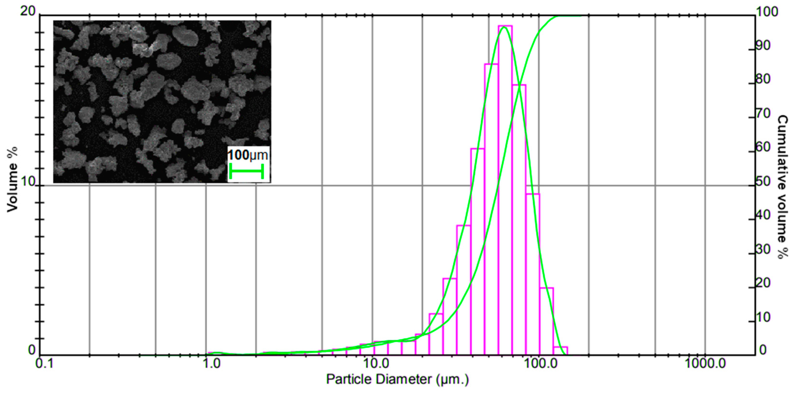
2.1. Materials
2.2. Conductive Composite Fabrication
2.3. Soldering Methods
2.4. Composite Surface Preparation Methods
3. Results and Discussion
3.1. Solder Wettability Test
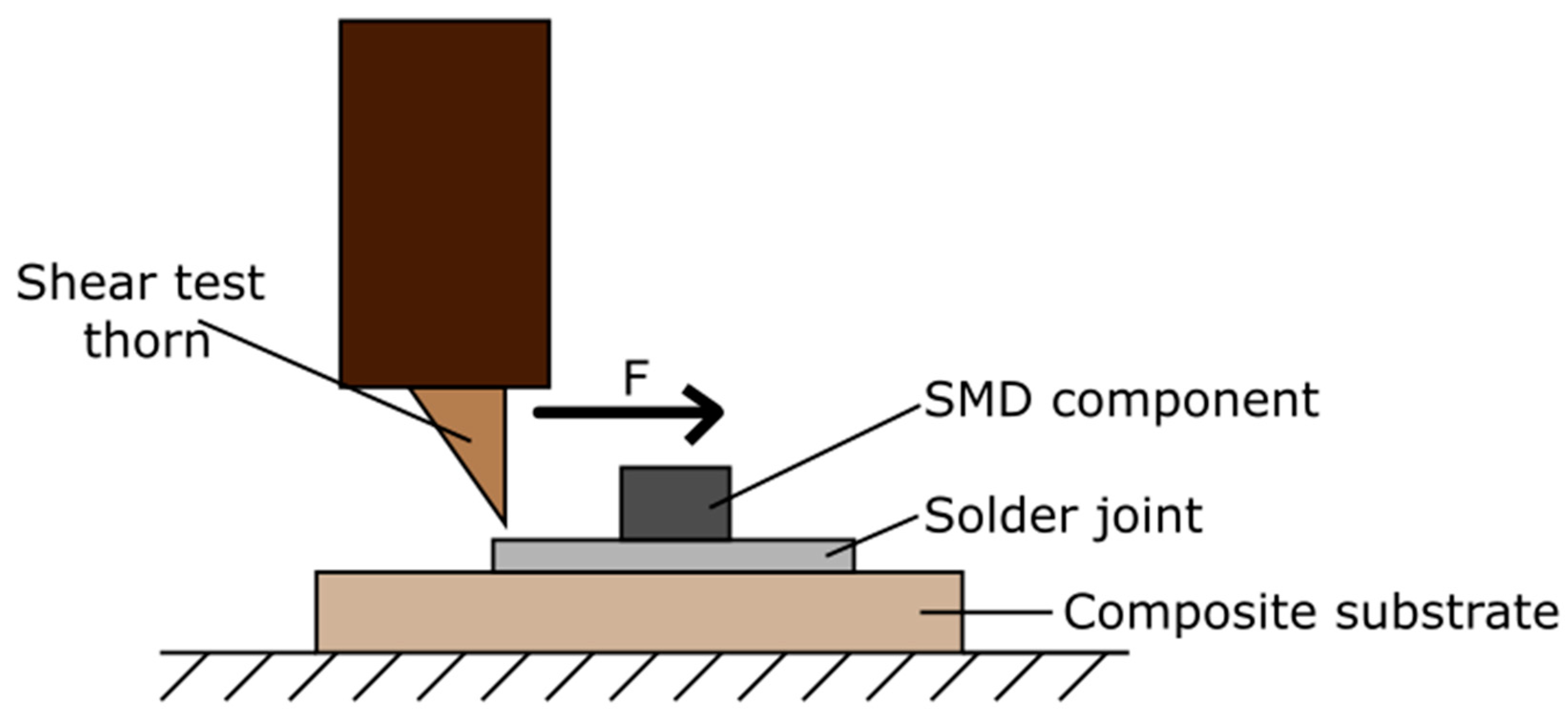
3.2. Shear Test
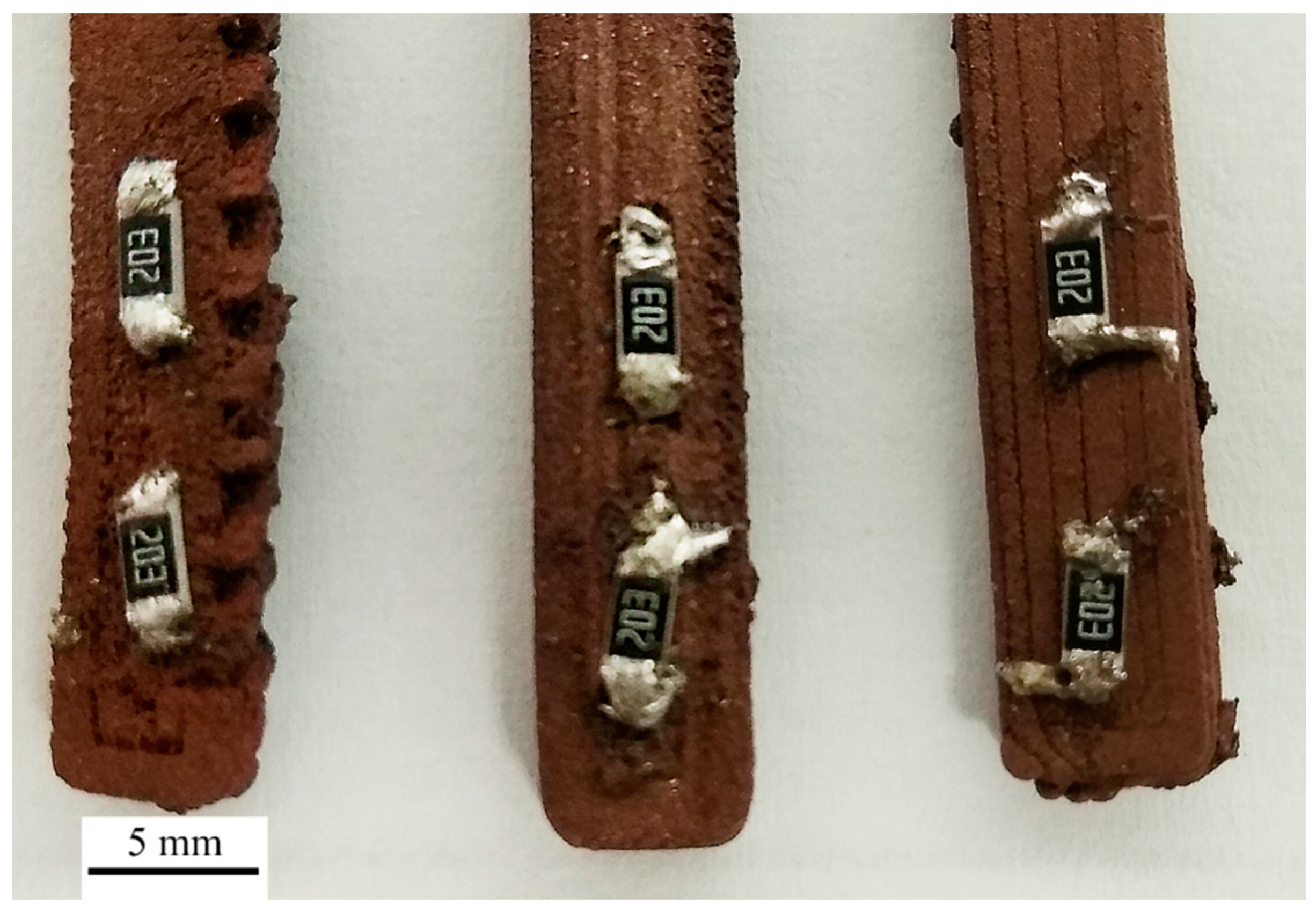
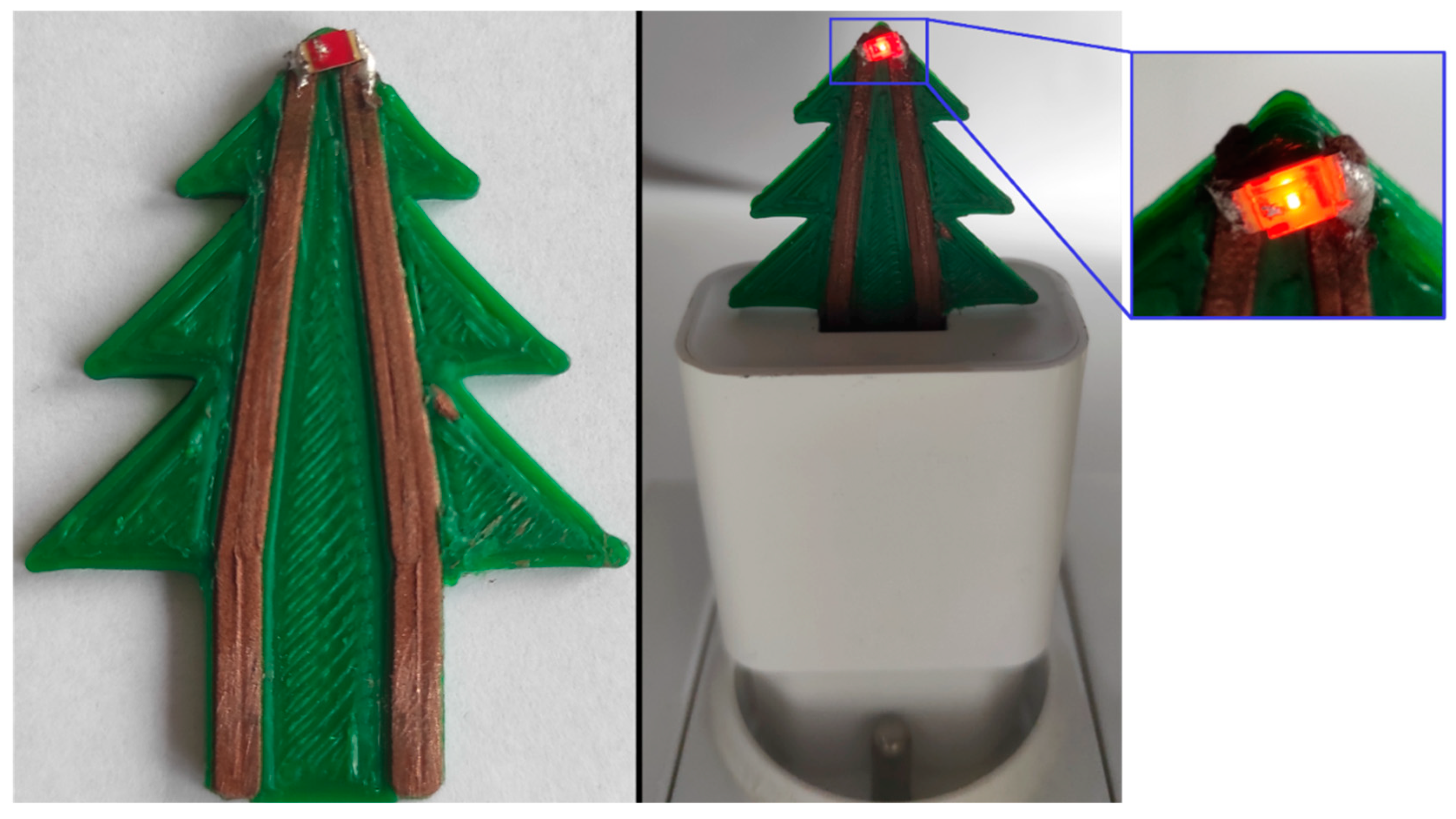
3.3. Demonstrator Fabrication
4. Conclusions
- The surface preparation of conductive composite plays a significant role in forming high-quality solder joints. The influence of surface preparation was evaluated by measuring the contact angle of the melted solder alloy. It can be observed that the best results were obtained with the mechanical removing of a thin polymer layer, revealing a copper powder inside a composite structure, and using flux that allows the removal of oxides and other compounds from the soldered surfaces. After the surface preparation, the contact angle value was reduced to 55° for reflow soldering with low-temperature SnBiAg solder paste, which fits the criteria of acceptable wetting.
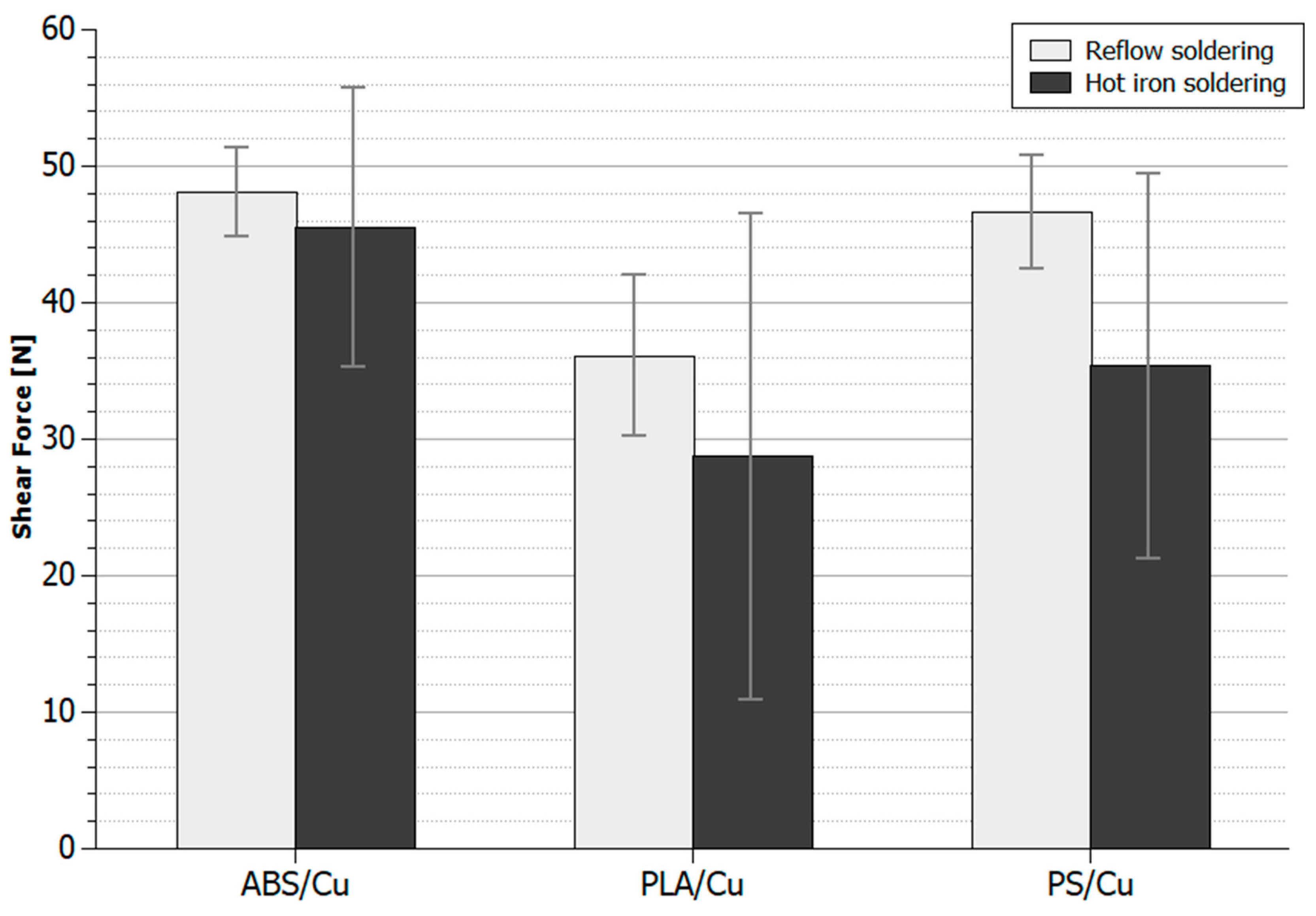
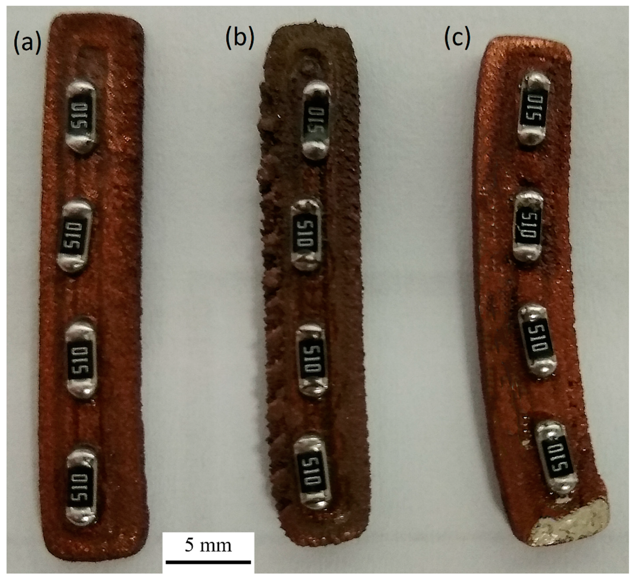
- The shear test results show that the maximum force value that could be applied before damaging soldered joints is strongly dependent on the polymer matrix used in the composite substrate. In general, maximum shear force values for reflow soldering are slightly higher than for hot iron soldering. Shear forces obtained for polymer composites as substrate are around 50% lower compared to a typical copper substrate.
- The highest average shear strength of the joint occurs on ABS/Cu substrates, then on PS/Cu, and the lowest results were obtained for the PLA/Cu substrate. The obtained results correlate directly with the thermal stability of the polymer matrixes used. The higher the thermal stability of the substrate material, the higher the maximum shear force of the soldered joints fabricated on that substrate.
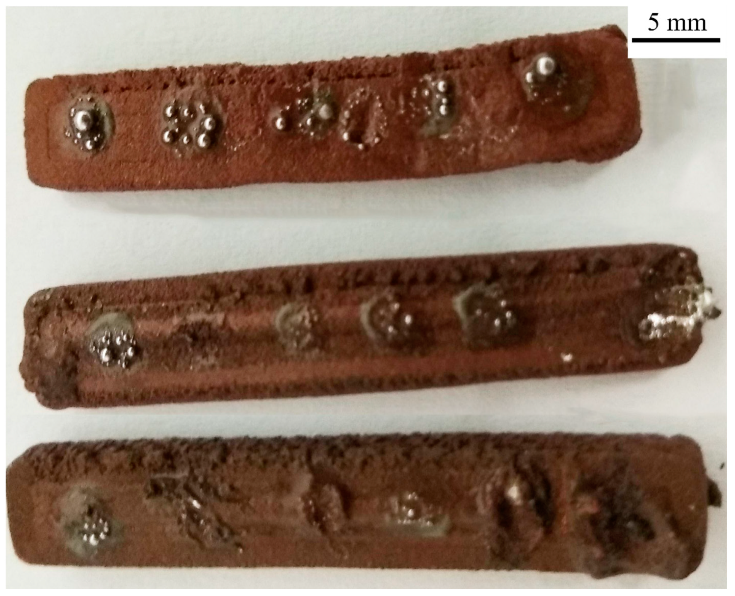
- Hot iron soldering can be used to fabricate soldered joints on prepared composite composites. Still, it is recommended that this method only be used for rapid prototyping of individual structures because of its low repeatability.
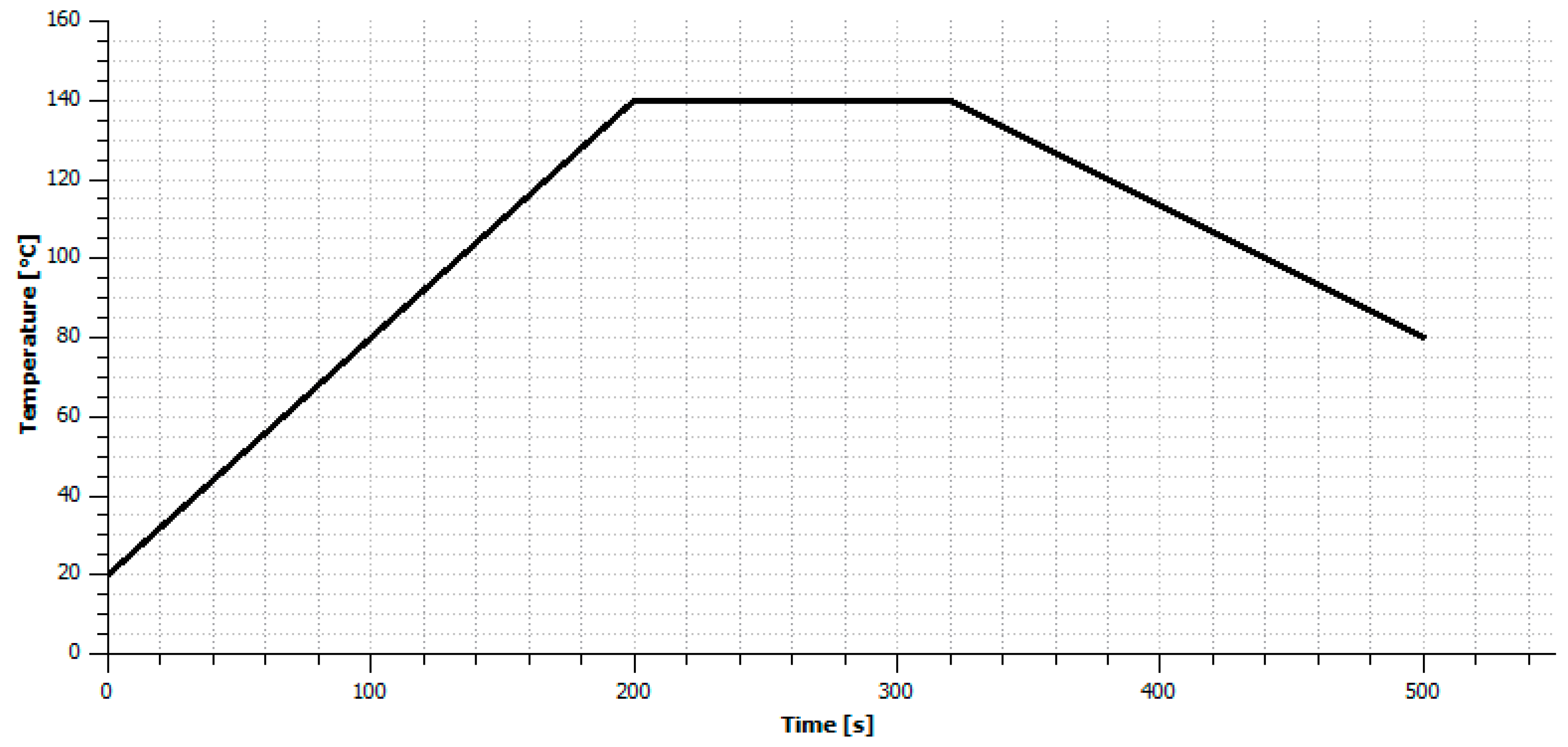
- The soldering joints with the best properties were obtained using low-temperature SnBiAg solder paste and reflow soldering. This allows the fabrication of repeatable, high-quality solder joints without damaging the composite substrate. This method can be used for the mass production of structural electronics elements.
Author Contributions
Funding
Institutional Review Board Statement
Informed Consent Statement
Data Availability Statement
Acknowledgments
Conflicts of Interest
References
- Conner, B.P.; Manogharan, G.P.; Martof, A.N.; Rodomsky, L.M.; Rodomsky, C.M.; Jordan, D.C.; Limperos, J.W. Making sense of 3-D printing: Creating a map of additive manufacturing products and services. Addit. Manuf. 2014, 1, 64–76. [Google Scholar] [CrossRef]
- Huang, Y.; Leu, M.C.; Mazumder, J.; Donmez, A. Additive Manufacturing: Current State, Future Potential, Gaps and Needs, and Recommendations. J. Manuf. Sci. Eng. 2015, 137, 014001. [Google Scholar] [CrossRef] [Green Version]
- Uriondo, A.; Esperon-Miguez, M.; Perinpanayagam, S. The present and future of additive manufacturing in the aerospace sector: A review of important aspects. Proc. Inst. Mech. Eng. Part G J. Aerosp. Eng. 2015, 229, 2132–2147. [Google Scholar] [CrossRef]
- Yap, Y.L.; Yeong, W. Additive manufacture of fashion and jewellery products: A mini review. Virtual Phys. Prototyp. 2014, 9, 195–201. [Google Scholar] [CrossRef]
- Yoshida, H.; Igarashi, T.; Obuchi, Y.; Takami, Y.; Sato, J.; Araki, M.; Miki, M.; Nagata, K.; Sakai, K.; Igarashi, S. Architecture-Scale Human-Assisted Additive Manufacturing. ACM Trans. Graph. 2015, 34, 88. [Google Scholar] [CrossRef]
- Ngo, T.D.; Kashani, A.; Imbalzano, G.; Nguyen, K.T.Q.; Hui, D. Additive Manufacturing (3D Printing): A Review of Materials, Methods, Applications and Challenges. Compos. Part B Eng. 2018, 143, 172–196. [Google Scholar] [CrossRef]
- Farahani, R.D.; Chizari, K.; Therriault, D. Three-dimensional printing of freeform helical microstructures: A review. Nanoscale 2014, 6, 10470–10485. [Google Scholar] [CrossRef] [PubMed]
- Ahn, B.Y.; Duoss, E.B.; Motala, M.J.; Guo, X.; Park, S.-I.; Xiong, Y.; Yoon, J.; Nuzzo, R.G.; Rogers, J.A.; Lewis, J.A. Omnidi-rectional Printing of Flexible, Stretchable, and Spanning Silver Microelectrodes. Science 2009, 323, 1590–1593. [Google Scholar] [CrossRef] [PubMed] [Green Version]
- Lewis, J.A.; Ahn, B.Y. Three-dimensional printed electronics. Nature 2015, 518, 42–43. [Google Scholar] [CrossRef] [PubMed]
- Maalderink, H.H.H.; Bruning, F.B.J.; De Schipper, M.M.R.; Van Der Werff, J.J.J.; Germs, W.W.C.; Remmers, J.J.C.; Meinders, E.R. 3D Printed structural electronics: Embedding and connecting electronic components into freeform electronic devices. Plast. Rubber Compos. 2017, 47, 35–41. [Google Scholar] [CrossRef]
- Lopes, A.J.; MacDonald, E.; Wicker, R.B. Integrating stereolithography and direct print technologies for 3D structural electronics fabrication. Rapid Prototyp. J. 2012, 18, 129–143. [Google Scholar] [CrossRef]
- MacDonald, E.; Salas, R.; Espalin, D.; Perez, M.; Aguilera, E.; Muse, D.; Wicker, R.B. 3D Printing for the Rapid Prototyping of Structural Electronics. IEEE Access 2014, 2, 234–242. [Google Scholar] [CrossRef]
- Espera, A.H.; Dizon, J.R.C.; Chen, Q.; Advincula, R.C. 3D-printing and advanced manufacturing for electronics. Prog. Addit. Manuf. 2019, 4, 245–267. [Google Scholar] [CrossRef]
- Dul, S.; Fambri, L.; Pegoretti, A. Fused deposition modelling with ABS–graphene nanocomposites. Compos. Part A Appl. Sci. Manuf. 2016, 85, 181–191. [Google Scholar] [CrossRef]
- Hwang, S.; Reyes, E.I.; Moon, K.-S.; Rumpf, R.C.; Kim, N.S. Thermo-mechanical Characterization of Metal/Polymer Composite Filaments and Printing Parameter Study for Fused Deposition Modeling in the 3D Printing Process. J. Electron. Mater. 2015, 44, 771–777. [Google Scholar] [CrossRef]
- Kuester, S.; Merlini, C.; Barra, G.M.; Ferreira, J.C.; Lucas, A.; de Souza, A.C.; Soares, B.G. Processing and characterization of conductive composites based on poly(styrene-b-ethylene-ran-butylene-b-styrene) (SEBS) and carbon additives: A comparative study of expanded graphite and carbon black. Compos. Part B Eng. 2016, 84, 236–247. [Google Scholar] [CrossRef]
- Ning, F.; Cong, W.; Qiu, J.; Wei, J.; Wang, S. Additive manufacturing of carbon fiber reinforced thermoplastic composites using fused deposition modeling. Compos. Part B Eng. 2015, 80, 369–378. [Google Scholar] [CrossRef]
- Ryder, M.A.; Lados, D.A.; Iannacchione, G.S.; Peterson, A.M. Fabrication and properties of novel polymer-metal composites using fused deposition modeling. Compos. Sci. Technol. 2018, 158, 43–50. [Google Scholar] [CrossRef]
- Hirman, M.; Steiner, F. A comparison of the shear strength of conductive adhesives and soldering alloys. In Proceedings of the 2015 38th International Spring Seminar on Electronics Technology (ISSE), Eger, Hungary, 6–10 May 2015; pp. 167–172. [Google Scholar]
- Jojibabu, P.; Jagannatham, M.; Haridoss, P.; Ram, G.J.; Deshpande, A.; Bakshi, S.R. Effect of different carbon nano-fillers on rheological properties and lap shear strength of epoxy adhesive joints. Compos. Part A Appl. Sci. Manuf. 2016, 82, 53–64. [Google Scholar] [CrossRef]
- Jeevi, G.; Nayak, S.K.; Kader, M.A. Review on adhesive joints and their application in hybrid composite structures. J. Adhes. Sci. Technol. 2019, 33, 1497–1520. [Google Scholar] [CrossRef]
- Ji, X.; Xiao, G.; Jin, T.; Shu, X. Shear properties of isotropic conductive adhesive joints under different loading rates. J. Adhes. 2018, 95, 204–217. [Google Scholar] [CrossRef]
- Sánchez-Romate, X.X.F.; Jiménez-Suárez, A.; Molinero, J.; Sánchez, M.; Güemes, A.; Ureña, A. Development of bonded joints using novel CNT doped adhesive films: Mechanical and electrical properties. Int. J. Adhes. Adhes. 2018, 86, 98–104. [Google Scholar] [CrossRef]
- Podsiadły, B.; Skalski, A.; Wałpuski, B.; Słoma, M. Heterophase Materials for Fused Filament Fabrication of Structural Elec-tronics. J. Mater Sci. Mater Electron. 2019, 30, 1236–1245. [Google Scholar] [CrossRef]
- Noor, E.E.M.; Singh, A.; Chuan, Y.T. A review: Influence of nano particles reinforced on solder alloy. Solder. Surf. Mt. Technol. 2013, 25, 229–241. [Google Scholar] [CrossRef]
- Jothi Prakash, C.G.; Prasanth, R. Approaches to Design a Surface with Tunable Wettability: A Review on Surface Properties. J. Mater. Sci. 2021, 56, 108–135. [Google Scholar] [CrossRef]
- Zhevnenko, S.N. Surface Free Energy of Copper-Based Solid Solutions. J. Phys. Chem. C 2015, 119, 2566–2571. [Google Scholar] [CrossRef]
- Vitos, L.; Ruban, A.; Skriver, H.; Kollár, J. The surface energy of metals. Surf. Sci. 1998, 411, 186–202. [Google Scholar] [CrossRef]
- Shimizu, R.N.; Demarquette, N.R. Evaluation of Surface Energy of Solid Polymers Using Different Models. J. Appl. Polym. Sci. 2000, 76, 1831–1845. [Google Scholar] [CrossRef]
- Wassink, R.J.K. Weichlöten in der Elektronik: Mit 303 Abb. u. 57 Tab. im Text; Leuze: Saulgau/Württ, Germany, 1986; ISBN 978-0-901150-14-1. [Google Scholar]
- Wedi, A.; Baither, D.; Schmitz, G. Contact angle and reactive wetting in the SnPb/Cu system. Scr. Mater. 2011, 64, 689–692. [Google Scholar] [CrossRef]
- Lin, C.-T.; Lin, K.-L. Contact angle of 63Sn–37Pb and Pb-free solder on Cu plating. Appl. Surf. Sci. 2003, 214, 243–258. [Google Scholar] [CrossRef]
- Garcia, L.R.; Osório, W.R.; Peixoto, L.C.; Garcia, A. Wetting Behavior and Mechanical Properties of Sn-Zn and Sn-Pb Solder Alloys. J. Electron. Mater. 2009, 38, 2405–2414. [Google Scholar] [CrossRef]
- Plevachuk, Y.; Hoyer, W.; Kaban, I.; Kohler, M.; Novakovic, R.; Plevachuk, Y. Experimental study of density, surface tension, and contact angle of Sn–Sb-based alloys for high temperature soldering. J. Mater. Sci. 2009, 45, 2051–2056. [Google Scholar] [CrossRef]
- Li, Y.; Wang, Z.; Li, X.; Lei, M. Effect of temperature and substrate surface roughness on wetting behavior and interfacial structure between Sn–35Bi–1Ag solder and Cu substrate. J. Mater. Sci. Mater. Electron. 2020, 31, 4224–4236. [Google Scholar] [CrossRef]
- Vianco, P.T.; Rejent, J.A.; Vianco, P.T.; Rejent, J.A. Properties of ternary Sn-Ag-Bi solder alloys: Part II—Wettability and mechanical properties analyses. J. Electron. Mater. 1999, 28, 1138–1143. [Google Scholar] [CrossRef]
- Fima, P.; Gąsior, W.; Sypien, A.; Moser, Z. Wetting of Cu by Bi–Ag based alloys with Sn and Zn additions. J. Mater. Sci. 2010, 45, 4339–4344. [Google Scholar] [CrossRef]
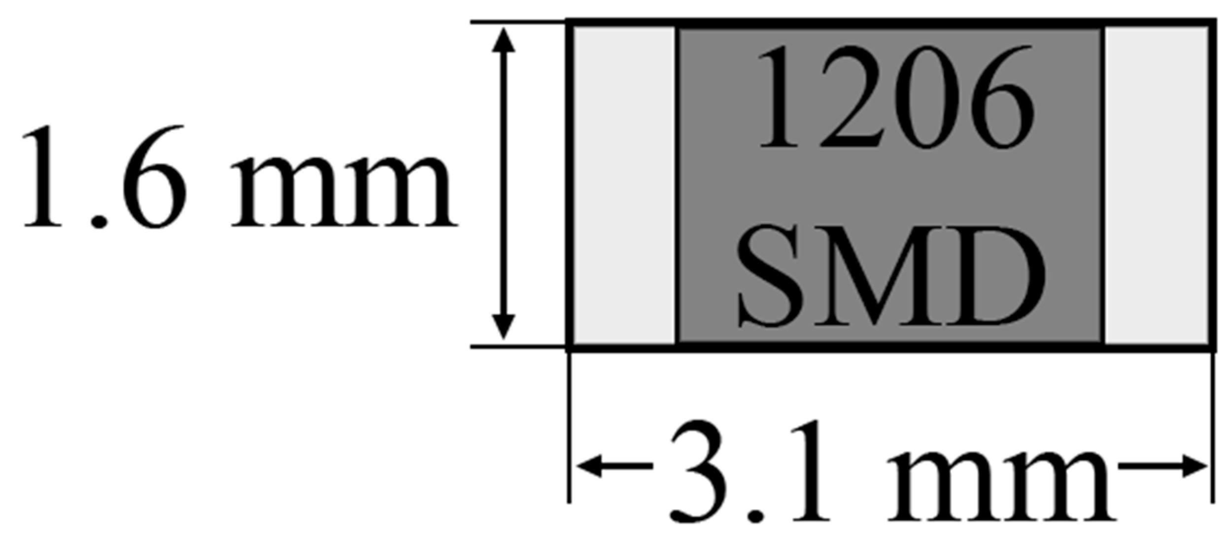
- Bernasko, P.K.; Mallik, S.; Takyi, G. Effect of intermetallic compound layer thickness on the shear strength of 1206 chip resistor solder joint. Solder. Surf. Mt. Technol. 2015, 27, 52–58. [Google Scholar] [CrossRef]
- Pan, J.; Toleno, B.J.; Chou, T.; Dee, W.J. The effect of reflow profile on SnPb and SnAgCu solder joint shear strength. Solder. Surf. Mt. Technol. 2006, 18, 48–56. [Google Scholar] [CrossRef]
- Espalin, D.; Muse, D.W.; MacDonald, E.; Wicker, R.B. 3D Printing Multifunctionality: Structures with Electronics. Int. J. Adv. Manuf. Technol. 2014, 72, 963–978. [Google Scholar] [CrossRef]


| Surface Section Symbol | A | B | C | D | E |
|---|---|---|---|---|---|
| A method of surface preparing | Surface mechanically cleaned with 400 grit sandpaper | RF800 flux applied on surface before soldering | Surface chemically cleaned with solvent | Surface mechanically cleaned with sandpaper and RF800 flux applied before soldering | No surface preparation before soldering |
| Surface Section Symbol | A | B | C | D | E |
|---|---|---|---|---|---|
| A Method of Surface Preparing | Surface mechanically cleaned with 400 grit sandpaper | RF800 flux applied on surface before soldering | Surface chemically cleaned with solvent | Surface mechanically cleaned with sandpaper and RF800 flux applied before soldering | No surface preparation before soldering |
| Solder Ball | 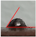 | 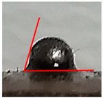 | 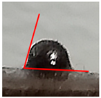 | 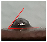 | 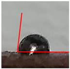 |
| EdgeDetection | 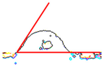 | 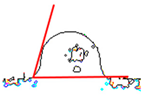 | 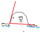 | 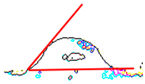 | 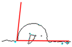 |
| Measured ContactAngle | 57° | 74° | 78° | 50° | 83° |
| Matrix Polymer | Surface Preparation Method | ||||
|---|---|---|---|---|---|
| A | B | C | D | E | |
| ABS | 57.82° ± 0.85° | 74.48° ± 0.82° | 78.07° ± 0.81° | 50.27° ± 0.95° | 83.74° ± 1.15° |
| PLA | 57.24° ± 0.85° | 74.09° ± 0.98° | 78.18° ± 0.79° | 50.48° ± 0.91° | 84.02° ± 1.19° |
| PS | 57.57° ± 1.11° | 74.34° ± 0.76° | 78.48° ± 0.77° | 50.55° ± 0.81° | 84.11° ± 1.18° |
| Solder Alloy | Soldering Method | Description | Fit the Criteria of Acceptable Wetting (θ < 55°) |
|---|---|---|---|
| SnPb | Hot iron soldering | Possible to fabricate soldered joints on all tested composite substrates; the method of surface preparation does not affect the quality of joints; not possible to determine the wetting angle; irregular shape of the obtained soldered joints | yes |
| SnPb | Reflow soldering | Not possible to fabricate soldered connections due to the high melting point of the soldering alloy (significantly exceeding the softening temperature of the polymer matrixes in all tested composites) | no |
| SnBiAg | Hot iron soldering | Not possible to fabricate solder joints due to the significant difference in wettability between the composite substrates and the soldering tip; soldering alloy sticks to the soldering tip and does not deposit on the composite substrate | no |
| SnBiAg | Reflow soldering | Possible to fabricate repeatable soldered joints; quality of soldered joints depends mainly on how the composite substrate’s surface is prepared; minor impact of the type of composite matrix on the quality of joints | yes |
| Polymer | Glass Transition Temperature (Tg) [°C] | Average Shear Force (Reflow Soldering) [N] | Average Shear Force (Hot Iron Soldering) [N] |
|---|---|---|---|
| ABS | 105 | 48.1 | 45.5 |
| PS | 100 | 46.7 | 35.4 |
| PLA | 60 | 36.1 | 28.7 |
Publisher’s Note: MDPI stays neutral with regard to jurisdictional claims in published maps and institutional affiliations. |
© 2021 by the authors. Licensee MDPI, Basel, Switzerland. This article is an open access article distributed under the terms and conditions of the Creative Commons Attribution (CC BY) license (https://creativecommons.org/licenses/by/4.0/).
Share and Cite
Podsiadły, B.; Skalski, A.; Słoma, M. Soldering of Electronics Components on 3D-Printed Conductive Substrates. Materials 2021, 14, 3850. https://doi.org/10.3390/ma14143850
Podsiadły B, Skalski A, Słoma M. Soldering of Electronics Components on 3D-Printed Conductive Substrates. Materials. 2021; 14(14):3850. https://doi.org/10.3390/ma14143850
Chicago/Turabian StylePodsiadły, Bartłomiej, Andrzej Skalski, and Marcin Słoma. 2021. "Soldering of Electronics Components on 3D-Printed Conductive Substrates" Materials 14, no. 14: 3850. https://doi.org/10.3390/ma14143850
APA StylePodsiadły, B., Skalski, A., & Słoma, M. (2021). Soldering of Electronics Components on 3D-Printed Conductive Substrates. Materials, 14(14), 3850. https://doi.org/10.3390/ma14143850