Article

Influence of Co-Sputtered Ag:Al Ultra-Thin Layers in Transparent V2O5/Ag:Al/AZO Hole-Selective Electrodes for Silicon Solar Cells

1
Departament de Física Aplicada, Universitat de Barcelona, 08028 Barcelona, Spain
2
Institute of Nanoscience and Nanotechnology (IN2UB), Universitat de Barcelona, 08028 Barcelona, Spain
3
Departament d’Enginyeria Electrònica, Universitat Politècnica de Catalunya, 08034 Barcelona, Spain
*
Authors to whom correspondence should be addressed.
Materials 2020, 13(21), 4905; https://doi.org/10.3390/ma13214905
Submission received: 15 September 2020 / Revised: 23 October 2020 / Accepted: 29 October 2020 / Published: 31 October 2020
(This article belongs to the Section Thin Films and Interfaces)

Abstract

:
As optoelectronic devices continue to improve, control over film thickness has become crucial, especially in applications that require ultra-thin films. A variety of undesired effects may arise depending on the specific growth mechanism of each material, for instance a percolation threshold thickness is present in Volmer-Webber growth of materials such as silver. In this paper, we explore the introduction of aluminum in silver films as a mechanism to grow ultrathin metallic films of high transparency and low sheet resistance, suitable for many optoelectronic applications. Furthermore, we implemented such ultra-thin metallic films in Dielectric/Metal/Dielectric (DMD) structures based on Aluminum-doped Zinc Oxide (AZO) as the dielectric with an ultra-thin silver aluminum (Ag:Al) metallic interlayer. The multilayer structures were deposited by magnetron sputtering, which offers an industrial advantage and superior reliability over thermally evaporated DMDs. Finally, we tested the optimized DMD structures as a front contact for n-type silicon solar cells by introducing a hole-selective vanadium pentoxide (V2O5) dielectric layer.

1. Introduction

The proliferation of photonic technologies seen in recent years has been enabled by a steadily increasing potential of the optoelectronic devices. Opening a new fan out of applications including sensing, anti-reflection coatings or energy harvesting devices among many others. Many of these applications employ pure metal and metal-containing films (e.g., Ag coated waveguides, V thin film optical switches etc. [1]). For those applications examples, the most important characteristics of the films are related to the film thickness, either directly dependent or indirectly. Therefore, it is very interesting to study an effective method to deposit atomically smooth ultra-thin metallic layers. Moreover, ultra-thin metallic layers are a very interesting alternative for their use in transparent conductive electrodes. Traditionally, these electrodes have been based on degenerate doped wide band gap semiconductors such as gallium-doped zinc oxide (GZO), fluorine-doped tin oxide (FTO) or tin-doped indium oxide (ITO) [2,3,4]. Transparent conducting oxides (TCOs) are widely used in research and industrial applications including LCD screens, touch panels, transparent electronics, or photovoltaic devices [5,6,7,8]. Particularly for photovoltaics, ITO is commonly used as the front transparent conductive electrode and plays a fundamental role in many types of solar cells, from conventional crystalline silicon solar cells to organic solar cells [9,10,11]. However due to its high-temperature processing, brittle nature, increasing cost due to the scarcity of indium and disadvantages in the terms of production [12,13], a continuous effort is being done in order to find suitable indium-free alternatives to ITO. Metallic nanowire networks, carbon nanotubes, conductive polymers, graphene, and ultra-thin metallic films [14,15,16,17,18] are some of the alternatives to potentially reduce the production cost in the photovoltaic (PV) industry. Recently, dielectric-metal-dielectric (DMD) structures have emerged as valid candidates to substitute the ITO electrode in silicon solar cells. DMD structures based on V2O5/Ag/V2O5, AZO/Ag/TiO2 have been previously studied and were fabricated using the thermal evaporation technique [19,20]. The main disadvantage of this method is the agglomeration of the metal, related to the particular growth mode (i.e., Volmer-Webber type) of the deposited film. Therefore, it becomes a necessity to deposit a seed (wetting) layer to avoid migration of metal atoms over the surface to form clusters [21,22]. The advantage of using a gold seed layer to avoid agglomeration in dopant-free Si solar cells using V2O5/Ag/V2O5 as selective contacts was demonstrated in [23]. Nevertheless, the deposition of a few nanometers gold seed layer by thermal evaporation could not easily scale up to industrial production.
Besides the great importance of the metallic layer in DMDs, choosing the proper dielectric is crucial for the final optoelectronic properties of the multi-layered stack. In this sense, transition metal oxides (TMOs) (e.g., vanadium, tungsten, and molybdenum oxides) are very interesting dielectrics for DMD structures. Some of the interesting features of TMOs are their refractive index, their large work function that ranges from 2 to 7 eV and their wide bandgap of more than 3 eV [24]. These materials possess an extraordinary transparency to visible light and can be used as the anti-reflective coating (ARC) on silicon due to their bandgap and refractive index. Furthermore, the deep work function allows TMOs to actively participate in the band structure of the device, selectively collecting holes over electrons.
Selective conductivity of holes and electrons is used to induce junctions or provide ohmic contacts with semiconductor materials (e.g., perovskite, c-Si or organic). Exploring and developing new hole and electron selective contacts has motivated increasingly active research in recent years. Particularly for crystalline silicon solar cells the interest has been due to the simple fabrication process and the rather high efficiencies obtained. Conventional crystalline silicon (c-Si) solar cells using the doped amorphous silicon (a-Si: H) as p and n layers have achieved a high record power conversion efficiency (PCE) of more than 25% [25,26]. Nevertheless, by choosing the appropriate materials for the charge transport layers (CTL) one can accomplish selective transport of one carrier while simultaneously blocking the other without the need for doping. Transition metal oxides have demonstrated excellent carrier selective properties as they work as hole-selective contacts for heterojunction silicon solar cells [27]. Among these, MoO3 as a hole-selective contact has obtained the highest PCE of more than 22% [28]. Other p-type materials such as graphene, CNTs and MXene also have shown an excellent hole-selective nature [29,30,31]. However, dopant-free heterojunction solar cells still need transparent conducting oxides to improve the series resistance of the device and the short-circuit current density (Jsc).
In this work the magnetron radiofrequency (RF) sputtering technique was used as a replacement of thermal evaporation to deposit DMDs. RF sputtering is an industrially suitable technique with excellent uniformity on large areas, high adhesion, purity, and high deposition rates [32,33,34]. Moreover, sputtering enables better control over thickness of the metallic layers [35,36] and may eliminate the more complex usage of a seed layer [37].
First, we developed a completely sputtered, cost-effective and stable DMD layer of AZO/Ag:Al/AZO and investigated its electrical and optical characteristics. To avoid clustering of the metal nanostructures in the ultra-thin films the Ag was co-sputtered with Al [38]. However, the AZO/Ag:Al/AZO layer does not promote a preferred hole-selectiveness. Later, it was accomplished by replacing the bottom AZO layer with a high-quality hole-selective V2O5 layer. Silicon solar cells were then fabricated using a front V2O5/Ag:Al/AZO multilayer electrode, which was optimized for the thickness of the V2O5.

2. Materials and Methods

For examining and optimizing the properties of the DMD AZO/Ag:Al/AZO multilayers these structures were deposited on Corning glass 1737F. Prior to deposition the substrate was cleaned using mild soap, deionized water and isopropanol and then dried using N2 gas. For the fabrication of solar cells, silicon substrate (n-type) was treated with hydrofluoric (HF) acid (1%) for 1 min before the deposition. All thin films were deposited by means of rf sputtering (ATC ORION 8 HV) using a 3-inch target. The vacuum chamber was pumped to a base pressure of 3 × 10⁻⁶ Torr prior to all the depositions. AZO films were deposited from ZnO:Al target (2 wt% of Al) of 99.99% purity. The depositions were done at different pressures in the range between 1 and 8 mTorr with a constant power of 150 W. Reactive argon hydrogen (Ar:H2) atmosphere (3.5% of H2) was maintained in the vacuum chamber. The films were deposited at room temperature and at 100 °C with a deposition rate of 3.5 nm/min. The ultra-thin sub-nanometer roughness Ag:Al metallic films were prepared by co-sputtering of Al and Ag at room temperature. The sputtering power of the Ag target (99.99% pure) was kept constant at 100 W whereas the power applied to Al target (99.99% pure) varied from 100 W to 175 W. The sputtering was performed in an atmosphere of argon and all the depositions were done at a base pressure of 1 mTorr. Thickness of the films was estimated from the deposition rates of 100 nm thick films of Al and Ag on glass at similar conditions. Thus, the Al content in the Ag:Al films can be estimated about 16% to 20% in different samples.
The DMD structures (AZO/Ag:Al/AZO) investigated in this work were fabricated by sandwiching ultra-thin Al:Ag films between two AZO layers. All the layers were grown by sputtering and thickness of the films was measured using both an Alpha-Step D-120 profilometer (Scientec, Les Ulis, France) and a SD 2100 ellipsometre (Plasmos, Munich, Germany). Sheet resistance (Rsh) of the films was measured using a four-point probe set-up (Jandel, Grand Union House, Leighton Buzzard UK). UV-Visible-NIR spectrophotometer Lambda 950 (Perkin Elmer, Shelton, CT, USA) was used to measure the optical transmittance of the films. The surface morphology and the percolation in the films were investigated by atomic force microscope (AFM) (Bruker Multimode 8 with Nanoscope, Santa Barbara, CA, USA), and SEM images (JEOL JSM-7001F, Tokyo, Japan). N-type (100) c-Si wafers with resistivity of 2 Ωcm, thickness of 280 µm, one-side polished, non-textured were used for the fabrication of solar cells. Four different solar cell architectures were developed with modifications in the hole-selective layer. One without sandwiching Ag:Al layer in AZO and V2O5, other three by incorporating Ag:Al layer with varied thickness of V2O5. Thermally evaporated V2O5 was used as the dopant-free hole-selective contact as reported in our previous work [23]. An intrinsic (i-type) a-Si:H and doped n-type a-Si:H layers were deposited on the rear side by plasma-enhanced chemical vapor deposition (PECVD) to provide a reference electron selective contact [39]. The lithographic patterning of 1 cm2 was defined as the active area and a 2-µm-thick Ag grid (4.5% shadow) was thermally evaporated as the front contact. Finally, the back-contact metallization was accomplished by thermally evaporating Al (1µm thick). A scheme of the prior explained device structure with varying parameters in the hole-selective layer are schematically described in Figure 1. Current density-voltage (J-V) characteristics of the fabricated solar cells were measured using a 94041A solar simulator (Newport, Irvine, CA, USA). External quantum efficiency (EQE) curves were measured using a QEX10 set-up (PV Measurements, Point Roberts, WA, USA).

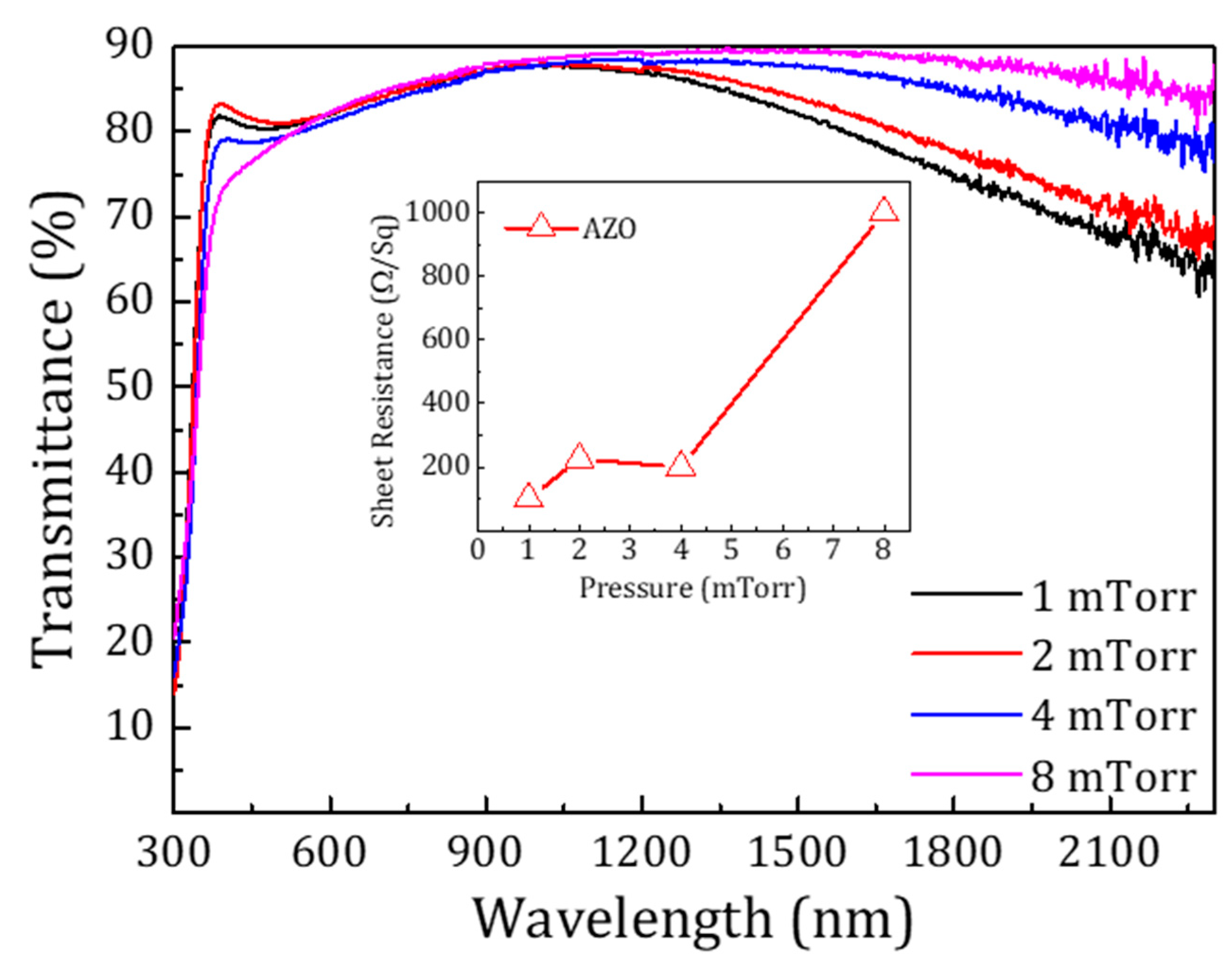
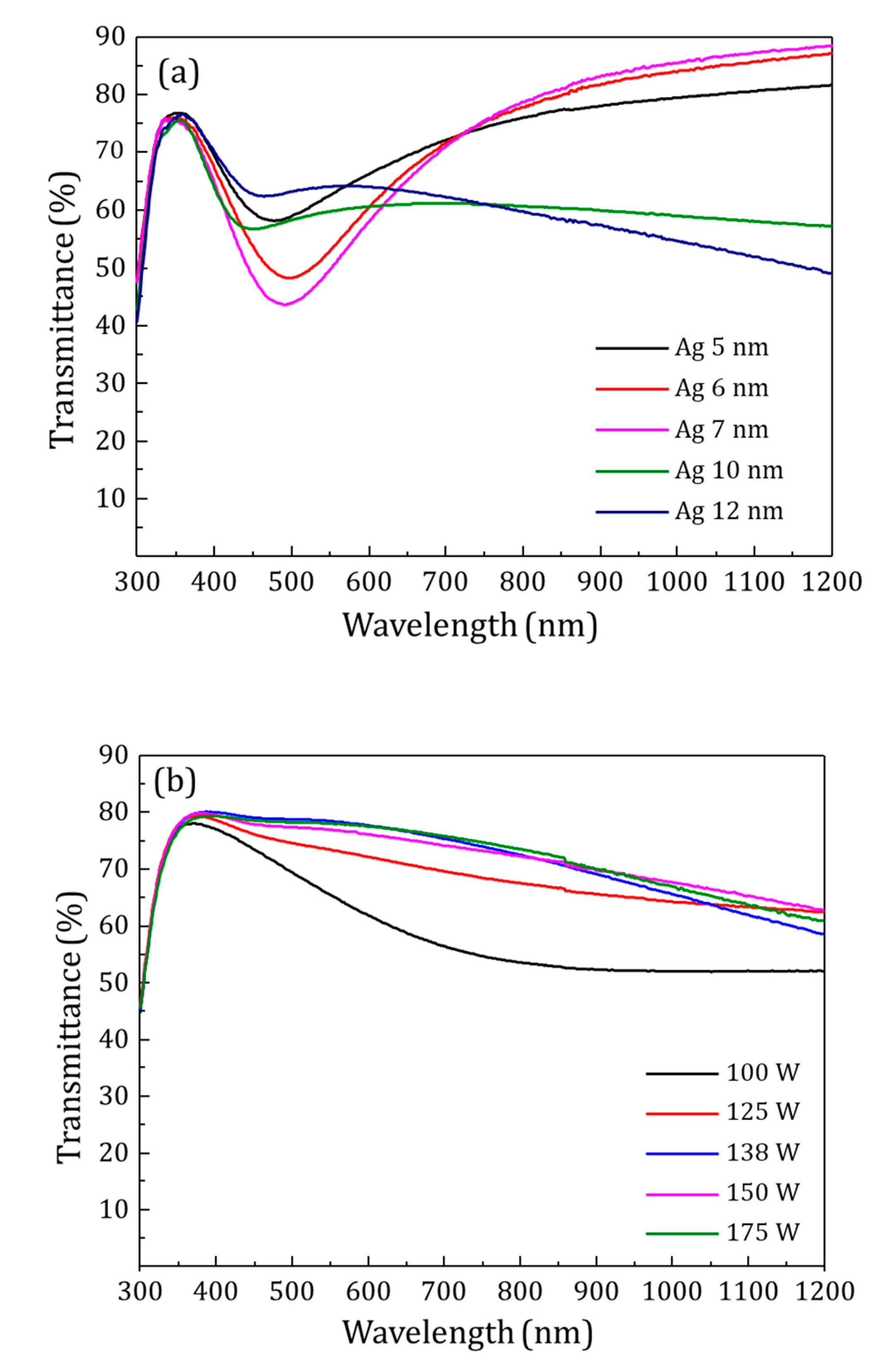
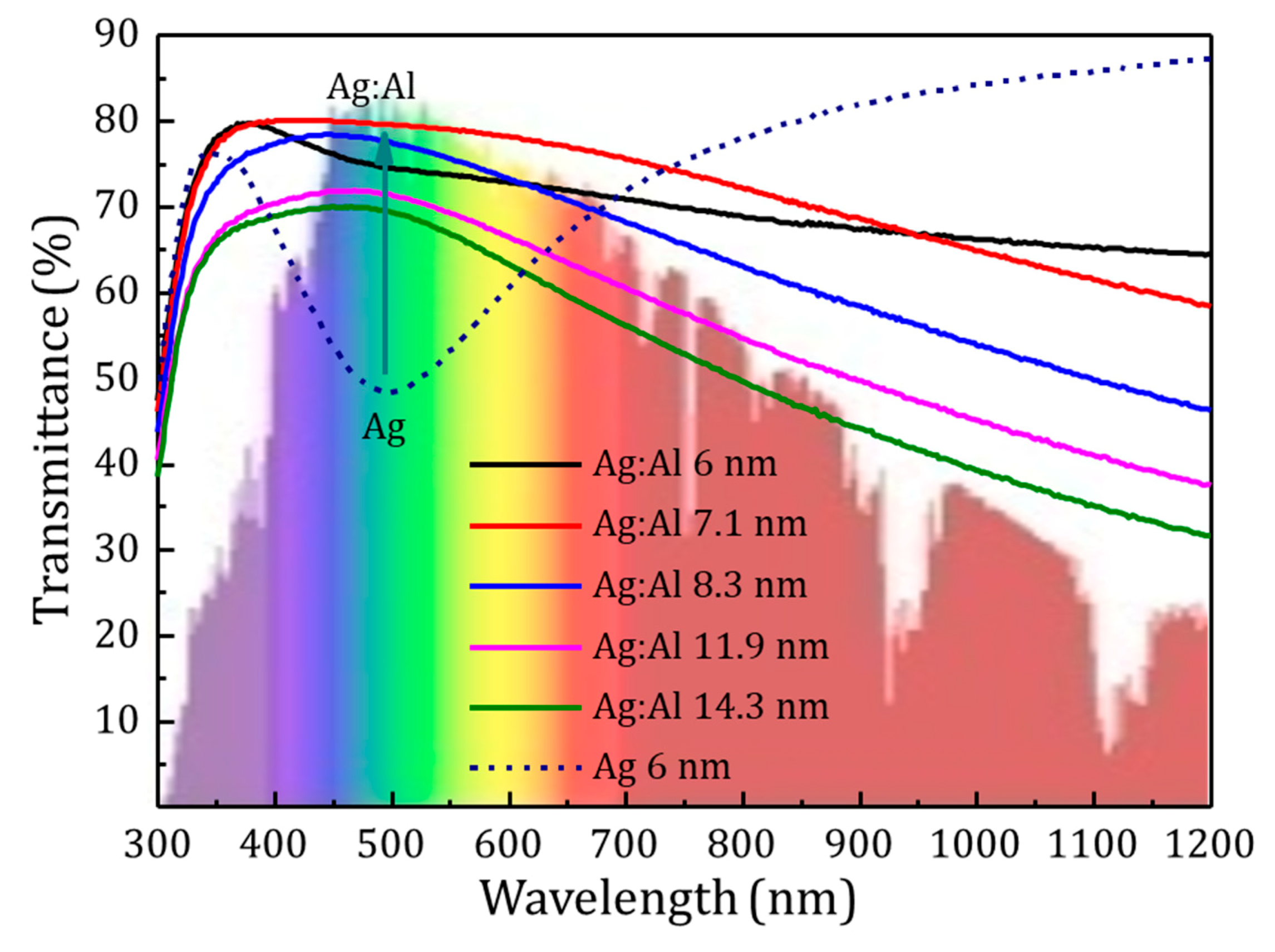
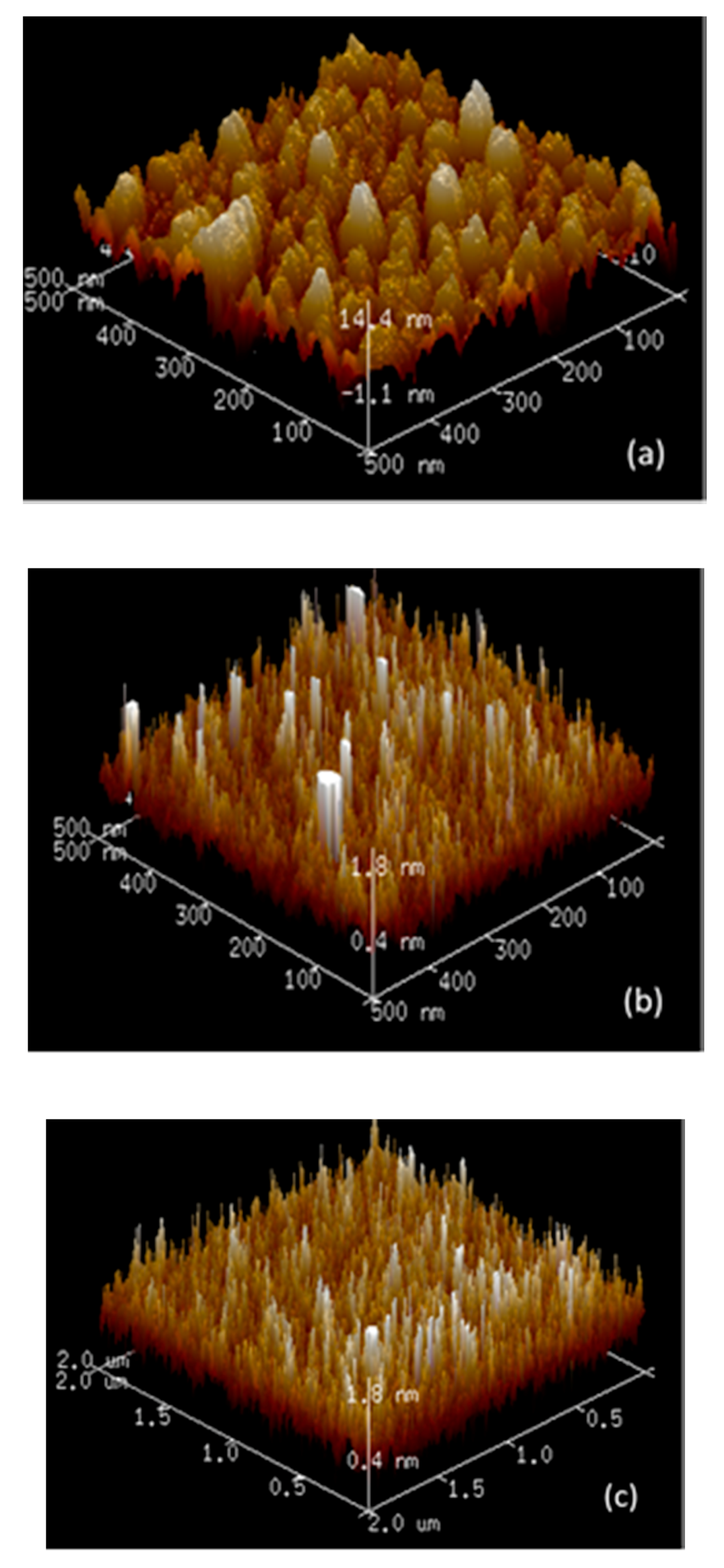
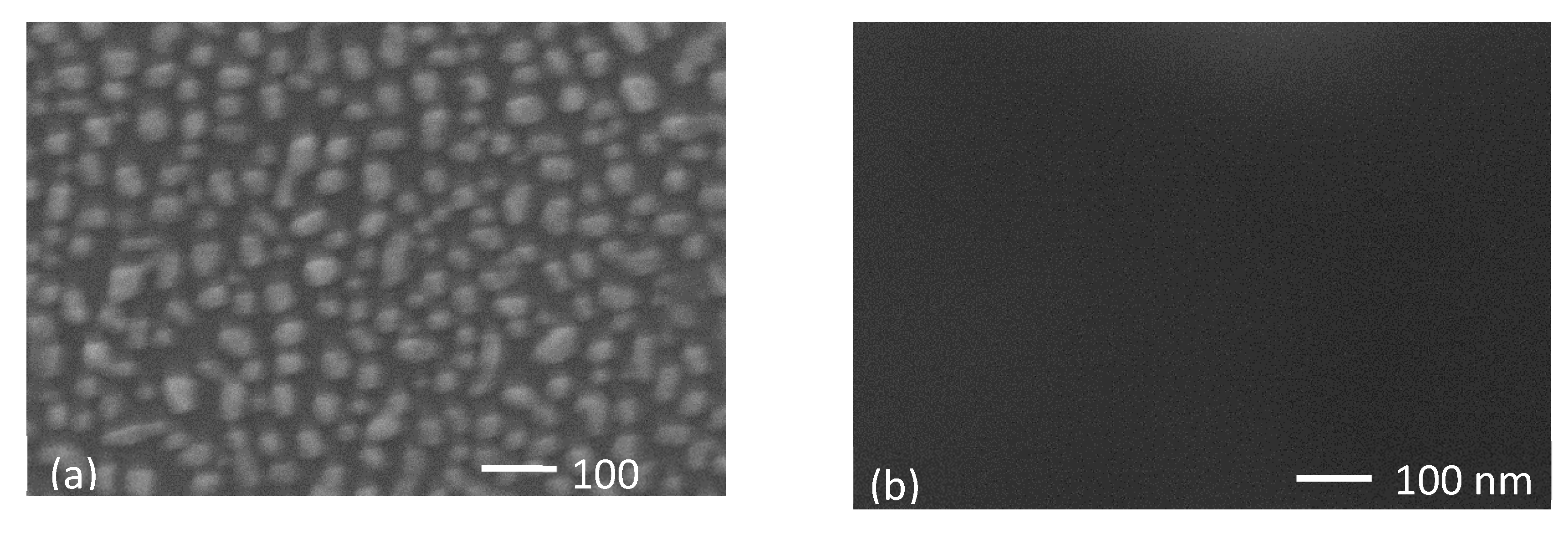
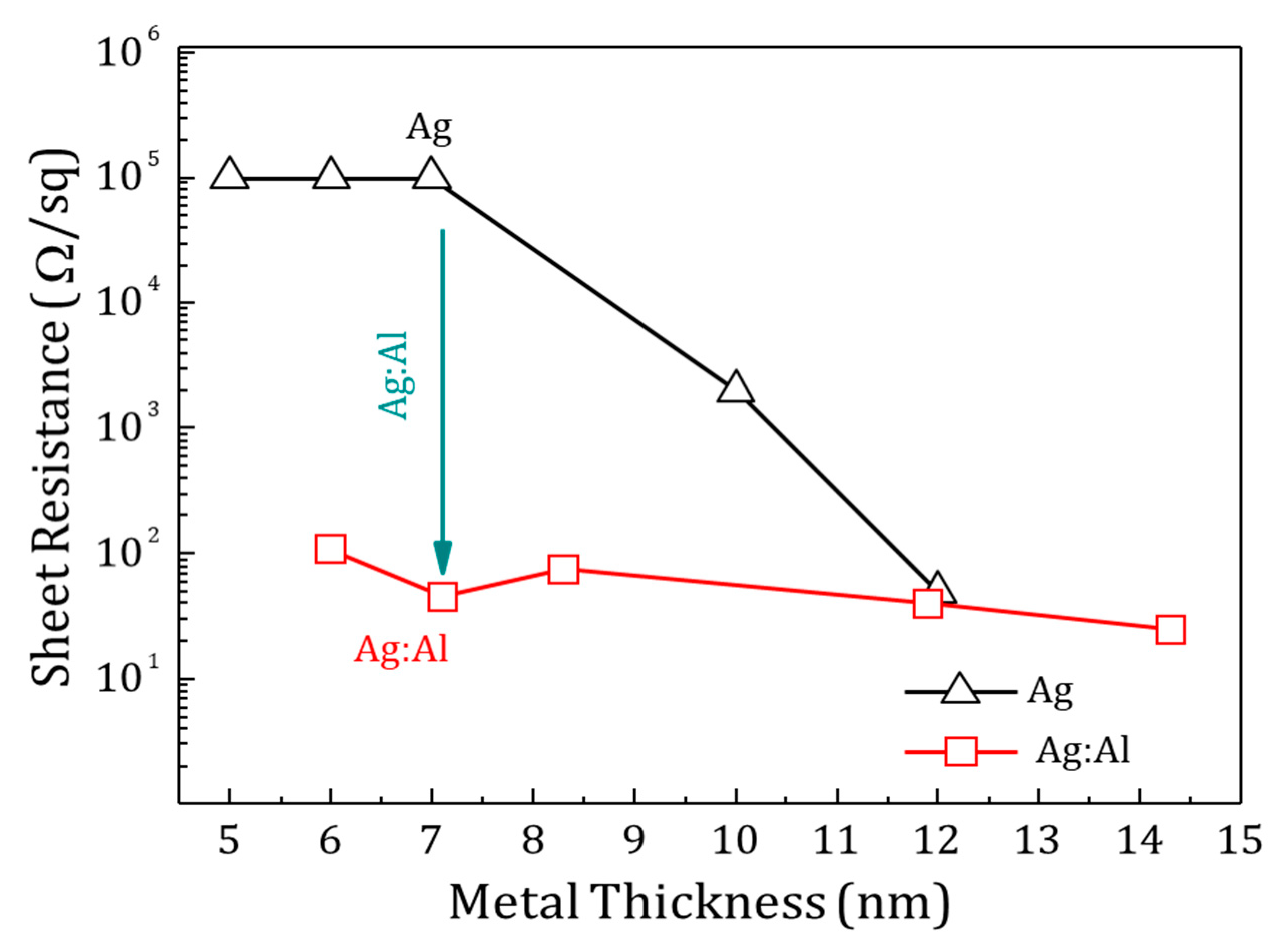
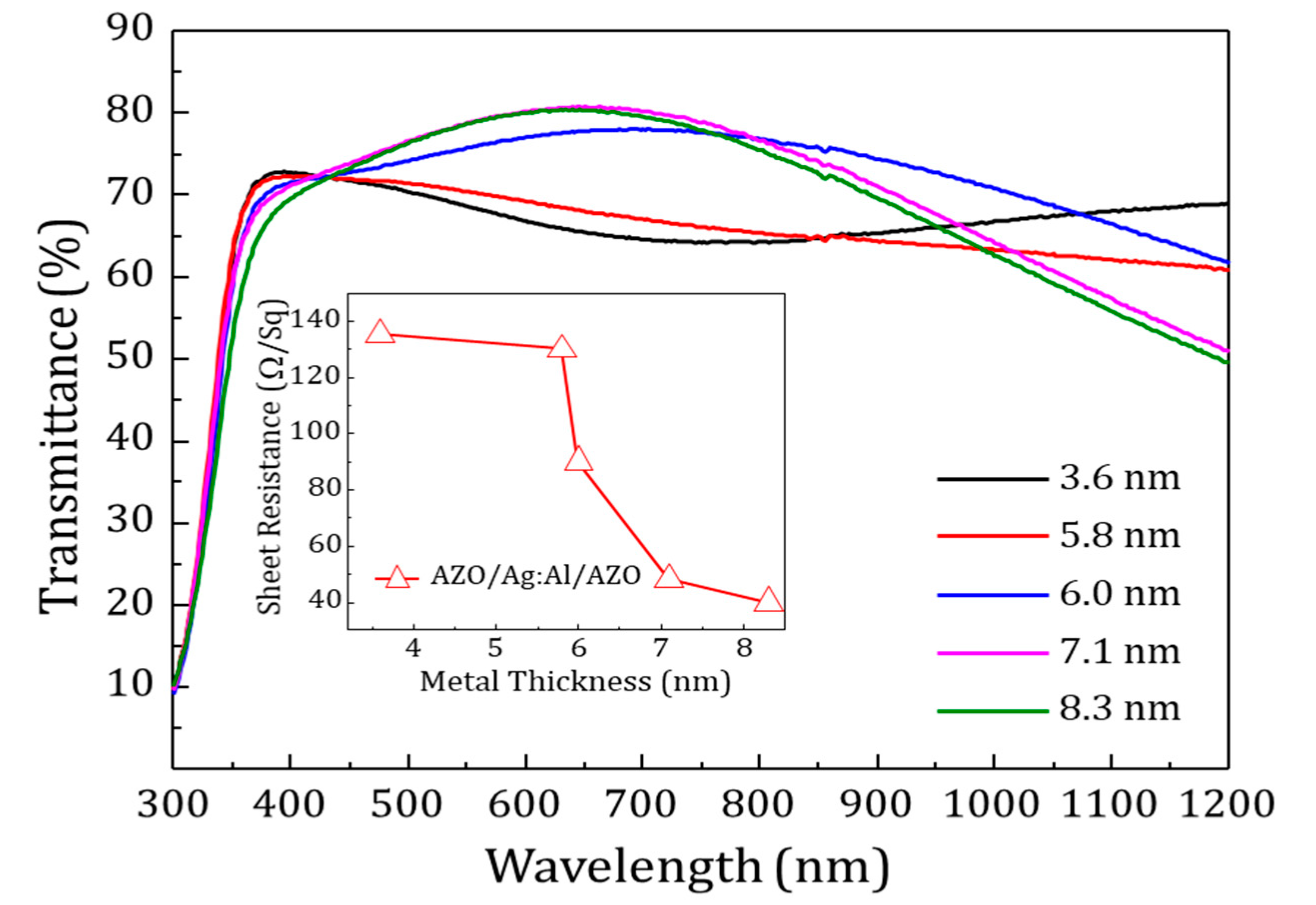
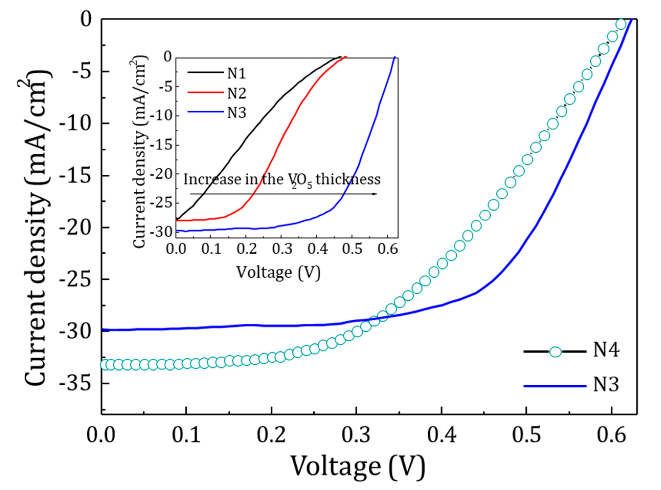
3. Results and Discussions

Electrical and optical characterization of the sputtered AZO films was carried out. The total thickness of all the films was kept around 75 nm that provides a good antireflection property [40,41].
Films were studied with varying pressure, keeping the temperature (100 °C) and power (150 W) as constant deposition parameters. A huge decrease in sheet resistance from kΩ/Sq to around 100 Ω/Sq was observed in the films by reducing the deposition pressure from 8 to 1 mTorr. This effect could be explained by the formation of oxygen vacancies or a higher hydrogen reduction of the films. This agrees with the steady decrease in the infrared transmittance of the films (see Figure 2) as the deposition pressure is reduced [42,43]. Transmittance measurements for the AZO films indicate that all the films grown at different pressures show an average transmittance of 80%. The transmittance of the films in the visible range was independent of the pressure as shown in Figure 2, whereas the inset shows the drop in sheet resistance as a function of the deposition pressure.
To improve the electric properties of the AZO films, an ultra-thin Ag film was sandwiched between two AZO layers. The optical properties and sheet resistance of this intermediate ultra-thin Ag films for thickness ranging from 5 to 12 nm were studied. Results showed that the broad drop in transmittance spectra within the visible region could be explained by the Volmer-Weber growth model [44], i.e., the tendency of silver nanoparticles to form islands during the first few nanometers (see Figure 3a). The absorption caused by the formation of localized surface plasmons would explain the comparatively low optical transmittance and electrical discontinuity [45,46]. Therefore, the pure Ag films were highly resistive, reaching sheet resistances greater than 105 Ω/Sq until a threshold thickness of 10 nm that leads to a sheet resistance of 2 × 10³ Ω/Sq.
To obtain ultra-smooth Ag-based films with reduced RMS roughness, electrical continuity and higher transmittance, Ag:Al films were prepared by co-sputtering of Al with Ag. Al doping enhances the density of heterogeneous nucleation sites, thus larger nuclear density and smaller particle size [38]. First, Ag:Al films were optimized for Al doping concentration with a constant power on Ag target. Figure 3b shows the transmittance of films deposited at varying powers of Al from 100 W to 175 W keeping constant the power of Ag 100 W. The higher transmittance and lower sheet resistance were obtained for the Ag:Al films sputtered at 138 W, with a transmittance of 75–80% in the visible region and a sheet resistance of 60 Ω/Sq. All other films showed higher sheet resistance.
Then several Ag:Al films with varying thickness co-sputtered with Al at 138 W have been studied. Figure 4 shows the comparison of optical transmittance of the pure Ag film of 6 nm layer and Ag:Al films with thickness ranging from 6 nm to 14 nm.
For the same thickness of Ag and Ag:Al samples, an increase of 30% transmittance was obtained for the later in the visible region. Thus, aiding to compensate for the broad dip in the transmittance spectra in ultra-thin Ag films. The atomic force microscope (AFM) images of the surface morphology of a 7 nm pure Ag film and 8.3 nm and 7.1 nm Ag:Al films are shown in Figure 5. The peak-to-valley height of pure Ag films with a maximum value of 14.4 nm and Ag:Al films with 1.8 nm exhibits the smoothness of the films. The RMS roughness value obtained for pure Ag film of 7 nm was 3.99 nm and for Ag:Al films with thicknesses 8.3 nm and 7.1 nm were 0.47 nm and 0.37 nm respectively. This lower RMS value confirms the ultra-smooth nature of the films. Figure 6 shows the SEM micrographs of the above-mentioned samples, which confirms the continuity in the films. The clustering of pure Ag films and the homogeneity in the Ag:Al films were easily observable.
Grazing incidence X-ray diffraction analysis evidenced some crystalline microstructure for the Ag:Al film observed in Figure 6b, which is quite remarkable for such an ultrathin film (i.e., 7.1 nm). On the other hand, the V2O5 layer was completely amorphous and the AZO layer evidenced an oriented pattern compatible with ZnO-Hexagonal phase.
Sheet resistance with the increasing thickness of Ag and Ag:Al films are shown in Figure 7. The Ag films with thickness less than 7 nm behave as insulators with a high sheet resistance of 105 Ω/Sq. Ag:Al films of similar thickness show a sheet resistance of several 100 Ω/Sq. The huge drop in sheet resistance in Ag:Al films was due to the enhanced density of heterogeneous nucleation sites, avoiding the formation of isolated islands in the films [45]. The calculated resistivity of the Ag:Al films was comparable to the bulk resistivity of Ag films, confirming the uniform nature of the films.
The influence of the Ag:Al layers on the AZO/Ag:Al/AZO structures was investigated by studying the electrical and optical properties of the multilayers. Figure 8 shows the transmittance spectra for various metal thicknesses and the inset displays the sheet resistance as a function of metal thickness for AZO/Ag:Al/AZO multilayer.
The thickness of the AZO layers was fixed as 18 nm and 70 nm for the bottom and top layer respectively. The optimized Ag:Al films sputtered at 138 W with varying thickness from 3 to 8.1 nm were used for the study. As the thickness of the intermediate layer increased, a decrease in sheet resistance and an increase in transmittance was observed in the multilayer structure. The intermediate layer of 7.1 nm showed the best result with a lower sheet resistance of 48 Ω/Sq and higher transmittance of 80% in the visible region.
Considering the final step to fabricate TCO for devices, figure of merit (FOM) values were calculated for these structures. The FOM defined by Haacke, ФTC = T10/Rs [47], was calculated in the range 400–800 nm for ITO, AZO thin film and multi-layered structure, and the values are given in Table 1. The FOMs were estimated for reduced AZO films (Ar:H2 atmosphere) at 100 °C and at room temperature (RT) and for non-reduced AZO films (Ar atmosphere) at RT. The multilayer structure attained the highest FOM of 1.9 × 10⁻³−1 compared to other films, which layed between 2 × 10⁻⁵−1 and 1.1 × 10⁻³−1. The FOM values achieved here are comparable to state of art TCOs used as antireflection coating in Si heterojunction solar cells, as reported by M.Nisha et al. [4]. This shows the potential of AZO/Ag:Al/AZO multilayer to replace ITO, which could be used as transparent conducting film in various optoelectronic devices such as large-area solar cells, diodes, photodetectors etc.
A carrier selective layer must be included to implement this electrode in photovoltaic devices. Thus, later studies were conducted to replace the AZO bottom layer with V2O5, to develop an all-in-one selective contact plus a transparent electrode for silicon-based solar cells. The V2O5 layer is needed to act as a dopant-free hole-selective layer. Even if they have clearly different electronic properties, replacing AZO by V2O5 as the bottom layer does not change much the transparency of the stack. The transfer-matrix method (TMM) algorithm developed in our previous work was used to predict the behavior of multilayer thin film structures [23]. The TMM algorithm for V2O5/Ag:Al/AZO multilayers predicted the optical performance of these structures on c-Si and, by integrating the air-mass 1.5 global irradiance (AM 1.5), the total photogenerated current Jph was calculated. Figure 9 shows the expected mapping of the current density for varying thickness of V2O5 and AZO with a fixed thickness of Ag:Al intermediate layer of 7.1 nm. From the simulation the optimum thickness for the finest optical properties and high photogenerated current for the AZO layer was between 40 and 80 nm. As far as the optimum thickness for V2O5 layer is concerned, the best performance could be expected below 20 nm or above 70 nm. However, we have some additional constraints for the implementation in the solar cell device. First, the thickness of the V2O5 layer should not be less than 20 nm to prevent damage at the interface during the sputtering step. On the other hand, it cannot be too thick, such as 100 nm, because of its insulating nature. The same calculation considering the whole AZO/Ag:Al/AZO stack deposited on the V2O5 selective layer predicted a reduction in the photogenerated current of about 2–3%. Thus, a direct V2O5/Ag:Al/AZO stack on silicon was preferred for device testing. The solar cells were fabricated with a fixed thickness of AZO layer at 50 nm, and different thicknesses of V2O5 layer from 20 to 50 nm.
As for the primary study the above conclusions were used, four different solar cell architectures (i.e., N1, N2, N3 and N4) were fabricated using different thicknesses for the V2O5 layer (25 nm, 35 nm, 50 nm and 50 nm respectively) as the hole-selective contact. Out of these, for N1, N2 and N3 cells V2O5/Ag:Al/AZO multilayer acted as hole transport and transparent conducting layer, while in N4 cell structure it was AZO/ V2O5 multilayer, i.e., without the metallic layer Ag:Al. For these studies the thickness of the AZO and Ag:Al layer was kept constant at 50 nm and 7.1 nm respectively. The thickness of the layers was chosen from the electrical, optical, and topographical aforementioned studies on the films of AZO and Ag:Al.
The J-V curves of devices N1, N2 and N3 showed that as the thickness of the V2O5 layer increased, there was a huge increase in the Voc from 459 mV to 631 mV and in the fill factor (FF) from 22 to 61% (inset of Figure 10). This variation could be explained by the formation of defects in the V2O5 layer during sputtering because of Ag and Al ion bombardment. As the thickness of the V2O5 layer increases the damaging effect decreases and the inversion layer made by V2O5 becomes sufficient to improve the Voc and other parameters of the cell. N4 device was fabricated with 50 nm thickness of the V2O5 layer, hence reducing the bombardment defects and improving the optical parameters. This device without the Ag:Al metallic layer shows a Voc = 614 mV, Jsc = 33.1 mA, FF = 47.5% and an efficiency η = 9.6% (Figure 10). The device N3 with same thickness of V2O5, shows Voc = 631 mV, Jsc = 29.8 mA, FF = 61.2% and η = 11.5%. These increases in Voc, FF and η in the device N3 could be directly attributed to the presence of the metallic Ag:Al layer which decreased the sheet resistance. All devices were measured under a simulated AM 1.5 irradiance of 100 mW/cm2. The photovoltaic parameters of all the cells are given in Table 2.
External quantum efficiency (EQE) of the solar cell with its reflectance spectrum are plotted in Figure 11. The EQE dropped at long wavelengths photon energies lower than the Si bandgap (λ > 1100 nm). On the other hand, at short wavelengths (λ < 500 nm) the EQE was reduced because of the absorption in the front layers (DMD) and recombination at the front interface. A balance of the current entities calculated by integrating the solar spectrum is computed in the inset, taking into account optical and internal recombination losses.
The maximum photocurrent that could be obtained for photon energies higher than the Si bandgap of 1.1 eV was 42.3 mA/cm2. Reflectance losses of 11.3% on the front surface of the cell reduced the photogenerated current to 37.5 mA/cm2. The final photogenerated current value limits to 29.8 mA/cm2 due to the internal loss of 20.6% in the solar cell. Photocurrent losses in the c-Si bulk and the rear contact were expected to be very low accounting for the high-quality substrate and rear surface passivated contact. Thus, the 20.6% internal photocurrent loss could be explained by the parasitic absorption in the vanadium oxide layer and mainly to the absorption in the Ag:Al metallic layer. The degradation of V2O5 during sputtering also increased the internal recombination that eventually led to a reduction in the Jsc value. Further optimization in the thickness of the vanadium oxide layer in the V2O5/Ag:Al/AZO stack could reduce the damage during the sputtering. The fabrication of solar cells on textured wafers assuming the same internal losses could also increase the Jsc value up to 2–3 mA/cm2. Finally, controlling the thickness of Ag:Al and AZO layers could lead to further improvement in the photogenerated Jsc value.

4. Conclusions

An all-in-one excellent transparent conductor and hole-selective contact layer V2O5/Ag:Al/AZO was developed. This substitutes for traditional TCOs and henceforth reduces the need for more expensive standard ITO electrodes. Moreover, the deposition employed magnetron sputtering method, which is more industrial than the thermal evaporation technique. At first, the successful TCO substitute was achieved through the fabrication and optimization of ultra-thin Ag:Al layer as an intermediate layer for the AZO-based DMD structure AZO/Ag:Al/AZO. Al doping in Ag layer helped to obtain ultra-thin smooth metallic films of higher transmittance and lower sheet resistance. The optimized AZO/Ag:Al/AZO multilayer structure showed a sheet resistance of 48 Ω/Sq and 80% transmittance in the visible region of the spectra.
Then, in order to develop a hole-selective layer for the fabrication of solar cells the above TCO multi-structure was reconfigured, i.e., by replacing the bottom AZO layer by V2O5. Hence forming a dopant-free V2O5/Ag:Al/AZO all-in-one TCO and hole-selective contact. Afterwards, solar cells were fabricated using this multilayer with varied thicknesses of the bottom V2O5 layer. The solar cell on n-type c-Si with 50 nm thickness of V2O5 yielded a PCE of 11.5% with remarkably high Voc of 631 mV and Jsc of 29.8 mA/cm2 showing its potential as an excellent TCO and as a hole-selective contact. The lower fill factor of 61.2% points out room for improvement in the contact by further optimization in the thickness of V2O5. Although we analyzed the potential of these structures on heterojunction solar cells, the concept could be applied to many other optoelectronic devices.

Author Contributions

Conceptualization, T.T. and E.R.; methodology, T.T., E.R. and C.V.; validation, C.V., J.M.A., and J.B.; formal analysis, T.T., J.B. and E.R.; investigation, T.T., E.R., C.V. and J.P.; data curation T.T., E.R., and N.L.-P.; writing—original draft, T.T.; software, E.R., N.L.-P. and J.M.A.; writing—review and editing; J.B., C.V., E.R. and J.A.; resources, J.B., C.V., J.P. and J.A.; supervision, J.B., J.P., J.M.A., C.V. and J.A.; funding acquisition, J.B., J.A., J.M.A. and C.V. All authors have read and agreed to the published version of the manuscript.

Funding

This research has been supported by the Spanish Ministerio de Economía, Industria y Competitividad and the European Regional Development Fund through the projects ENE2016-78933-C4-1-R, ENE2016-78933-C4-2-R, PID2019-109215RB-C41, PID2019-1092215RB-C43 and ENE2017-87671-C3-2-R. We acknowledge support of Secretaria d’Universitats i Recerca de la Generalitat de Catalunya and European Social Fund (2019 FI_B 00456).

Conflicts of Interest

The authors declare no conflict of interest.

References

  1. Whiteside, P.J.D.; Chininis, J.A.; Hunt, H.K. Techniques and challenges for characterizing metal thin films with applications in photonics. Coatings 2016, 6, 35. [Google Scholar] [CrossRef] [Green Version]
  2. Ponja, S.D.; Sathasivam, S.; Parkin, I.P.; Carmalt, C.J. Highly conductive and transparent gallium doped zinc oxide thin films via chemical vapor deposition. Sci. Rep. 2020, 10, 1–7. [Google Scholar] [CrossRef] [PubMed] [Green Version]
  3. Swallow, J.E.N.; Williamson, B.A.D.; Whittles, T.J.; Birkett, M.; Featherstone, T.J.; Peng, N.; Abbott, A.; Farnworth, M.; Cheetham, K.J.; Warren, P.; et al. Self-compensation in transparent conducting F-doped SnO2. Adv. Funct. Mater. 2018, 28, 1–10. [Google Scholar] [CrossRef] [Green Version]
  4. Nisha, M.; Anusha, S.; Antony, A.; Manoj, R.; Jayaraj, M.K. Effect of substrate temperature on the growth of ITO thin films. Appl. Surf. Sci. 2005, 252, 1430–1435. [Google Scholar] [CrossRef]
  5. Batmunkh, M.; Dadkhah, M.; Shearer, C.J.; Biggs, M.J.; Shapter, J.G. Incorporation of graphene into SnO2 photoanodes for dye-sensitized solar cells. Appl. Surf. Sci. 2016, 387, 690–697. [Google Scholar] [CrossRef] [Green Version]
  6. Wu, C.C. Highly flexible touch screen panel fabricated with silver-inserted transparent ITO triple-layer structures. RSC Adv. 2018, 8, 11862–11870. [Google Scholar] [CrossRef] [Green Version]
  7. Lewis, B.G.; Paine, D.C. Applications and processing of transparent. MRS Bull. 2000, 25, 22–27. [Google Scholar] [CrossRef]
  8. Spooner, K.B.; Ganose, A.M.; Scanlon, D.O. Assessing the limitations of transparent conducting oxides as thermoelectrics. J. Mater. Chem. A 2020. [Google Scholar] [CrossRef] [Green Version]
  9. Luque, A.; Hegedus, S. Handbook of Photovoltaic Science and Engineering, 2nd ed.; John Wiley & Sons, Ltd.: Hoboken, NJ, USA, 2011. [Google Scholar]
  10. Moss, R.L.; Tzimas, E.; Kara, H.; Willis, P.; Kooroshy, J. Critical Metals in Strategic Energy Technologies; Publications Office of the European Union: Luxembourg, 2011. [Google Scholar] [CrossRef]
  11. Jørgensen, M.; Carlé, J.E.; Søndergaard, R.R.; Lauritzen, M.; Dagnæs-Hansen, N.A.; Byskov, S.L.; Andersen, T.R.; Larsen-Olsen, T.T.; Böttiger, A.P.L.; Andreasen, B.; et al. The state of organic solar cells—A meta analysis. Sol. Energy Mater. Sol. Cells 2013, 119, 84–93. [Google Scholar] [CrossRef]
  12. Lim, S.; Han, D.; Kim, H.; Lee, S.; Yoo, S. Cu-based multilayer transparent electrodes: A low-cost alternative to ITO electrodes in organic solar cells. Sol. Energy Mater. Sol. Cells 2012, 101, 170–175. [Google Scholar] [CrossRef]
  13. Choi, D.; Yoon, H.; Kim, K.H.; Um, H.D.; Seo, K. ITO-free carrier-selective contact for crystalline silicon solar cells. J. Mater. Chem. A 2019, 7, 2192–2199. [Google Scholar] [CrossRef]
  14. Krantz, J.; Richter, M.; Spallek, S.; Spiecker, E.; Brabec, C.J. Solution-processed metallic nanowire electrodes as indium tin oxide replacement for thin-film solar cells. Adv. Funct. Mater. 2011, 21, 4784–4787. [Google Scholar] [CrossRef]
  15. Zheng, X.; Deng, J.; Wang, N.; Deng, D.; Zhang, W.H.; Bao, X.; Li, C. Podlike N-doped carbon nanotubes encapsulating FeNi alloy nanoparticles: High-performance counter electrode materials for dye-sensitized solar cells. Angew. Chemie Int. Ed. 2014, 53, 7023–7027. [Google Scholar] [CrossRef] [PubMed]
  16. James, S.; Contractor, R. Study on nature-inspired fractal design-based flexible counter electrodes for dye-sensitized solar cells fabricated using additive manufacturing. Sci. Rep. 2018, 8, 1–12. [Google Scholar] [CrossRef]
  17. Gautam, M.; Shi, Z.; Jayatissa, A.H. Graphene films as transparent electrodes for photovoltaic devices based on cadmium sulfide thin films. Sol. Energy Mater. Sol. Cells 2017, 163, 1–8. [Google Scholar] [CrossRef] [Green Version]
  18. Chauvin, A.; Heu, W.T.C.; Buh, J.; Tessier, P.-Y.; el Mel, A.-A. Vapor dealloying of ultra-thin films: A promising concept for the fabrication of highly flexible transparent conductive metal nanomesh electrodes. Npj Flex. Electron. 2019, 3, 1–6. [Google Scholar] [CrossRef]
  19. Wu, W.; Lin, W.; Bao, J.; Liu, Z.; Liu, B.; Qiu, K.; Chen, Y.; Shen, H. Dopant-free multilayer back contact silicon solar cells employing V2Ox/metal/V2Ox as an emitter. RSC Adv. 2017, 7, 23851–23858. [Google Scholar] [CrossRef] [Green Version]
  20. Maniyara, R.A.; Mkhitaryan, V.K.; Chen, T.L.; Ghosh, D.S.; Pruneri, V. An antireflection transparent conductor with ultralow optical loss (<2%) and electrical resistance (<6Ωsq−1). Nat. Commun. 2016, 7, 1–8. [Google Scholar] [CrossRef] [Green Version]
  21. Logeeswaran, V.J.; Kobayashi, N.P.; Islam, M.S.; Wu, W.; Chaturvedi, P.; Fang, N.X.; Wang, S.Y.; Williams, R.S. Ultrasmooth silver thin films deposited with a germanium nucleation layer. Nano Lett. 2009, 9, 178–182. [Google Scholar] [CrossRef]
  22. Formica, N.; Ghosh, D.S.; Carrilero, A.; Chen, T.L.; Simpson, R.E.; Pruneri, V. Ultrastable and atomically smooth ultrathin silver films grown on a copper seed layer. ACS Appl. Mater. Interfaces 2013, 5, 3048–3053. [Google Scholar] [CrossRef]
  23. Nguyen, H.T.; Ros, E.; Tom, T.; Bertomeu, J.; Asensi, J.M.; Andreu, J.; Garcia, I.M.; Ortega, P.; Garin, M.; Puigdollers, J.; et al. Influence of a gold seed in transparent V2Ox/Ag/V2Ox selective contacts for dopant-free silicon solar cells. IEEE J. Photovolt. 2019, 9, 72–77. [Google Scholar] [CrossRef]
  24. Greiner, M.T.; Chai, L.; Helander, M.G.; Tang, W.M.; Lu, Z.H. Transition metal oxide work functions: The influence of cation oxidation state and oxygen vacancies. Adv. Funct. Mater. 2012, 22, 4557–4568. [Google Scholar] [CrossRef]
  25. Adachi, D.; Hernández, J.L.; Yamamoto, K. Impact of carrier recombination on fill factor for large area heterojunction crystalline silicon solar cell with 25.1% efficiency. Appl. Phys. Lett. 2015, 107, 22–25. [Google Scholar] [CrossRef]
  26. Zhong, S.; Morales-Masis, M.; Mews, M.; Korte, L.; Jeangros, Q.; Wu, W.; Boccard, M.; Ballif, C. Exploring co-sputtering of ZnO:Al and SiO2 for efficient electron-selective contacts on silicon solar cells. Sol. Energy Mater. Sol. Cells 2019, 194, 67–73. [Google Scholar] [CrossRef] [Green Version]
  27. Vijayan, R.A.; Essig, S.; de Wolf, S.; Ramanathan, B.G.; Loper, P.; Ballif, C.; Varadharajaperumal, M. Hole-collection mechanism in passivating metal-oxide contacts on Si solar cells: Insights from numerical simulations. IEEE J. Photovolt. 2018, 8, 473–482. [Google Scholar] [CrossRef]
  28. Dréon, J.; Jeangros, Q.; Cattin, J.; Haschke, J.; Antognini, L.; Ballif, C.; Boccard, M. 23.5%-efficient silicon heterojunction silicon solar cell using molybdenum oxide as hole-selective contact. NanoEnergy 2020, 70. [Google Scholar] [CrossRef]
  29. Li, X.; Zhu, H.; Wang, K.; Cao, A.; Wei, J.; Li, C.; Jia, Y.; Li, Z.; Li, X.; Wu, D. Graphene-on-silicon Schottky junction solar cells. Adv. Mater. 2010, 22, 2743–2748. [Google Scholar] [CrossRef]
  30. Wang, F.; Kozawa, D.; Miyauchi, Y.; Hiraoka, K.; Mouri, S.; Ohno, Y.; Matsuda, K. Considerably improved photovoltaic performance of carbon nanotube-based solar cells using metal oxide layers. Nat. Commun. 2015, 6, 1–7. [Google Scholar] [CrossRef]
  31. Fu, H.C.; Ramalingam, V.; Kim, H.; Lin, C.H.; Fang, X.; Alshareef, H.N.; He, J.H. MXene-contacted silicon solar cells with 11.5% efficiency. Adv. Energy Mater. 2019, 9, 1–9. [Google Scholar] [CrossRef]
  32. Gerling, L.G.; Mahato, S.; Morales-Vilches, A.; Masmitja, G.; Ortega, P.; Voz, C.; Alcubilla, R.; Puigdollers, J. Transition metal oxides as hole-selective contacts in silicon heterojunctions solar cells. Sol. Energy Mater. Sol. Cells 2016, 145, 109–115. [Google Scholar] [CrossRef] [Green Version]
  33. da Silva Filho, J.M.C.; Ermakov, V.A.; Marques, F.C. Perovskite thin film synthesised from sputtered lead sulphide. Sci. Rep. 2018, 8, 1–8. [Google Scholar] [CrossRef] [PubMed]
  34. Bräuer, G.; Szyszka, B.; Vergöhl, M.; Bandorf, R. Magnetron sputtering—Milestones of 30 years. Vacuum 2010, 84, 1354–1359. [Google Scholar] [CrossRef]
  35. Chen, C.; Cheng, Y.; Dai, Q.; Song, H. Radio frequency magnetron sputtering deposition of TiO2 thin films and their perovskite solar cell applications. Sci. Rep. 2015, 5, 1–12. [Google Scholar] [CrossRef] [Green Version]
  36. Iida, Y.; Okabayashi, J.; Mitani, S. Perpendicular magnetic anisotropy in sputter-deposited Fe/MgO interfaces tuned by W buffer and Tb capping layers. Appl. Phys. Lett. 2018, 113. [Google Scholar] [CrossRef]
  37. Huang, J.; Liu, X.; Lu, Y.; Zhou, Y.; Xu, J.; Li, J.; Wang, H.; Fang, J.; Yang, Y.; Wang, W.; et al. Seed-layer-free growth of ultra-thin Ag transparent conductive films imparts flexibility to polymer solar cells. Sol. Energy Mater. Sol. Cells 2018, 184, 73–81. [Google Scholar] [CrossRef]
  38. Gu, D.; Zhang, C.; Wu, Y.K.; Guo, L.J. Ultrasmooth and thermally stable silver-based thin films with subnanometer roughness by aluminium doping. ACS Nano 2014, 8, 10343–10351. [Google Scholar] [CrossRef]
  39. Almora, O.; Gerling, L.G.; Voz, C.; Alcubilla, R.; Puigdollers, J.; Garcia-Belmonte, G. Superior performance of V2O5 as hole-selective contact over other transition metal oxides in silicon heterojunction solar cells. Sol. Energy Mater. Sol. Cells 2017, 168, 221–226. [Google Scholar] [CrossRef] [Green Version]
  40. Ho, W.J.; Lin, J.C.; Liu, J.J.; Bai, W.B.; Shiao, H.P. Electrical and optical characterization of sputtered silicon dioxide, indium tin oxide, and silicon dioxide/indium tin oxide antireflection coating on single-junction GaAs solar cells. Materials 2017, 10, 700. [Google Scholar] [CrossRef] [Green Version]
  41. Fleischer, K.; Arca, E.; Shvets, I.V. Improving solar cell efficiency with optically optimised TCO layers. Sol. Energy Mater. Sol. Cells 2012, 101, 262–269. [Google Scholar] [CrossRef] [Green Version]
  42. Chen, L.Y.; Chen, W.H.; Wang, J.J.; Hong, F.C.N.; Su, Y.K. Hydrogen-doped high conductivity ZnO films deposited by radio-frequency magnetron sputtering. Appl. Phys. Lett. 2004, 85, 5628–5630. [Google Scholar] [CrossRef] [Green Version]
  43. Borgschulte, A.; Sambalova, O.; Delmelle, R.; Jenatsch, S.; Hany, R.; Nüesch, F. Hydrogen reduction of molybdenum oxide at room temperature. Sci. Rep. 2017, 7, 1–9. [Google Scholar] [CrossRef] [Green Version]
  44. Ohring, M. Materials Science of Thin Films: Deposition and Structure; Academic Press: Cambridge, MA, USA, 2002. [Google Scholar]
  45. Wu, M.; Yu, S.; He, L.; Yang, L.; Zhang, W. High quality transparent conductive Ag-based barium stannate multilayer flexible thin films. Sci. Rep. 2017, 7, 1–9. [Google Scholar] [CrossRef] [Green Version]
  46. Ye, Y.; Loh, J.Y.Y.; Flood, A.; Fang, C.Y.; Chang, J.; Zhao, R.; Brodersen, P.; Kherani, N.P. Plasmonics of diffused silver nanoparticles in silver/nitride optical thin films. Sci. Rep. 2019, 9, 1–11. [Google Scholar] [CrossRef] [PubMed]
  47. Haacke, G. New figure of merit for transparent conductors. J. Appl. Phys. 1976, 47, 4086–4089. [Google Scholar] [CrossRef]
Figure 1. Schematic of a solar cell based on n-type c-Si, with different configurations studied in this work. The multi structured layers of V2O5/Ag:Al/AZO act as both transparent conducting and hole-selective electrode.
Materials 13 04905 g001
Figure 2. Optical transmittance of AZO films sputtered in Ar:H2 atmosphere at varying pressure. Overall transmittance in the visible region was independent of the pressure. The inset shows the decrease in the sheet resistance of the films at lower pressures.
Materials 13 04905 g002
Figure 3. (a). Optical transmittance of Ag layers with varying thicknesses deposited on glass. The broad dip in transmittance were observed due to the discontinuity in the films. (b). Optical transmittance of Ag:Al films deposited on glass. Optimizing the doping of Al with different sputtering powers on Al target, fixing the Ag power at 100 W.
Materials 13 04905 g003
Figure 4. Optical transmittance of Ag:Al samples deposited on glass. A sample with 6 nm thick Ag layer without Al doping is also shown for comparison. A 30% increase in the transmittance was observed due to the doping.
Materials 13 04905 g004
Figure 5. AFM images of (a) 6 nm Ag film with an RMS roughness of 3.99 nm, (b) 8.3 nm Ag:Al films with an RMS roughness of 0.47 nm, (c) 7.1 nm Ag:Al films with an RMS roughness of 0.37 nm.
Materials 13 04905 g005
Figure 6. Comparison of SEM micrographs (a) Ag film of 6 nm, (b) Ag:Al film of 7.1 nm films. Al doping reduces the clustering and aids to form more continuous films.
Materials 13 04905 g006
Figure 7. The sheet resistance as a function of thickness for Ag and Ag:Al films are shown. The doping reduces the formation of isolated islands and hence the sheet resistance. The inset compares the resistivity of the Ag and Ag:Al films as a function of thickness.
Materials 13 04905 g007
Figure 8. Optical transmittance of AZO/Ag:Al/AZO (18 nm/Ag:Al/70 nm) multilayer structure deposited on glass is shown. Inset shows the sheet resistance as a function of metal thickness. Optical combination of high transparency and lower sheet resistance was obtained for the metal thickness of 7.1 nm.
Materials 13 04905 g008
Figure 9. Mapping of the photogenerated current Jph under AM 1.5 irradiance as function of top AZO and bottom V2O5 thicknesses. The Ag:Al intermediate layer thickness was fixed at 7.1 nm. AZO layer between 50 and 60 nm thickness and V2O5 layer between 20 and 50 nm thickness shows better optical performance.
Materials 13 04905 g009
Figure 10. J-V curve measured under AM 1.5 irradiance (100 mW/cm2). N1, N2, N3 represents the devices with thickness of the V2O5 layer as 25 nm, 35 nm, 50 nm and N4 without the metallic layer. Higher Voc of 631 mV for device structure N3 confirms the high capability of AZO/Ag:Al/V2O5 structures over the other transparent electrodes.
Materials 13 04905 g010
Figure 11. EQE curve of the solar cell together with its front reflectance spectra. Inset shows charge-carrier generation and different loss mechanisms balanced for an AM 1.5 irradiance.
Materials 13 04905 g011
Table 1. Comparison of FOM values for thin films and the multi-layer structure fabricated. AZO/Ag:Al/AZO structures at room temperature show the highest FOM factor, which indicates the potential for transparent conducting oxide.
Temperature (°C)FOM (10−3−1)
AZO * RT0.02
AZO #RT0.35
AZO #1001.4
AZO#/Ag:Al *#/AZO# RT1.9
ITO * 1001.1
* Deposited in Ar atmosphere; # Deposited in Ar:H2 atmosphere.
Table 2. The photovoltaic parameters (Open-circuit voltage Voc, short-circuit current density Jsc, Fill factor FF, Photovoltaic conversion efficiency η) of the solar cells fabricated. N1, N2, N3 are the cells with V2O5 layer thicknesses 25 nm, 35 nm, 50 nm respectively. N4 is the cell without the Ag:Al metallic layer with 50 nm thickness of V2O5 layer. The increase in the Voc and FF of the cells could be observed as the thickness of the V2O5 increases. A huge decrease in the FF is observed in N4 due to the high sheet resistance of the layers.
N1N2N3N4
Voc (mV)459 ± 1 479 ± 1 631 ± 1614 ± 1
Jsc (mA/cm2)28.0 ± 0.2 28.1 ± 0.2 29.8 ± 0.2 33.1 ± 0.2
FF (%)17.5 ± 0.5 38.6 ± 0.5 61.2 ± 0.5 47.5 ± 0.5
η (%)2.2 ± 0.2 5.2 ± 0.2 11.5 ± 0.2 9.6 ± 0.2
Publisher’s Note: MDPI stays neutral with regard to jurisdictional claims in published maps and institutional affiliations.

