Abstract
The electronic structure and the corresponding electrical conductive behavior of the Cu/Cr2C/TiN stack were assessed according to a newly developed first-principle model based on density functional theory. Using an additional Cr2C layer provides the metal-like characteristic of the Cu/Cr2C/TiN stack with much larger electrical conduction coefficients (i.e., mobility, diffusivity, and electrical conductivity) than the conventional Ag/Ti3C2/Pt stack due to the lower activation energy. This device is therefore capable of offering faster switching speeds, lower programming voltage, and better stability and durability than the memristor device with conventional Ti3C2 MXene.
1. Introduction
The recent prosperity of two-dimensional (2D) materials has excited considerable interest in a rapid-growth family of carbides and nitrides of transition metals known as MXenes [1]. MXenes materials, formed by selectively etching layers of sp elements from their corresponding three-dimensional (3D) MAX phases, show a variety of compositions and structures leading to the formation of a large and rapidly expanding family of 2D materials [2,3]. The chemical formula of MXenes is generally defined as Mn+1XnTx,, where M is an early transition metal (e.g., Ti, V, Cr, Mo, Mn, Sc, Zr, Hf), X is N and/or C, T is a surface termination unit, and n = 1, 2, or 3 [4]. In addition to the selective acid etching of their MAX/non-MAX parents, where A indicates A-group elements (normally group 13 and 14 elements on the periodic table) [5], other advanced techniques such as bottom-up construction and chemical transformation have also been adopted to produce MXenes [6,7]. Since the discovery of the first MXene (Ti3C2Tx) in 2011 [8], a myriad of MXene compositions have been reported and subjected to intensive study either from experimental or theoretical perspectives [9,10,11]. These encouraging experiments clearly reveal numerous exotic properties of MXene such as high negative zea-potential, functionalized surfaces, mechanical properties of transition metal carbides/nitrides, and high electrical conductivity [12]. Because of these advantageous features, MXenes have most recently received widespread applications including in energy storage, biosensors, printable antennas, and topological insulators [13,14,15,16]. In spite of this fascinating progress, the electronic properties of MXenes and their applications still remain relatively mysterious.
Another emerging application of MXenes arises from its potential as a functional layer inside the conventional memristor device using binary transition metal oxides [17,18,19]. Memristor, originally conceptualized by Chua in 1971 [20] and physically realized in 2008 [21], is considered the 4th fundamental electrical component in addition to the resistor, capacitor, and inductor. The unique attribute of memristor arises from its pinched hysteresis loop that exhibits a relationship between the applied voltage and resulting current, indicating various resistance states with respect to external excitations [22,23]. Such resistance states can be naturally considered as the binary data, whereby a memristor device exhibits the capability of storing and processing data at the same place, and it has been extensively employed to imitate biological neurons and synapse systems [24,25,26]. Such an attractive trait relies on its unique, non-volatile resistive switching (RS) characteristic that can vary between high and low resistive states. However, resistance states of the memristor devices usually fluctuate during different write cycles, even with the same external stimulus [27]. One novel approach to address this issue is to introduce an additional MXene (i.e., Ti3C2) layer into the silicon dioxide (SiO2)-based memristor device to improve its repeatable RS characteristic [28]. Nevertheless, the physical mechanism regarding the role of MXene in determining the RS performance of the memristor still remains unclear. Furthermore, current research is mainly focused on the conventional Ti3C2 MXene, while overlooking the practicality of other MXene materials (e.g., Cr2C) for memristor applications. To comprehend the influence of MXene on the RS mechanism of the memristor, and thus seek for more promising MXene contenders for better memristive performances, the electronic structure and conductive characteristics of the MXene Cr2C adopted for a memristor structure of copper (Cu)/MXene (Cr2C)/titanium nitride (TiN) is investigated here through a newly developed computational model based on density functional theory (DFT).
2. Methods
All calculations were carried out using the Vienna ab initio simulation package (VASP) [29], and results were obtained using the MedeA® software environment (Materials Design Inc; Santa Fe, NM, USA) [30]. The core–valence electron interaction was investigated by using the project-augmented wave (PAW) method [31,32], which is an extension of the augmented wave methods and the pseudo-potential approach. The Perdew, Burke, and Ernzerhof (PBE) functional [33] within the generalized gradient approximation (GGA) was employed to evaluate the electronic exchange and correlation energy. It should be pointed out that, compared with other functionals (such as Perdew-Wang 91, also known as PW91), PBE characterizes the exchange-correlation energy (Exc) with more smooth spatial variation and enhances the computational speed without sacrificing accuracy [34]. As a result, it has been commonly adopted for calculating the electronic structures of the MXene materials during the last decade [35,36]. However, it is speculated that using different functionals has a slight impact on the results. Cu(3d, 4s), Cr(3d, 4s), Ti(3d, 4s), N(2s, 2p), and C(2s, 2p) were treated as valence electrons, corresponding to 11, 6, 4, 5, and 4 electrons in our calculations, respectively. The nudged elastic band (NEB) method was used to determine the transition states along the reaction pathways [37], and results were obtained using the MedeA®-Transition State Search module. For the Cr2C(001) surface slab, we used a five-layer thick model slab. To avoid lateral interactions, the calculations were carried out using a relatively large (4×4) supercell with a 15 Å vacuum gap. The Cu(111) and TiN(100) supported on Cr2C(001) is shown in Figure 1, and Cu(111) is on the top side of the Cr2C(001) surface while TiN(100) is located below the bottom side of Cr2C material. For all structural optimizations, all atoms were allowed to relax until the atomic forces reached below 0.05 eV/Å. The cutoff energy of the plane wave expansion was set to 400 eV, and a Monkhorst–Pack grid of 1 × 1 × 1 k-points was used because of the large size of the slab (a = b = 11.329 Å) [38].
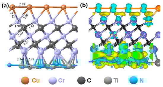
Figure 1.
Calculated solid-state properties of Cu/Cr2C/TiN. (a) Structure and (b) charge redistribution (0.06 e/Å3). Color code: yellow and blue show partially negative charge and positive charge, respectively. The unit of bond length is Å.
3. Results and Discussion
A representative structure of the Cu/Cr2C/TiN surface is illustrated in Figure 1a. The Cu(111) and TiN(100) atomic layers can be stably combined with the Cr2C atomic layer, and both Cu(001) and TiN(100) surfaces bind with Cr atoms of Cr2C material. For TiN(100), both Ti and N ions bound to Cr, which caused structural change at the surface. Since Ti and N have different charges, N would be closer with Cr than Ti because of the electrostatic attraction. Such an effect resulted in a rippled interface between TiN(100) and Cr2C(001). We then calculated the charge density difference (Figure 1b), and most of the charge difference was at the two interfaces, i.e., Cu/Cr2C and Cr2C/TiN. For the Cu/Cr2C interface, most Cu and Cr atoms are positively charged, while the interstitial regions between the two layers are negatively charged. For the Cr2C/TiN interface, there was strong charge transfer between the two layers, and strong ionic Ti-N and Cr-N bonds are identified from Figure 1b.
The resulting stronger charge distribution at the Cr2C/TiN interface seems to suggest that the Cr2C binds with TiN more strongly compared with Cu. As mentioned above, such an effect is due to the electrostatic attraction between the Cr and N atoms. The initial state, transition state, and final state structures of the Cu diffusion across the Cu/Cr2C/TiN structure are shown in Figure 2, respectively. A Cu atom was initially deposited at the vacuum side of the Cu(111) surface, and the Cu atom is expected to pass through the Cu(111) and Cr2C(100) surfaces. At the final state, Cu was bound at the vacuum side of the TiN surface. It is clear from Figure 2 that the transition state was similar to the initial state, with a calculated diffusion barrier of 0.67 eV. It can be inferred that the Cu atom can migrate inside the Cu/Cr2C/TiN structure more easily than diffusing from the vacuum to the Cu(111) surface. The difficulty of such diffusion at the Cu(111) surface may be attributed to the closely packed surface structure of Cu(111) where only tetrahedral holes can provide the ion-diffusion route.
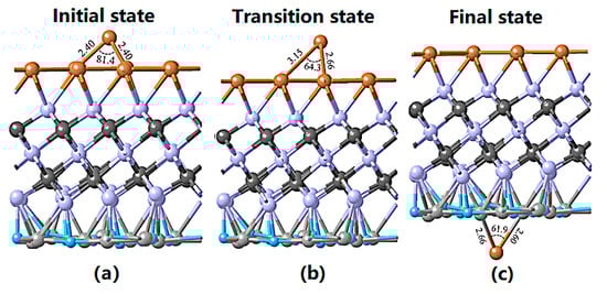
Figure 2.
Cu diffusion through the Cu/Cr2C/TiN stack in its (a) initial state, (b) transition state, and (c) final state. The units of bond length and bond angle are angstrom (Å) and degree, respectively.
Total density of states (TDOS) and partial density of states (PDOS) of the Cu/Cr2C/TiN model were also studied. Figure 3a presents the TDOS and PDOS of s, p, and d orbitals, from which the Fermi energy level is mainly occupied by the valence electron of d orbitals. This can be understood since Ti, Cr, and Cu atoms were the main components of the system, and these three elements are all transition metals which give strong d band characteristics. The metallicity of the Cu/Cr2C/TiN was therefore evident without noticeable bandgap, suggesting good electrical conductivity. Figure 3b shows the TDOS and PDOS of Cr2C, Cu, and TiN, respectively. The strong hybridization between different atomic orbitals exhibited the bonding states among Cr2C, Cu, and TiN atomic layers, and in this case the Fermi energy level was mainly contributed by d orbitals of Cr2C. The band structure of the Cu/Cr2C/TiN model is illustrated in Figure 3c. Similar to the result of the TDOS and PDOS, the band structures showed no bandgap near the Fermi level, again demonstrating its large electrical conductivity. The work function, as plotted in Figure 3d, reveals that Cu(111) had higher work function than TiN(100), meaning that the potential of the electron at Cu(111) was higher than the counterpart of TiN(100). It can be predicted from the result that electrons may be preferable to transport from the Cu(111) side to the TiN(100) side.

Figure 3.
(a) Total density of states (TDOS) of Cu/Cr2C/TiN and partial density of states (PDOS) for s, p, and d orbitals. (b) TDOS of Cu/Cr2C/TiN and PDOS for Cr2C, Cu, and TiN. (c) Band structure of Cu/Cr2C/TiN. (d) Average static potential along Z-axis.
The electronic behavior of the Cu/Cr2C/TiN stack was investigated by calculating its electrical conduction coefficients (i.e., mobility, diffusivity, and electrical conductivity) according to [39,40,41]
where μ is the Cu atom mobility; v02 is the vibration frequency of Cu during the transitional state; q is the electronic charge; T is the temperature; kB is Bolzmann’s constant; Ea is the activation energy for overcoming the diffusion barrier; δ is the migration distance of Cu; D is the diffusivity of Cu; and σ is the resulting electrical conductivity during the Cu diffusion. A is the pre-factor, given by
where QTS and QIS area the partition functions per unit volume for a transition state and an initial state, respectively. Both QTS and QIS can be possessed from the calculated vibration partition function:
where c and vi indicate the velocity of light and the vibrational frequency, respectively.
The Cu atom is assumed to migrate normally to the designed stack, and δ was therefore equal to the height of the stack in the z direction. The calculated temperature-dependent conduction coefficients of the Cu/Cr2C/TiN were subsequently compared with those of the Ag/Ti3C2/Pt stack (i.e., a typical memristive structure with MXene), as shown in Figure 4. According to Equations (1)–(3), the two key factors that affected the electronic performances of the Cu/Cr2C/TiN were T and Ea. It was found that increasing the temperature significantly increased the electrical conduction coefficients of the considered stack. Additionally, the calculated Ea of the Cu/Cr2C/TiN model was ~0.67 eV, lower than that of the Ti3C2 case (~0.85 eV). This provided the former stack with larger electrical conduction coefficients than the latter at the same temperature, which is also demonstrated in Figure 4. To further demonstrate its electrical conduction superiority, the aforementioned approaches were implemented to calculate Ea barriers of the designed stack (Cu/MXene/TiN) by using two other MXene media (i.e., V2N and Ti2N), and subsequently compared with the Ti3C2 and Cr2C cases, as illustrated in Figure 5. The calculated Ea barriers were found to be 10.64, 1.23, 0.85, and 0.67 eV for V2N, Ti2N, Ti3C2, and Cr2C, respectively. This implies that the designed stacks with Cr2C and V2N MXenes provided the strongest and weakest electrical conduction performances, respectively. It is therefore instructive to conceive that adding an extra Cr2C layer into the conventional memristor device, comprising one metal oxide layer sandwiched between Cu and TiN electrodes, can considerably accelerate the diffusion of the Cu atom inside the device and thus benefit the formation of a conductive filament (CF) along the locations of MXene nanostructures. This can remarkably improve the switching speed of the memristor and suppress the randomness of the CFs, thereby mitigating the stability and durability of the memristor device. Moreover, the resulting high electrical conductivity of the Cu/Cr2C/TiN stack is likely to lead to a lower programming voltage when compared to the Ti3C2 stack at the same temperature.
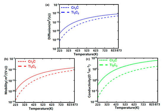
Figure 4.
Electrical conduction coefficients of Cu atoms diffusing through Cu/Cr2C/TiN including (a) diffusivity, (b) mobility, and (c) electrical conductivity with respect to temperature.
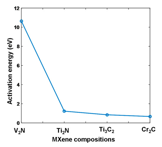
Figure 5.
Calculated activation energies as a function of the designed stacks using different MXene compositions.
4. Conclusions
We performed first-principle calculations to predict the electronic structure and electrical conduction coefficients of the Cu/Cr2C/TiN stack based on density functional theory. Implementing the Cr2C layer endowed the designed stack with metal-like characteristics and much larger conduction coefficients (i.e., mobility, diffusivity, and electrical conductivity) than the conventional Ag/Ti3C2/Pt stack due to the lower activation energy. This device is therefore capable of offering faster switching speeds, lower programming voltage, and better stability and durability than the memristor device with conventional Ti3C2 MXene.
Author Contributions
Conceptualization, L.W. and Y.T.; methodology, Q.O., J.W., L.Y., and B.-S.X.; software, B.Y. and C.Z.; validation, B.Y., C.Z., Y.J. and J.W.; writing—original draft preparation, B.Y. and L.W.; writing—review and editing, L.W. and Y.T. All authors have read and agreed to the published version of the manuscript.
Funding
This study was funded by the Shanghai Aeronautical Technological Innovation Funding (grant No. SAST2017-106, SAST2019-029), and the National Natural Science Foundation of China (grant No. 61964012, 61663030).
Conflicts of Interest
The authors declare no conflict of interest.
References
- Zhang, H. Ultrathin Two-Dimensional Nanomaterials. ACS Nano 2015, 9, 9451–9469. [Google Scholar] [CrossRef]
- Anasori, B.; Lukatskaya, M.R.; Gogotsi, Y. 2D Metal Carbides and Nitrides (MXenes) for Energy Storage. Nat. Rev. Mater. 2017, 2, 16098. [Google Scholar] [CrossRef]
- Anasori, B.; Xie, Y.; Beidaghhi, M.; Lu, J.; Hosler, B.C.; Hultman, L.; Kennt, P.R.C.; Gogotsi, Y.; Barsoum, M.W. Two-Dimensional, Ordered, Double Transition Metals Carbides (MXenes). ACS Nano 2015, 9, 9507–9516. [Google Scholar] [CrossRef] [PubMed]
- Jiang, X.; Kuklin, A.; Baev, A.; Ge, Y.; Agren, H.; Zhang, H.; Prasad, P. Two-Dimensional Mxenes: From Morphological to Optical, Electric, and Magnetic Properties and Applications. Phys. Rep. 2020, 848, 1–58. [Google Scholar] [CrossRef]
- Meshkian, R.; Tao, Q.; Dahiqvist, M.; Lu, J.; Hultman, L.; Rosen, J. Theoretical Stability and Materials Synthesis of a Chemically Ordered MAX Phase, Mo2ScAlC2, and Its Two-Dimensional Derivate Mo2ScC2 MXene. Acta Mater. 2017, 125, 476–480. [Google Scholar] [CrossRef]
- Mishra, A.; Srivastava, P.; Mizuseki, H.; Lee, K.R.; Singh, A.K. Isolation of Pristine MXene from Nb4AlC3 MAX Phase: A First-Principles Study. Phys. Chem. Chem. Phys. 2016, 18, 11073–11080. [Google Scholar] [CrossRef] [PubMed]
- Shao, B.B.; Liu, Z.F.; Zeng, G.M.; Wang, H.; Liang, Q.H.; He, Q.Y.; Cheng, M.; Zhou, C.Y.; Jiang, L.B.; Song, B. Two-Dimensional Transition Metal Carbide and Nitride (MXene) Derived Quantum Dots (QDs): Synthesis, Properties, Applications and Prospects. J. Mater. Chem. A 2020, 8, 7508–7535. [Google Scholar] [CrossRef]
- Naguib, M.; Kurtoglu, M.; Presser, V.; Lu, J.; Niu, J.; Heon, M.; Hultman, L.; Gogotsi, Y.; Barsoum, M.W. Two-Dimensional Nanocrystals Produced by Exfoliation of Ti3AlC2. Adv. Mater. 2011, 23, 4248–4253. [Google Scholar] [CrossRef]
- Sun, W.; Shah, S.; Chen, Y.; Tan, Z.; Gao, H.; Habib, T.; Radovic, M.; Green, M. Electrochemical Etching of Ti2AlC to Ti2CTx (MXene) in Low-Concentration Hydrochloric Acid Solution. J. Mater. Chem. A 2017, 5, 21663–21668. [Google Scholar] [CrossRef]
- Li, M.; Lu, J.; Luo, K.; Li, Y.; Chang, K.; Chen, K.; Zhou, J.; Rosen, J.; Hultman, L.; Eklund, P.; et al. An Element Replacement Approach by Reaction with Lewis Acidic Molten Salts to Synthesize Nanolaminated MAX Phases and Mxenes. J. Am. Chem. Soc. 2019, 141, 4730–4737. [Google Scholar] [CrossRef]
- Sarycheva, A.; Polemi, A.; Liu, Y.; Dandekar, K.; Anasori, B.; Gogotsi, Y. 2D Titanium Carbide (Mxene) for Wireless Communication. Sci. Adv. 2018, 4, eaau0920. [Google Scholar] [CrossRef] [PubMed]
- Cao, M.S.; Cai, Y.Z.; He, P.; Shu, J.C.; Cao, W.Q.; Yuan, J. 2D MXenes: Electromagnetic Property for Microwave Absorption and Electromagnetic Interference Shielding. Chem. Eng. J. 2019, 359, 1265–1302. [Google Scholar] [CrossRef]
- Pang, J.B.; Mendes, R.G.; Bachmatiuk, A.; Zhao, L.; Ta, H.Q.; Gemming, T.; Liu, H.; Liu, Z.F.; Rummeli, H. Applications of 2D MXenes in Energy Conversion and Storage Systems. Chem. Soc. Rev. 2019, 48, 72–133. [Google Scholar] [CrossRef] [PubMed]
- Liu, H.; Duan, C.Y.; Yang, C.H.; Shen, W.Q.; Wang, F.; Zhu, Z.F. A Novel Nitrite Biosensor Based on the Direct Electrochemistry of Hemoglobin Immobilized on MXene-Ti3C2. Sens. Actuators B-Chem. 2015, 218, 60–66. [Google Scholar] [CrossRef]
- Choi, G.; Shahzad, F.; Bahk, Y.M.; Jhon, Y.M.; Park, H.; Alhabeb, M.; Anasori, B.; Kim, D.S.; Koo, C.M.; Gogotsi, Y.; et al. Enhanced Terahertz Shielding of MXenes with Nano-Metamaterials. Adv. Opt. Mater. 2018, 6, 1701076. [Google Scholar] [CrossRef]
- Weng, H.M.; Ranjbar, A.; Liang, Y.Y.; Song, Z.D.; Khazaei, M.; Yunoki, S.; Arai, M.; Kawazoe, Y.; Fang, Z.; Dai, X. Large-Gap Two-Dimensional Topological Insulator in Oxygen Functionalized MXene. Phys. Rev. B 2015, 92, 075436. [Google Scholar] [CrossRef]
- Gismatulin, A.A.; Orlov, O.M.; Gritsenko, V.A.; Kruchinin, V.N.; Mizginov, D.S.; Krasnikov, G.Y. Charge Transport Mechanism in the Metal-Nitride-Oxide-Silicon Forming-Free Memristor Structure. Appl. Phys. Lett. 2020, 116, 203502. [Google Scholar]
- Gonzalez-Rosillo, J.C.; Cataalano, S.; Maggio-Aprile, I.; Gibert, M.; Obradors, X.; Palau, A.; Puig, T. Nanoscale Correlations between Metal-Insulator Transition and Resistive Switching Effect in Metallic Perovskite Oxides. Small 2020, 16, 2001307. [Google Scholar] [CrossRef]
- Yin, X.; Wang, Y.Z.; Chang, T.H.; Zhang, P.; Li, J.; Xue, P.P.; Long, Y.; Shohet, J.L.; Voyles, P.M.; Ma, Z.Q.; et al. Memristive Behavior Enabled by Amorphous-Crystalline 2D Oxide Heterostructure. Adv. Mater. 2020, 32, 20000801. [Google Scholar] [CrossRef]
- Chua, L. Memristor—The Missing Circuit Element. IEEE Trans. Circuit Theory 1971, 18, 507–519. [Google Scholar] [CrossRef]
- Strukov, D.B.; Snider, G.S.; Stewart, D.R.; Williams, R.S. The Missing Memristor Found. Nature 2008, 453, 80–83. [Google Scholar] [CrossRef]
- Yang, J.J.; Pickett, M.D.; Li, X.M.; Ohlberg, D.A.A.; Stewart, D.R.; Williams, R.S. Memristive Switching Mechanism for Metal/Oxide/Metal Nanodevices. Nat. Nanotechnol. 2008, 3, 429–433. [Google Scholar] [CrossRef] [PubMed]
- Yang, Y.C.; Gao, P.; Gaba, S.; Chang, T.; Pan, X.; Lu, W. Observation of Conducting Filament Growth in Nanoscale Resistive Memories. Nat. Commun. 2012, 13, 732. [Google Scholar] [CrossRef]
- Wang, T.Y.; Meng, J.L.; Rao, M.Y.; He, Z.Y.; Chen, L.; Zhu, H.; Sun, Q.Q.; Ding, S.J.; Bao, W.Z.; Zhou, P. Three-Dimensional Nanoscale Flexible Memristor Networks with Ultralow Power for Information Transmission and Processing Application. Nano Lett. 2020, 20, 4111–4120. [Google Scholar] [CrossRef] [PubMed]
- Xiao, X.Y.; Hu, J.; Tang, S.; Yan, K.; Gao, B.; Chen, H.L.; Zou, D.C. Recent Advances in Halide Perovskite Memristors: Materials, Structures, Mechanisms, and Applications. Adv. Mater. Technol. 2020, 5, 1900914. [Google Scholar] [CrossRef]
- Guo, Y.Y.; Hu, W.; Zhang, C.G.; Penng, Y.; Guo, Y.C. An Electronic Synapse Device based on Aluminum Nitride Memristor for Neuromorphic Computing Application. J. Phys. D-Appl. Phys. 2020, 53, 195101. [Google Scholar] [CrossRef]
- Wang, Y.Q.; Liu, X.W.; Chen, Y.H.; Xu, W.; Liang, D.K.; Gao, F.; Zhang, M.C.; Samanta, S.; Gong, X.; Lian, X.J.; et al. Manipulation of The Electrical Behaviors of Cu/MXene/SiO2/W Memristor. Appl. Phys. Express 2019, 12, 106504. [Google Scholar] [CrossRef]
- Lian, X.; Shen, X.; Zhang, M.; Xu, J.; Gao, F.; Wan, X.; Hu, E.; Guo, Y.; Zhao, J.; Tong, Y. Resistance Switching Characteristics and Mechanisms of MXene/SiO2 Structure-based Memristor. Appl. Phys. Lett. 2019, 115, 063901. [Google Scholar] [CrossRef]
- Kresse, G.; Furthmuller, J. Efficient Iterative Schemes for ab initio Total-Energy Calculations Using a Plane-Wave Basis Set. Comput. Mater. Sci. 1996, 6, 15–50. [Google Scholar] [CrossRef]
- MedeA® Is a Registered Trademark of Materials Design, Inc., Santa Fe, New Mexico, USA, 2013. Available online: https://materialsdesign.com/products (accessed on 6 July 2020).
- Kresse, G.; Joubert, D. From Ultrasoft Pseudopotentials to the Projector Augmented-Wave Method. Phys. Rev. B 1999, 56, 1758–1775. [Google Scholar] [CrossRef]
- Blochl, P.E. Projector Augmented-Wave Method. Phys. Rev. B 1994, 50, 17953–17979. [Google Scholar] [CrossRef]
- Perdew, J.P.; Burke, K.; Eunzerhof, M. Generalized Gradient Approximation Made Simple. Phys. Rev. Lett. 1996, 77, 3865–3868. [Google Scholar] [CrossRef] [PubMed]
- Perdew, J.P.; Ruzsinszky, A.; Csonka, G.I.; Vydrov, O.A.; Scuseria, G.E.; Constantin, L.A.; Zhou, X.L.; Burke, K. Restoring The Density-Gradient Expansion for Exchange in Solids and Surfaces. Phys. Rev. Lett. 2008, 100, 136406. [Google Scholar] [CrossRef] [PubMed]
- Liu, X.B.A.; Shao, X.F.; Li, F.; Zhao, M.W. Anchoring Effects of S-Terminated Ti2C MXene for Lithium-Sulfur Batteries: A First-Principles Study. Appl. Surf. Sci. 2018, 455, 522–526. [Google Scholar] [CrossRef]
- Berdiyorov, G.R. Optical Properties of Functionalized Ti3C2T2 (T = F, O, OH) MXene: First-Principles Calculations. AIP. Adv. 2016, 6, 055105. [Google Scholar] [CrossRef]
- Jonsson, H.; Mills, G.; Jacobsen, K.W. Nudged Elastic Band Method for Finding Minimum Energy Paths of Transitions; World Scientific: Singapore, 1998. [Google Scholar]
- Monkhorst, H.J.; Pack, J.D. Special Points for Brillouin-Zone Integrations. Phys. Rev. B 1976, 13, 5188–5192. [Google Scholar] [CrossRef]
- Yadav, A.; Dashora, A.; Patel, N.; Miotello, A.; Press, M.; Kothari, D.C. Study of 2D MXene Cr2C Material for Hydrogen Storage Using Density Functional Theory. Appl. Surf. Sci. 2016, 389, 88–95. [Google Scholar] [CrossRef]
- Li, H.; Wang, X.; Zhang, T.; Gong, X.; Sun, Q.; Pan, H.; Shen, Y.; Ahmad, S.; Wang, M. Layered Ruddlesden-Popper Efficient Perovskite Solar Cells with Controlled Quantum and Dielectric Confinement Introduced via Doping. Adv. Funct. Mater. 2019. [Google Scholar] [CrossRef]
- Li, B.; Guo, H.; Wang, Y.; Zhang, W.; Zhang, Q.; Chen, L.; Fan, X.; Zhang, W.; Li, Y.; Lau, W. Asymmetric MXene/Monolayer Transition Metal Dichalcogenide Heterostructures for Functional Applications. npj Comp. Mater. 2019, 5, 16–25. [Google Scholar] [CrossRef]


© 2020 by the authors. Licensee MDPI, Basel, Switzerland. This article is an open access article distributed under the terms and conditions of the Creative Commons Attribution (CC BY) license (http://creativecommons.org/licenses/by/4.0/).