In-Memory Logic Operations and Neuromorphic Computing in Non-Volatile Random Access Memory

Abstract
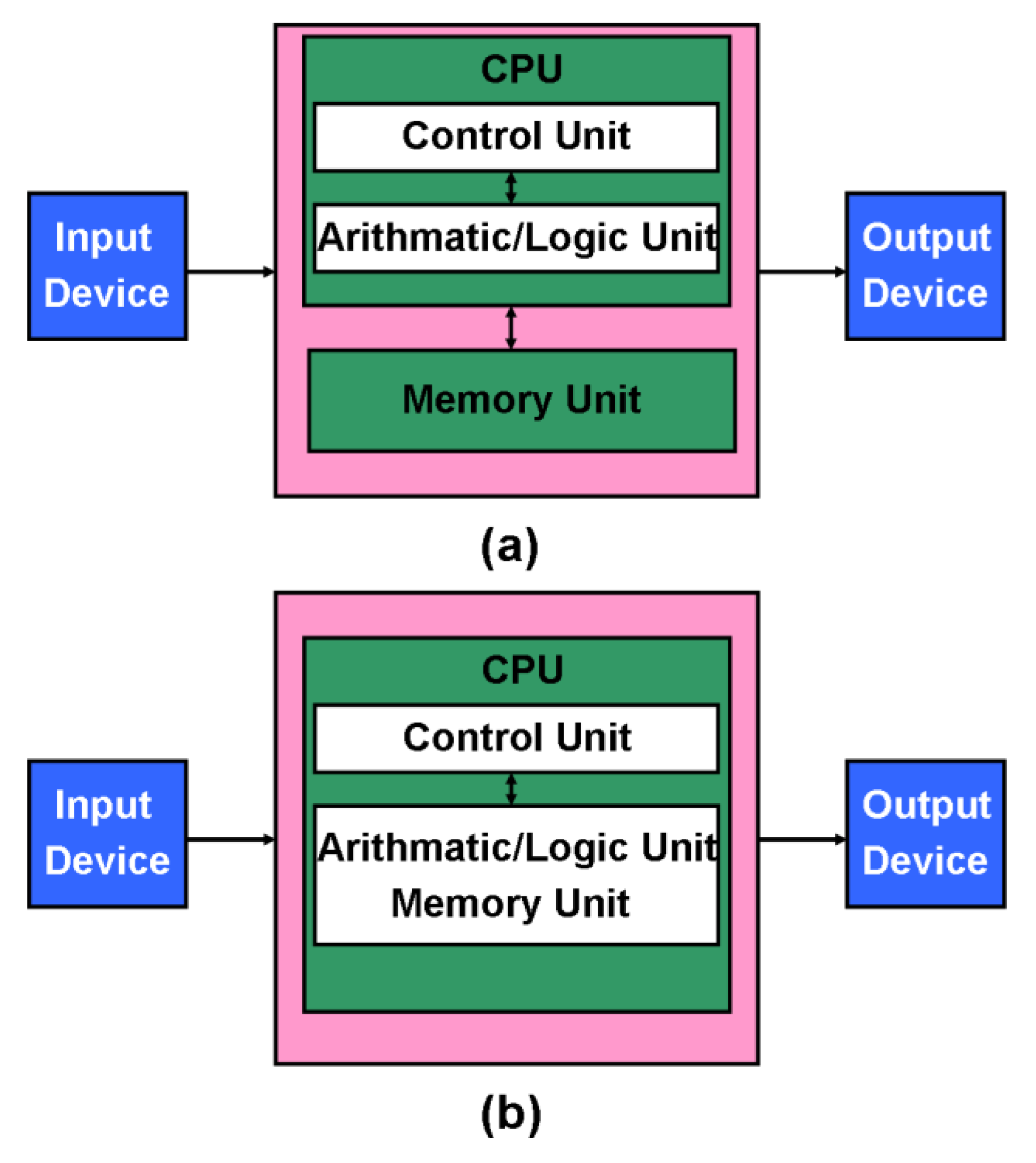
1. Introduction
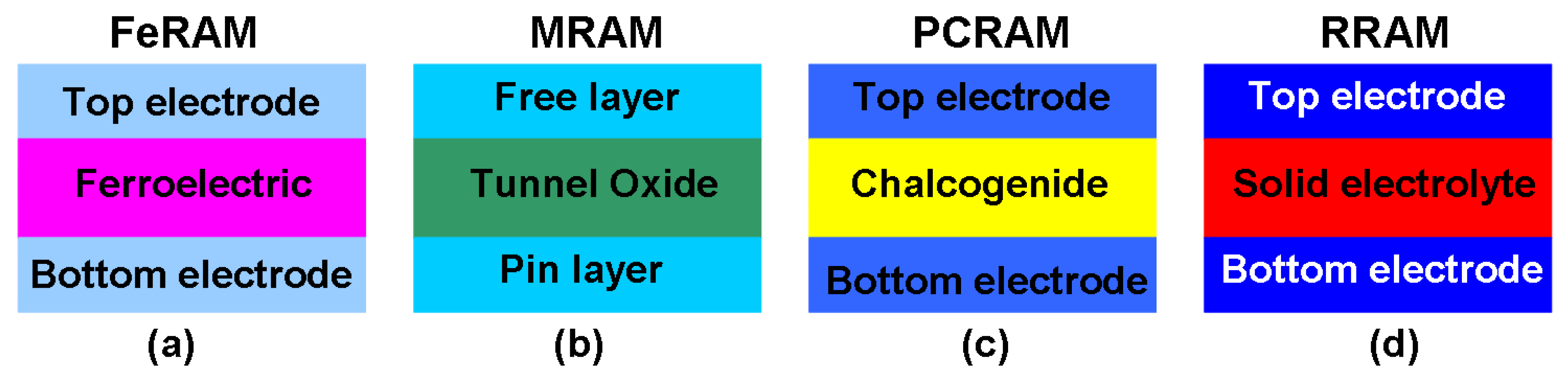
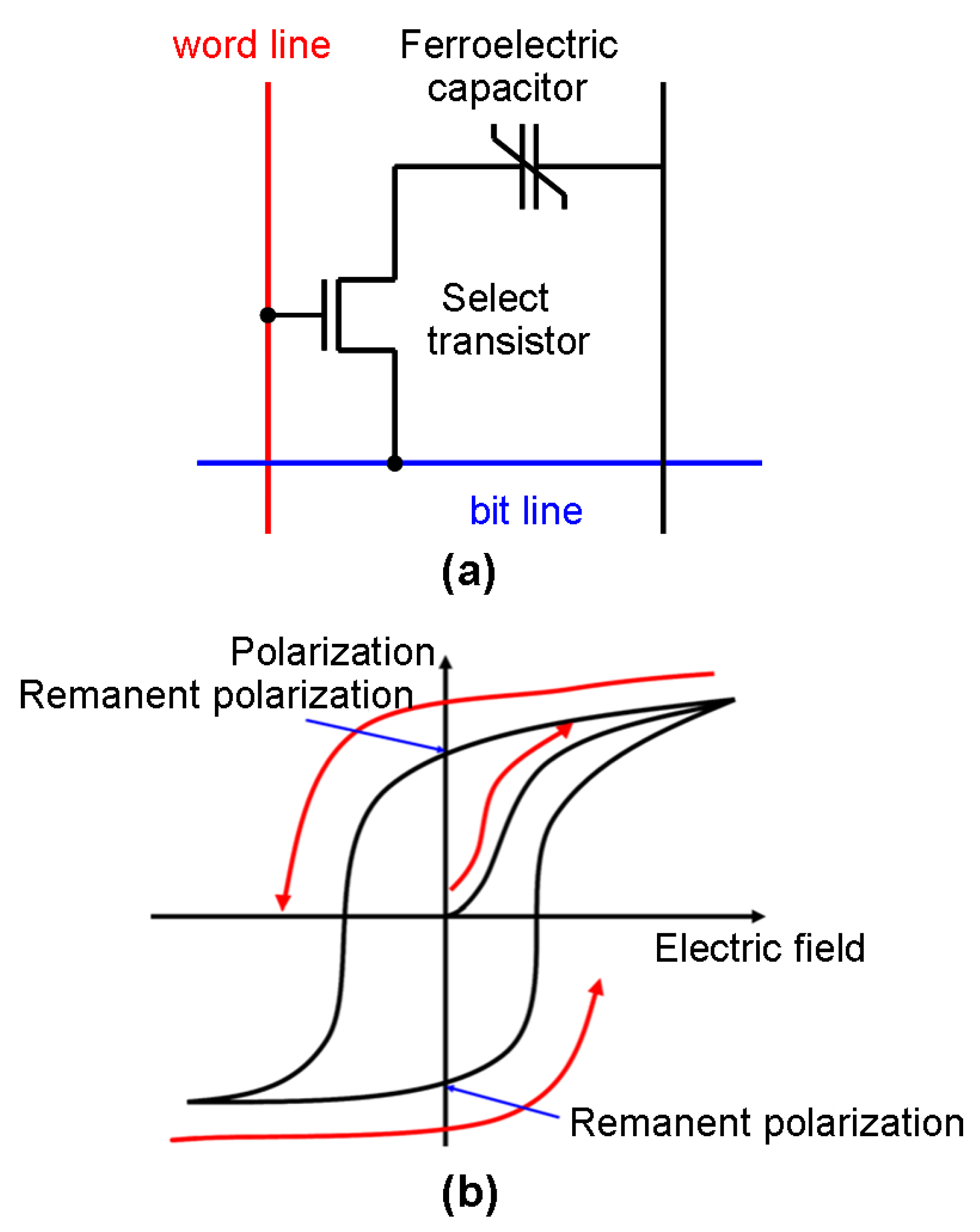
2. Logic in Ferroelectric RAM
2.1. The Technology
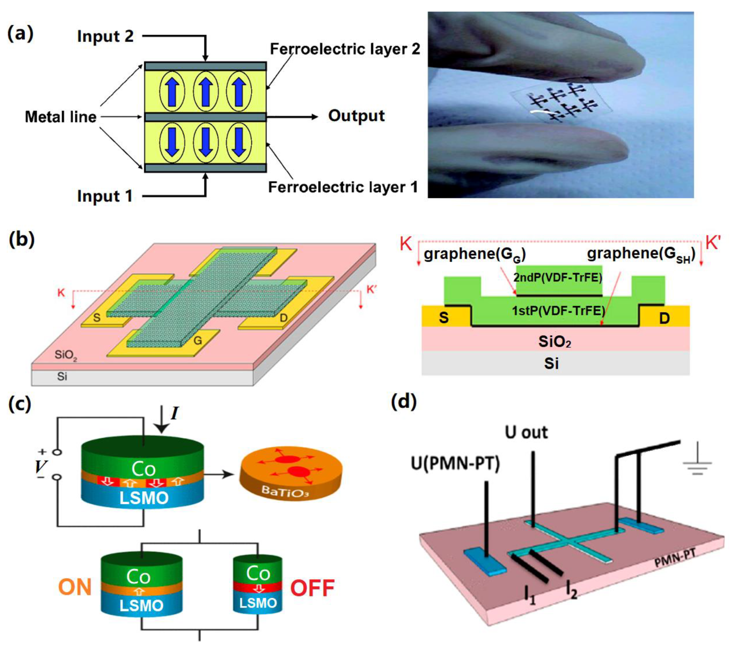
2.2. Potential for Logic Operations
2.3. Comparative Advantages and Disadvantages
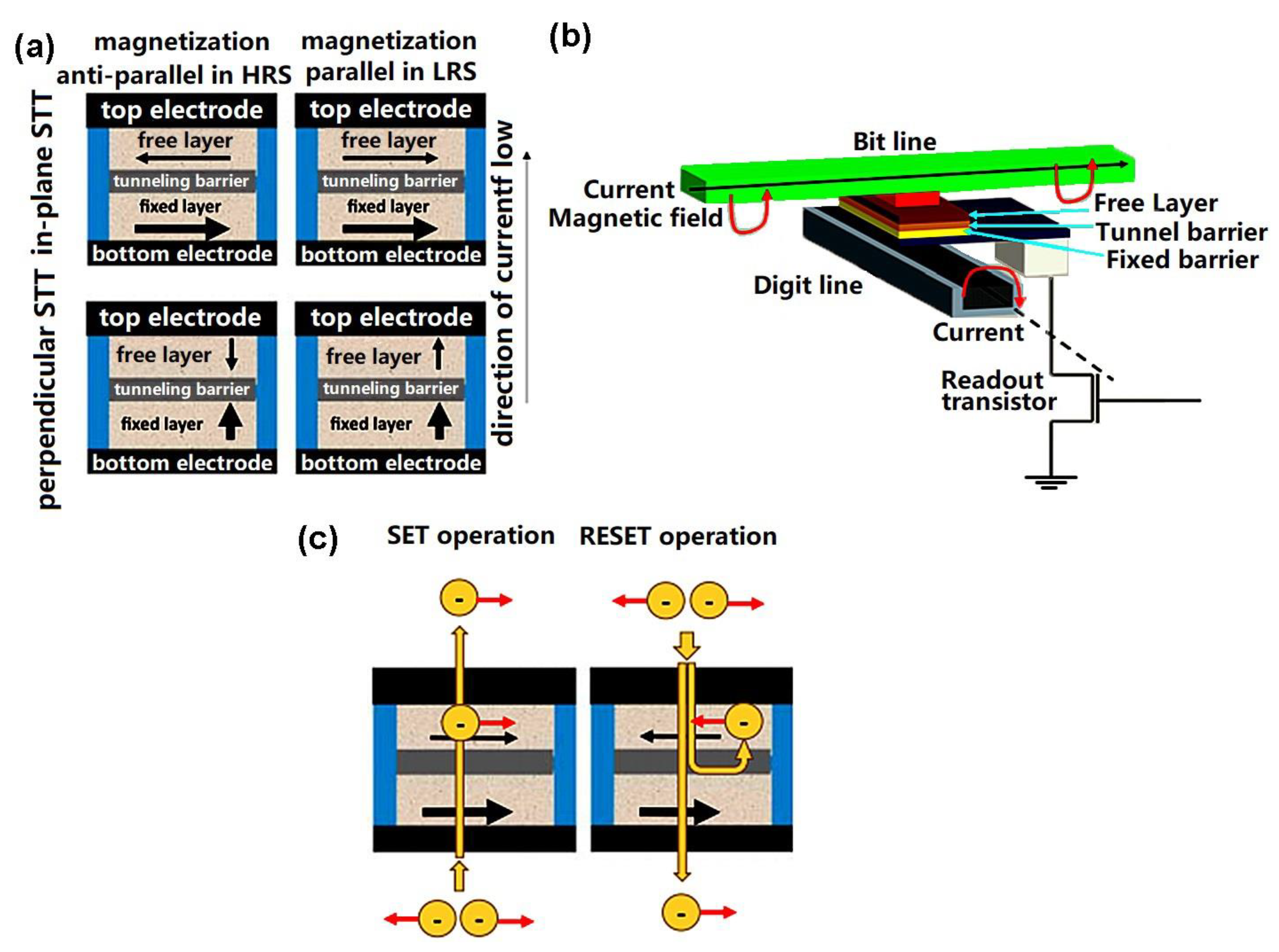
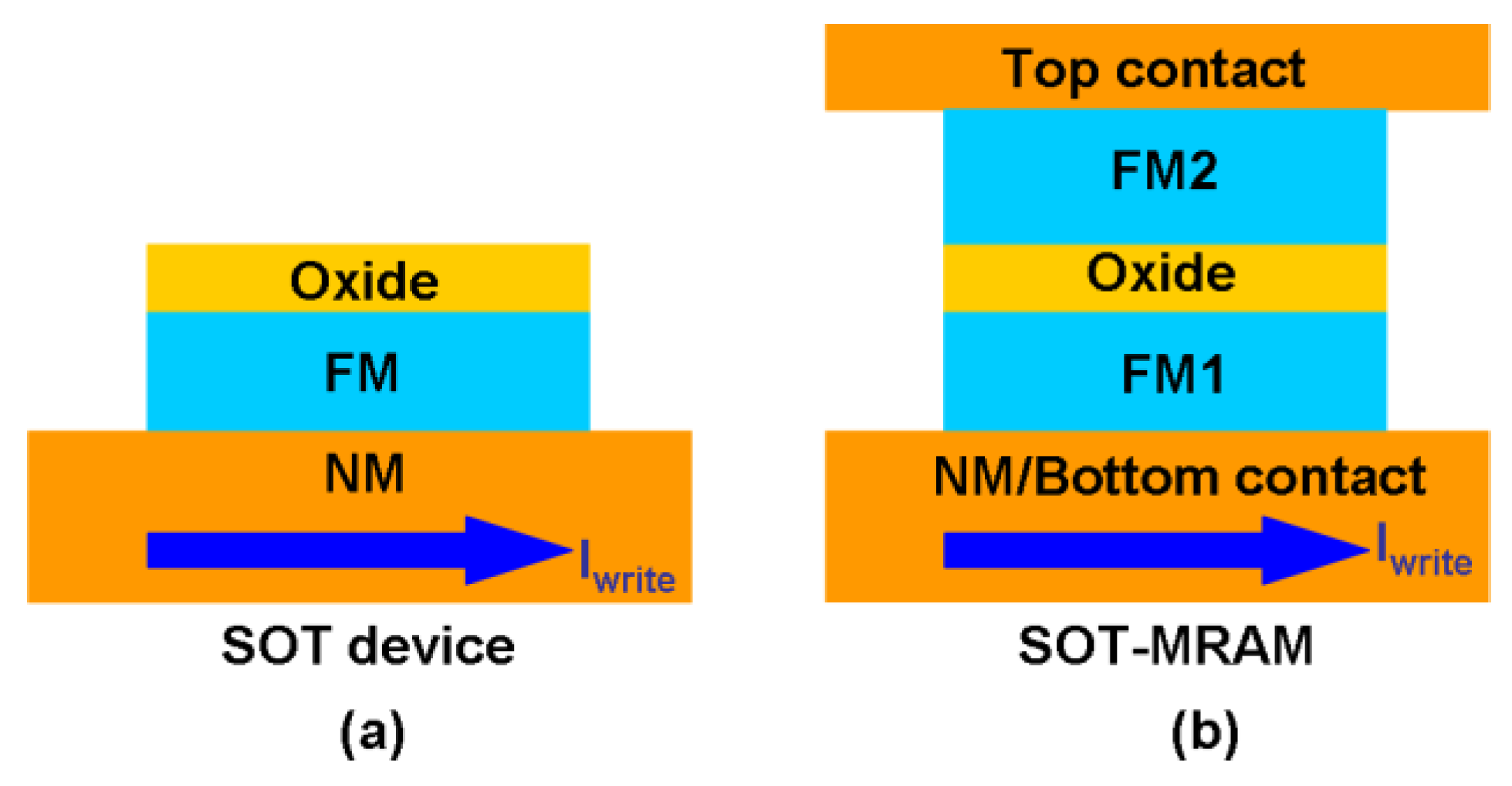
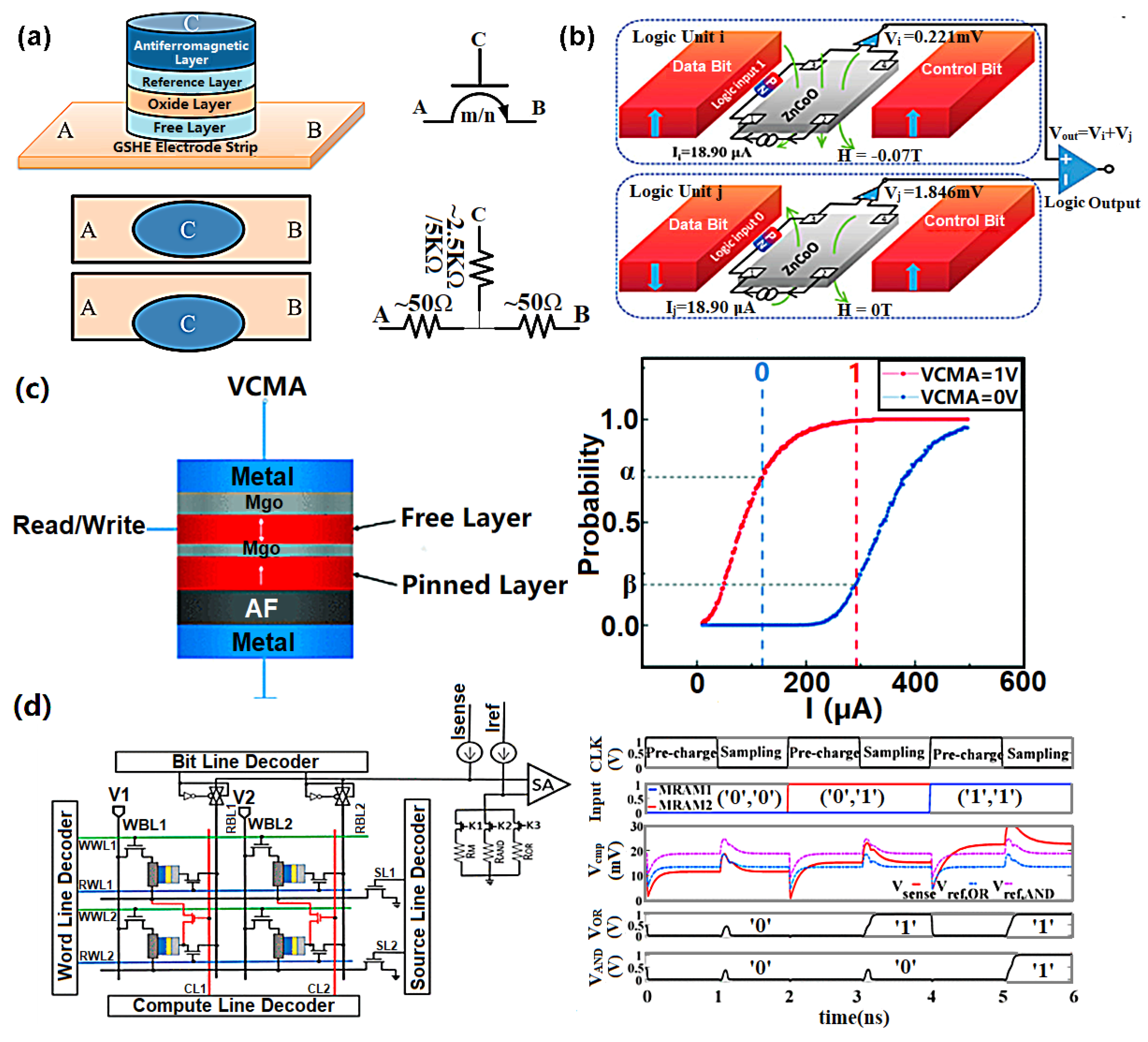
3. Logic in Magnetic RAM
3.1. The Technology
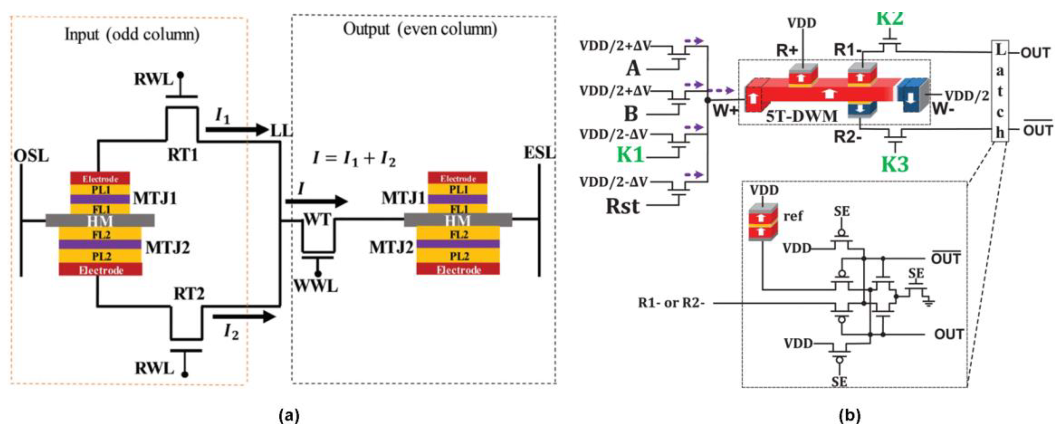
3.2. Potential for Logic Operations
3.3. Comparative Advantages and Disadvantages
4. Logic in Phase-Change RAM
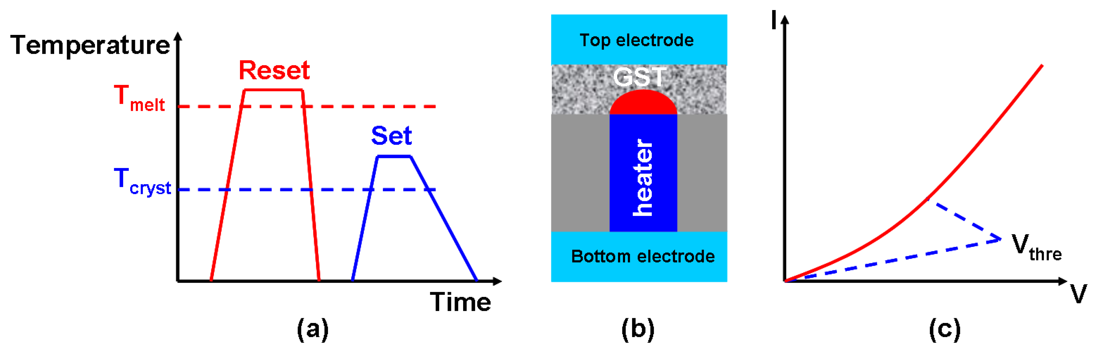
4.1. The Technology
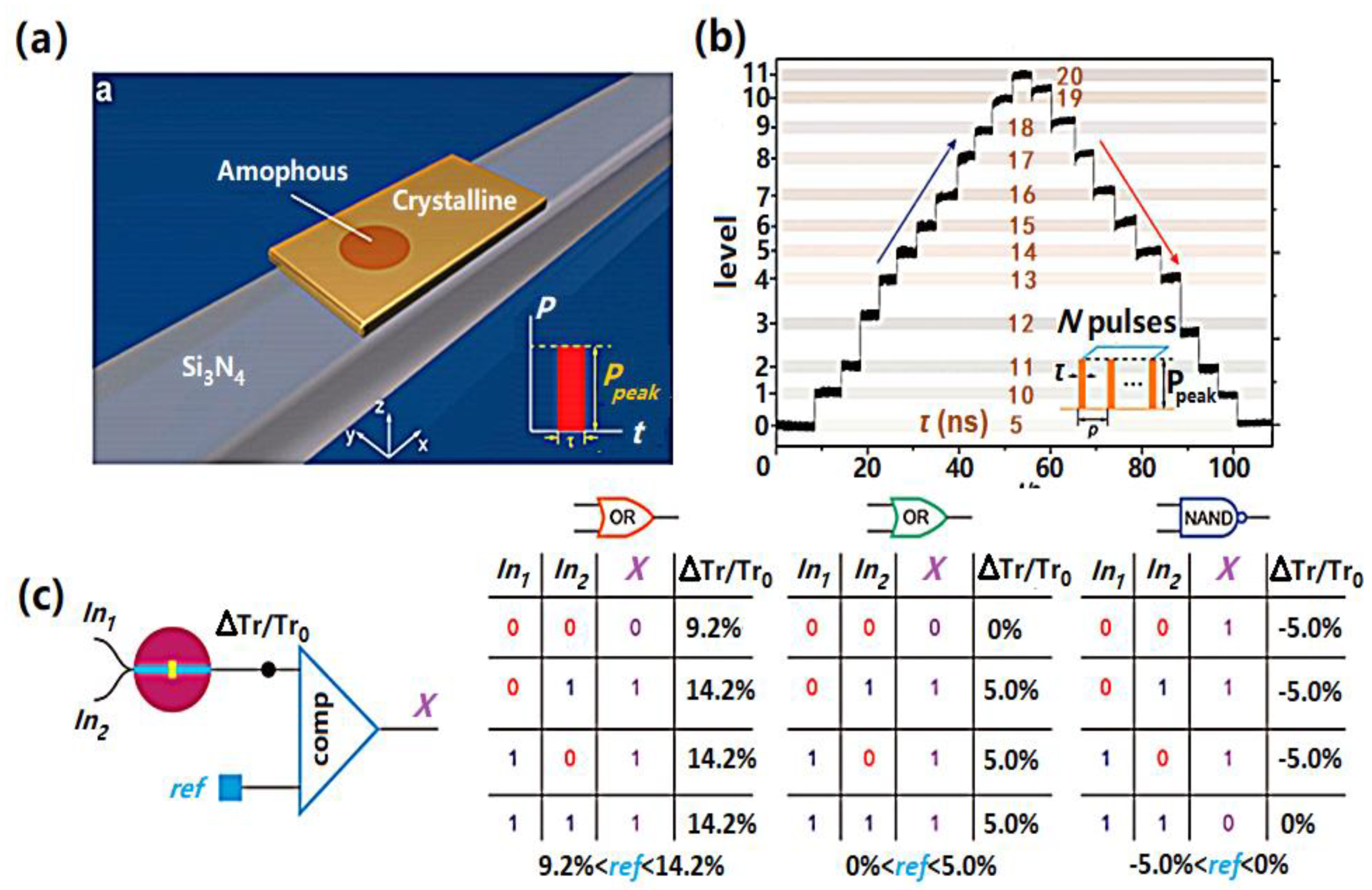
4.2. Potential for Logic Operations
4.3. Comparative Advantages and Disadvantages
5. Logic in Resistive RAM
5.1. The Technology
5.2. Potential for Logic Operations
5.3. Comparative Advantages and Disadvantages
6. Conclusions
- FeRAM offers low power consumption, a fast writing speed and good endurance but it lacks scalability. The latter is largely due to the limitations of the ferroelectric materials currently being used and this has become the main focus of research in this area, with some materials showing definite promise, such as metal oxide-doped HfOx [56,57]. A distinctive approach to tackling the scalability issue is to replace capacitor-type FeRAM with Fe field-effect transistors (FeFETs) [58,59,60], though this can impact rewrite capacity and retention time, necessitating the use of yet other materials. Ferroelectric tunnel junction (FTJ)-based devices also show promise in this area [10,63], though early tests of their potential to deliver large on-off tunnel current ratios [54] require further confirmation.
- Some forms of MRAM, for instance STT-MRAM, offer performance that is comparable, at least in terms of switching speed and endurance, to more mainstream forms of volatile RAM, such as SRAM [56]. However, other features of their performance such as their TMR ratio and reading schemes are preventing them from being properly commercialized. Additional fabrication issues indicate a need for more advanced designs and materials for MRAM, for instance, Voltage-Controlled Magnetic Anisotropy (VCMA)-based MTJs [97] and heavy metal-based GSHEs [98]. There have been notable successes in the fabrication of SOT-MRAM-based devices that overcome many of the issues associated with STT-MRAM [99], but it is clear that current density and field-free switching are still issues that will require further work and most research in this area remains largely theoretical at present.
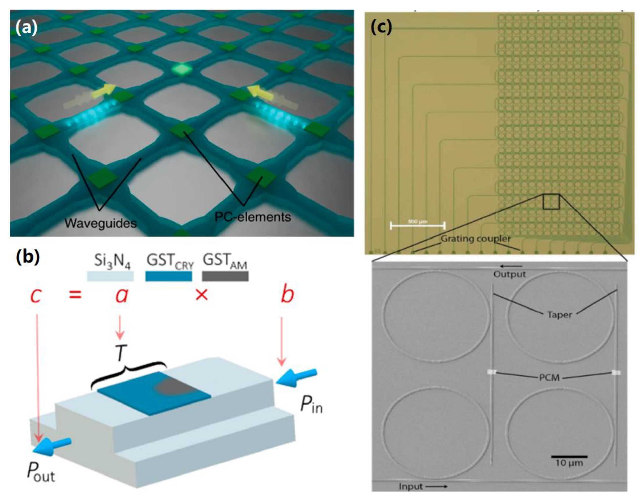
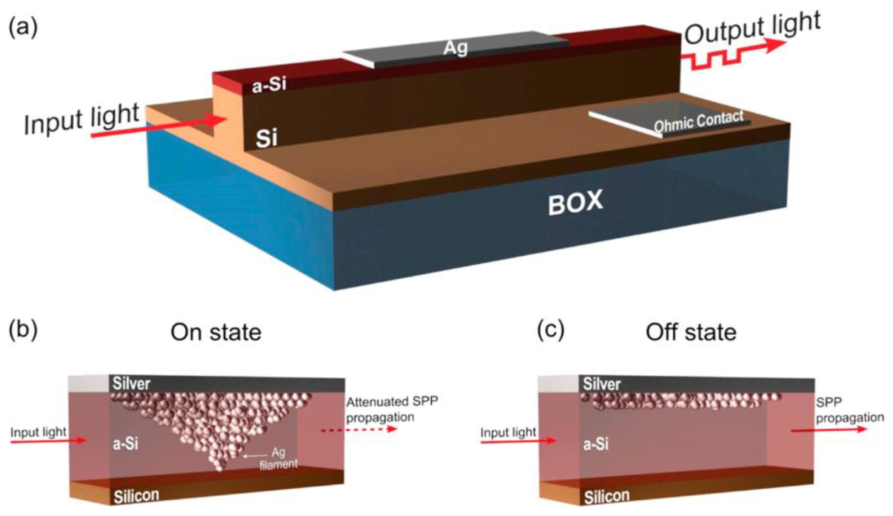
- PCRAM offers the closest non-volatile memory performance to volatile memories such as Flash and DRAM, in terms of not only switching speed and endurance but also scalability. However, high manufacturing costs make it unlikely that PCRAM will be treated as a serious competitor to Flash in the shorter term. If it can overcome its present density limitations, perhaps the most promising development in PCRAM is phase-change photonic memory, because it can use light to convey, record, and detect information, thereby circumventing the bandwidth limitations of traditional electronics and stepping around any need for extra devices for electronic-to-light conversion.
- RRAM performs well in terms of its speed, endurance and TMR ratio, but has issues in terms of retention capacity and reliability [169]. RRAM also makes use of an intrinsically stochastic switching process that can cause fluctuations in device resistance and switching voltage [170]. This, coupled with the complexity arising from its need for a forming process [171] makes RRAM an unlikely replacement for conventional volatile memory in the near future. It should be noted that MRAM also has a stochastic nature. Here, however, this has formed the basis of non-volatile stochastic computing schemes, which have traded upon its stochastic nature to gain energy advantages, improve tolerance to errors and reduce complexity and cost [89]. Attempts have also been made to turn the stochastic character of RRAM to good effect in the context of stochastic computing by producing random bit streams and reshuffle bit streams at a much lower cost. These can then be used as a basis for certain kinds of solvers and clustering algorithms [172].
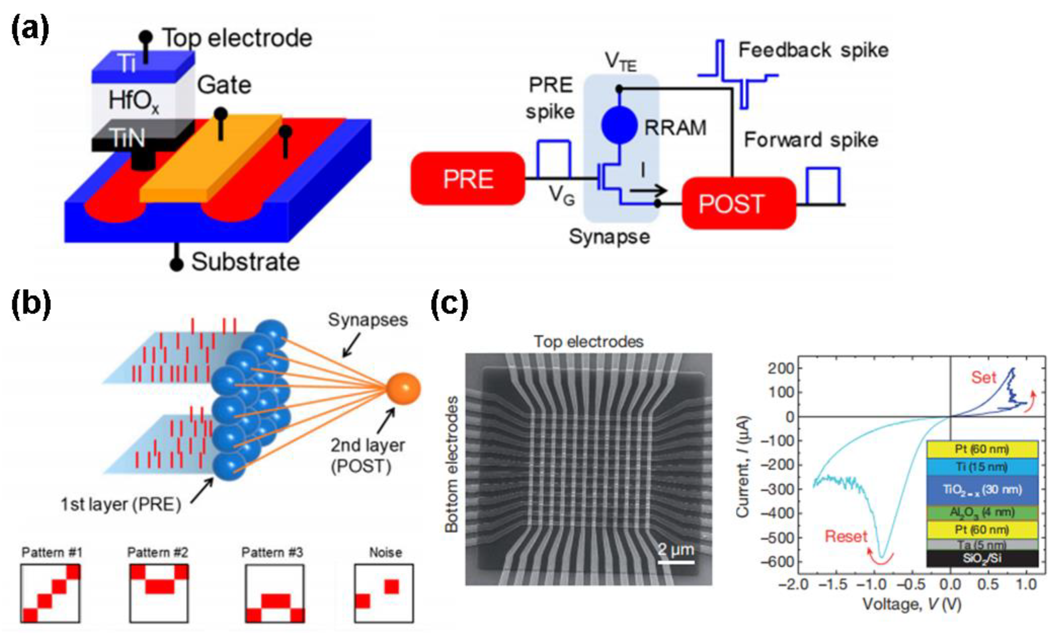
- When it comes to implementing the above as memory arrays, such arrays are currently focused on crossbar array architectures that typically make use of either phase-change materials (see [173,174]) or resistive materials (see [43], [175,176,177]). More work is still needed on realizing memory arrays using either FeRAM or MRAM, though there have already been some successes in constructing STT-MRAM memory arrays [178], and there have also been some notable moves in this direction using SOT-MRAM lately [179]. By and large, this paper has focused on discussing single device implementations and how they might be used for logic operations, but constructing larger-scale non-volatile memory arrays has also been given substantial treatment in the literature and significant progress has been made [180,181].
Author Contributions
Funding
Conflicts of Interest
References
- Mu, R.; Zeng, X. A Review of Deep Learning Research. KSII Trans. Internet Inf. Syst. 2019, 13, 1738–1764. [Google Scholar]
- Kwon, D.; Kim, H.; Kim, J.; Suh, S.C.; Kim, I.; Kim, K.J. A Survey of Deep Learning-based Network Anomaly Detection. Clust. Comput. 2017, 22, 949–961. [Google Scholar] [CrossRef]
- Ferrucci, D.A. Introduction to ‘this is watson’. IBM J. Res. Dev. 2012, 56, 1–15. [Google Scholar] [CrossRef]
- Silver, D.; Schrittwieser, J.; Simonyan, K.; Antonoglou, I.; Huang, A.; Guez, A.; Hübert, T.; Baker, L.; Lai, M.; Bolton, A.; et al. Mastering the Game of Go without Human Knowledge. Nature 2017, 550, 354–359. [Google Scholar] [CrossRef]
- Jaiswal, A.; Chakraborty, I.; Agrawal, A.; Roy, K. 8T SRAM Cell as a Multibit Dot-Product Engine for Beyond Von Neumann Computing. IEEE Trans. VLSI Syst. 2019, 27, 2556–2567. [Google Scholar] [CrossRef]
- Indiveri, G.; Liu, S.-C. Memory and Information Processing in Neuromorphic Systems. Proc. IEEE 2015, 103, 1379–1397. [Google Scholar] [CrossRef]
- Grollier, J.; Querlioz, D.; Stiles, M.D. Spintronic Nanodevices for Bioinspired Computing. Proc. IEEE 2016, 104, 2024–2039. [Google Scholar] [CrossRef]
- Ielmini, D.; Wong, H.-S.P. In-Memory Computing with Resistive Switching Devices. Nat. Electron. 2018, 1, 333–343. [Google Scholar] [CrossRef]
- Jeong, D.S.; Thomas, R.; Katiyar, R.S.; Scott, J.F.; Kohlstedt, H.; Petraru, A.; Hwang, C.S. Emerging Memory: Resistive Switching Mechanisms and Current Status. Rep. Prog. Phys. 2012, 75, 076502. [Google Scholar] [CrossRef]
- Scott, J.F. Application of Modern Ferroelectrics. Science 2007, 315, 954–959. [Google Scholar] [CrossRef]
- Hu, J.M.; Chen, L.Q.; Nan, C.W. Multiferroic Heterostructures Integrating Ferroelectric and Magnetic Materials. Adv. Mater. 2016, 28, 15–39. [Google Scholar] [CrossRef] [PubMed]
- Garcia, V.; Bibes, M. Ferroelectric Tunnel Junctions for Information Storage and Processing. Nat. Commun. 2014, 5, 4289. [Google Scholar] [CrossRef]
- Zubko, P.; Wojdel, J.C.; Hadjimichael, M.; Fernandez-Pena, S.; Sene, A.; Luk’yanchuk, I.; Triscone, J.M.; Iniguez, J. Negative Capacitance in Multidomain Ferroelectric Superlattices. Nature 2016, 534, 524–528. [Google Scholar] [CrossRef] [PubMed]
- Sbiaa, R.; Piramanayagam, S.N. Recent Developments in Spin Transfer Torque MRAM. Phys. Status Solidi (RRL) Rapid Res. Lett. 2017, 11, 1700163. [Google Scholar] [CrossRef]
- Ahmed, K.A.; Li, F.; Lua, S.Y.H.; Heng, C.H. Area-Efficient Multibit-per-Cell Architecture for Spin-Orbit-Torque Magnetic Random Access Memory with Dedicated Diodes. IEEE Magn. Lett. 2018, 9, 4303105. [Google Scholar] [CrossRef]
- Zhu, J.G. Magnetoresistive Random Access Memory: The Path to Competitiveness and Scalability. Proc. IEEE 2008, 96, 1786–1798. [Google Scholar]
- Baek, E.; Purnama, I.; You, C.Y. Limited Stochastic Current for Energy-Optimized Switching of Spin-Transfer-Torque Magnetic Random-Access Memory. Phys. Rev. Appl. 2019, 12, 064004. [Google Scholar] [CrossRef]
- Li, X.; Sasaki, T.; Grezes, C.; Wu, D.; Wong, K.L.; Bi, C.; Ong, P.-V.; Ebrahimi, F.; Yu, G.; Kioussis, N.; et al. Predictive Materials Design of Magnetic Random-Access Memory Based on Nanoscale Atomic Structure and Element Distribution. Nano Lett. 2019, 19, 8621–8629. [Google Scholar] [CrossRef]
- Wong, H.S.P.; Raoux, S.; Kim, S.; Liang, J.L.; Reifenberg, J.P.; Rajendran, B.; Asheghi, M.; Goodson, K.E. Phase Change Memory. Proc. IEEE 2010, 98, 2201–2227. [Google Scholar] [CrossRef]
- Burr, G.W.; Breitwisch, M.J.; Franceschini, M.; Garetto, D.; Gopalakrishnan, K.; Jackson, B.; Kurdi, B.; Lam, C.; Lastras, L.A.; Padilla, A.; et al. Phase Change Memory Technology. J. Vac. Sci. Technol. B 2010, 28, 223–262. [Google Scholar] [CrossRef]
- Yu, S.M. Neuro-Inspired Computing with Emerging Nonvolatile Memory. Proc. IEEE 2018, 106, 260–285. [Google Scholar] [CrossRef]
- Rao, F.; Ding, K.; Zhou, Y.; Zheng, Y.; Xia, M.; Lv, S.; Song, Z.; Feng, S.; Ronneberger, I.; Mazzarello, R.; et al. Reducing the Stochasticity of Crystal Nucleation to Enable Subnanosecond Memory Writing. Science 2017, 358, 1423–1426. [Google Scholar] [CrossRef]
- Bertolazzi, S.; Bondavalli, P.; Roche, S.; San, T.; Choi, S.Y.; Columbo, L.; Bonaccorso, F.; Samori, P. Nonvolatile Memories Based on Graphene and Related 2D Materials. Adv. Mater. 2019, 31, 1806663. [Google Scholar] [CrossRef] [PubMed]
- Waser, R.; Aono, M. Nanoionics-based Resistive Switching Memories. Nat. Mater. 2007, 6, 833–840. [Google Scholar] [CrossRef] [PubMed]
- Wong, H.S.P.; Lee, H.Y.; Yu, S.M.; Chen, Y.S.; Wu, Y.; Chen, P.S.; Lee, B.; Chen, F.T.; Tsai, M.J. Metal-Oxide RRAM. Proc. IEEE 2012, 100, 1951–1970. [Google Scholar] [CrossRef]
- Wedig, A.; Lübben, M.; Cho, D.Y.; Moors, M.; Skaja, K.; Rana, V.; Hasegawa, T.; Adepalli, K.K.; Yildiz, B.; Waser, R.; et al. Nanoscale Cation Motion in TaOx, HfOx and TiOx Memristive Systems. Nat. Nanotechnol. 2016, 30, 67–74. [Google Scholar]
- Choi, J.; Han, J.S.; Hong, K.; Kim, S.Y.; Jang, H.W. Organic-Inorganic Hybrid Halide Perovskites for Memories, Transistors, and Artificial Synapse. Adv. Mater. 2018, 136, 1704002. [Google Scholar] [CrossRef]
- Hao, C.; Wen, F.; Xiang, J.; Yuan, S.; Yang, B.; Li, L.; Wang, W.; Zeng, Z.; Wang, L.; Liu, Z.; et al. Liquid-Exfoliated Black Phosphorous Nanosheet Thin Films for Flexible Resistive Random Access Memory Applications. Adv. Funct. Mater. 2016, 26, 2016–2024. [Google Scholar] [CrossRef]
- Guo, M.F.; Jiang, J.Y.; Qian, J.F.; Liu, C.; Ma, J.; Nan, C.W.; Shen, Y. Flexible Robust and High-Density FeRAM from Array of Organic Ferroelectric Nano-Lamellae by Self-Assembly. Adv. Sci. 2019, 6, 1801931. [Google Scholar] [CrossRef]
- Rzeszut, P.; Skowronski, W.; Zietek, S.; Wrona, J.; Stobiecki, T. Multi-bit MRAM Storage Cells Utilizing Serially Connected Perpendicular Magnetic Tunnel Junctions. J. Appl. Phys. 2019, 125, 025704. [Google Scholar] [CrossRef]
- Lee, J.H.; Lim, D.H.; Jeong, H.; Ma, H.M.; Shi, L.P. Exploring Cycle-to-Cycle and Device-to-Device Variation Tolerance in MLC Storage-based Neural Network Training. IEEE Trans. Electron Devices 2019, 66, 2172–2178. [Google Scholar] [CrossRef]
- Qin, S.J.; Jiang, Z.Z.; Li, H.T.; Fujii, S.; Lee, D.; Wong, S.S.; Wong, H.S.P. Next-Generation Ultrahigh-Density 3-D Vertical Resistive Switching Memory (VRSM)-Part I: Accurate and Computationally Efficient Modeling. IEEE Trans. Electron Devices 2019, 66, 5139–5146. [Google Scholar] [CrossRef]
- Chiu, C.H.; Huang, C.W.; Hsieh, Y.H.; Chen, J.Y.; Chang, C.F.; Chu, Y.H.; Wu, W.W. In-situ TEM Observation of Multilevel Storage Behavior in Low Power FeRAM Device. Nano Energy 2017, 34, 103–110. [Google Scholar] [CrossRef]
- Shadmana, A.; Zhu, J.G. High-Speed STT MRAM Incorporating Antiferromagnetic Layer. Appl. Phys. Lett. 2019, 114, 022403. [Google Scholar] [CrossRef]
- Cho, J.Y.; Kim, D.; Park, Y.J.; Yang, T.Y.; Lee, Y.Y.; Joo, Y.C. The Phase-Change Kinetics of Amorphous Ge2Sb2Te5 and Device Characteristics Investigated by Thin Film Mechanics. Acta Mater. 2015, 94, 143–151. [Google Scholar] [CrossRef]
- Zhao, X.L.; Zhang, X.M.; Shang, D.S.; Wu, Z.H.; Xiao, X.H.; Chen, R.; Tang, C.Y.; Liu, J.C.; Li, W.Q.; Lv, H.B.; et al. Uniform, Fast, and Reliable LixSiOy-based Resistive Switching Memory. IEEE Electron Device Lett. 2019, 40, 554–557. [Google Scholar] [CrossRef]
- Iida, M.; Koga, M.; Inoue, K.; Amagasaki, M.; Ichida, Y.; Saji, M.; Iida, J.; Sueyoshi, T. A Genuine Power-Gatable Reconfigurable Logic Chip with FeRAM Cells. IEICE Trans. Electron. 2011, E94C, 548–556. [Google Scholar] [CrossRef]
- Park, J.; Lee, M.; Kim, S.; Ju, M.; Hong, J. MH Cache: A Multi-Retention STT-RAM-based Low-Power Last-Level Cache for Mobile Hardware Rendering Systems. ACM Trans. Archit. Code Optim. 2019, 16, 1–26. [Google Scholar] [CrossRef]
- Hwang, I.; Cho, Y.J.; Lee, M.J.; Jo, M.H. The Role of Contact Resistance in GeTe and Ge2Sb2Te5 Nanowire Phase Change Memory Reset Switching Current. Appl. Phys. Lett. 2019, 106, 193106. [Google Scholar] [CrossRef]
- Lin, C.C.; Liou, H.Y.; Hung, P.H.; Chu, S.Y.; Huang, C.Y.; Hong, C.S. Effects of Film Orientation on Power Consumption, Thermal Stability, and Reliability of Aluminum Nitride Resistive Random Access Memory Devices. IEEE Trans. Electron Devices 2019, 66, 4716–4721. [Google Scholar] [CrossRef]
- Nomura, Y.; Nomura, K.; Kinoshita, K.; Kawae, T.; Morimoto, A. Retention Properties with High-Temperature Resistance in (bi, Pr)(Fe, Mn)O3 Thin Film Capacitor. Phys. Status Solidi (RRL) Rapid Res. Lett. 2014, 8, 536–539. [Google Scholar] [CrossRef]
- Senni, S.; Torres, L.; Sassatelli, G.; Gamatie, A. Non-volatile Processor based on MRAM for Ultra-Low-Power IoT Devices. ACM J. Emerg. Technol. Comput. Syst. 2017, 13, 1–17. [Google Scholar] [CrossRef]
- Elliott, S.R. Chalcogenide Phase-Change Materials: Past and Future. Int. J. Appl. Glas. Sci. 2015, 6, 15–18. [Google Scholar] [CrossRef]
- Xiang, Y.C.; Huang, P.; Zhao, Y.D.; Zhao, M.R.; Gao, B.; Wu, H.Q.; Qian, H.; Liu, X.Y.; Kang, J.F. Impacts of State Instability and Retention Failure of Filamentary Analog RRAM on the Performance of Deep Neural Network. IEEE Trans. Electron Devices 2019, 66, 4517–4522. [Google Scholar] [CrossRef]
- Saeideh, S.; Drechsler, R. In-Memory Computing: The Integration of Storage and Processing. In Information Storage; Springer: Cham, Switzerland, 2020; pp. 79–110. [Google Scholar]
- Kato, H.; Nozawa, H. Proposal for 1T/1C Ferroelectric Random Access Memory with Multiple Storage and Application to Functional Memory. Jpn. J. Appl. Phys. 2003, 42, 6000–6002. [Google Scholar] [CrossRef]
- Wang, L.; Yang, C.H.; Wen, J. Physical Principles and Current Status of Emerging Non-Volatile Solid State Memories. Electron. Mater. Lett. 2014, 11, 505–543. [Google Scholar] [CrossRef]
- Takasu, H.; Fujimori, Y.; Nakamura, T.; Kimura, H.; Hanyu, T.; Kameyama, M. Ferroelectric Non-Volatile Logic Devices. Integr. Ferroelectr. 2004, 61, 83–88. [Google Scholar] [CrossRef]
- Li, Y.; Ding, Y.Q.; Liu, X.; Yan, J.F.; Lin, Y.Y.; Tang, T.G. A Verification of Nonvolatile Programmable Logic Device. Integr. Ferroelectr. 2007, 89, 62–68. [Google Scholar] [CrossRef]
- Horie, S.; Noda, K.; Yamada, H.; Matsushige, K. Flexible Programmable Logic Gate Using Organic Ferroelectric Multilayer. Appl. Phys. Lett. 2007, 91, 193506. [Google Scholar] [CrossRef]
- Kim, W.Y.; Kim, H.D.; Jeon, G.J.; Kang, I.K.; Shim, H.B.; Kim, T.H.; Lee, H.C. Bistable Memory and Logic-Gate Devices Fabricated by Intercrossed Stacking of Graphene-Ferroelectric Hybrid Ribbons. Micro Nano Lett. 2016, 11, 356–359. [Google Scholar] [CrossRef]
- Wang, Z.H.; Zhao, W.S.; Kang, W.; Zhang, Y.; Klein, J.O.; Ravelosona, D.; Zhang, Y.G.; Chappert, C. Nonvolatile Boolean Logic Block Based on Ferroelectric Tunnel Memristor. IEEE Trans. Magn. 2014, 50, 9100604. [Google Scholar] [CrossRef]
- Yang, M.Y.; Deng, Y.C.; Wu, Z.H.; Cai, K.M.; Edmonds, K.W.; Li, Y.C.; Sheng, Y.; Wang, S.M.; Cui, Y.; Luo, J.; et al. Spin Logic Devices via Electric Field Controlled Magnetization Reversal by Spin-Orbit Torque. IEEE Electron Device Lett. 2019, 40, 1554–1557. [Google Scholar] [CrossRef]
- Eshita, T.; Wang, W.S.; Nomura, K.; Nakamura, K.; Saito, H.; Yamaguchi, H.; Mihara, S.; Hikosaka, Y.; Kataoka, Y.; Kojima, M. Development of Highly Reliable Ferroelectric Random Access Memory and Its Internet of Things Applications. Jpn. J. Appl. Phys. 2018, 57, 11UA01. [Google Scholar] [CrossRef]
- Muller, J.; Yurchuk, E.; Schlosser, T.; Paul, J.; Hoffmann, R.; Muller, S.; Martin, D.; Slesazeck, S.; Polakowski, P.; Sundqvist, J.; et al. Ferroelectricity in HfO2 enables nonvolatile data storage in 28 nm HKMG. In Proceedings of the 2012 Symposium on VLSI Technology (VLSIT), Honolulu, HI, USA, 12–14 June 2012; pp. 25–26. [Google Scholar]
- Muller, J.; Boscke, T.S.; Muller, S.; Yurchuk, E.; Polakowski, P.; Paul, J.; Martin, D.; Schenk, T.; Khullar, K.; Kersch, A.; et al. Ferroelectric Hafnium Oxide: A CMOS-Compatible and Highly Scalable Approach to Future Ferroelectric Memories. In Proceedings of the 2013 IEEE International Electron Devices Meeting, Washington, DC, USA, 9–11 December 2013. [Google Scholar]
- Chen, A. A Review of Emerging Non-Volatile Memory (NVM) Technologies and Applications. Solid State Electron. 2016, 125, 25–38. [Google Scholar] [CrossRef]
- Muller, J.; Boscke, T.S.; Brauhaus, D.; Schroder, U.; Bottger, U.; Sundqvist, J.; Kucher, P.; Mikolajick, T.; Frey, L. Ferroelectric Zr0.5Hf0.5O2 Thin Films for Nonvolatile Memory Applications. Appl. Phys. Lett. 2011, 99, 112901. [Google Scholar] [CrossRef]
- Muller, J.; Schroder, U.; Boscke, T.S.; Muller, I.; Botter, U.; Wilde, L.; Sundqvist, J.; Lemberger, M.; Kucher, P.; Mikolajick, T.; et al. Ferroelectricity in Yttrium-Doped Hafnium Oxide. J. Appl. Phys. 2011, 110, 114113. [Google Scholar] [CrossRef]
- Sakai, S.; Zhang, W.; Takahashi, M. Dynamic Analog Characteristics of 109 Cycle-Endurance Low-Voltage Nonvolatile Ferroelectric-Gate Memory Transistors. In Proceedings of the 2017 IEEE International Memory Workshop (IMW), Monterey, CA, USA, 14–17 May 2017; pp. 1–4. [Google Scholar]
- Ahmedullah, A.; Breyer, E.T.; Chen, A.; Chen, X.M.; Datta, S.; Gupta, S.K.; Hoffmann, M.; Hu, X.S.; Ionescu, A.M.; Jerry, M.; et al. Computing with ferroelectric FETs: Devices, models, systems, and applications. In Proceedings of the 2018 Design, Automation & Test in Europe Conference & Exhibition (DATE), Dresden, Germany, 19–23 March 2018; pp. 1–4. [Google Scholar]
- Tsymbal, E.Y.; Kohlstedt, H. Tunneling Across a Ferroelectric. Science 2006, 313, 181–183. [Google Scholar] [CrossRef]
- Yamada, H.; Tsurumaki-Fukuchi, A.; Kobayashi, M.; Nagai, T.; Toyosaki, Y.; Kumigashira, H.; Sawa, A. Strong Surface-Termination Effect on Electroresistance in Ferroelectric Tunnel Junctions. Adv. Funct. Mater. 2015, 25, 2708–2714. [Google Scholar] [CrossRef]
- Slesazeck, S.; Mikolajick, T. Nanoscale Resistive Switching Memory Devices: A Review. Nanotechnology 2019, 30, 352003. [Google Scholar] [CrossRef]
- Prejbeanu, I.L.; Bandiera, S.; Herault, J.A.; Sousa, R.C.; Dieny, B.; Nozieres, J.P. Thermally Assisted MRAMs: Ultimate Scalability and Logic Functionalities. J. Phys. D Appl. Phys. 2013, 46, 074002. [Google Scholar] [CrossRef]
- Prejbeanu, I.L.; Sousa, R.C.; Dieny, B.; Nozieres, J.P.; Bandiera, S.; Herault, J.A.; Stainer, Q.; Lornbard, L.; Ducruet, C.; Conraux, Y.; et al. Scalability and Logic Functionalities of TA-MRAMs. In Proceedings of the 2013 IEEE 11th International New Circuits and Systems Conference (NEWCAS), Paris, France, 16–19 June 2013; pp. 1–4. [Google Scholar]
- Dieny, B.; Sousa, R.; Bandiera, S.; Souza, M.C.; Auffret, S.; Rodmacq, B.; Nozieres, J.P.; Herault, J.; Gapihan, E.; Prejbeanu, I.L.; et al. Extend Scalability and Functionalities of MRAM based on Thermally Assisted Writing. In Proceedings of the 2011 International Electron Devices Meeting, Washington, DC, USA, 5–7 December 2011; pp. 1–4. [Google Scholar]
- Chatterjee, J.; Chavent, A.; Fettar, F.; Auffret, S.; Ducruet, C.; Joumard, I.; Vila, L.; Sousa, R.C.; Prejbeanu, L.; Dieny, B. Reduced Thermal Variation of Perpendicular Magnetic Anisotropy in Magnetically Stiffened Dual-W Composite Storage Layer for Spin-Transfer-Torque Magnetic Random-Access Memory. Phys. Rev. Appl. 2011, 12, 044043. [Google Scholar] [CrossRef]
- Radhakrishnan, G.; Yoon, Y.; Sachdev, M. A Parametric DFT Scheme for STT-MRAMs. IEEE Trans. VLSI 2019, 27, 1685–1696. [Google Scholar] [CrossRef]
- Sayed, N.; Bishnoi, R.; Tahoori, M.B. Fast and Reliable STT-MRAM Using Nonuniform and Adaptive Error Detecting and Correcting Scheme. IEEE Trans. VLSI 2019, 27, 1329–1342. [Google Scholar] [CrossRef]
- Ramaswamy, R.; Lee, J.M.; Cai, K.; Yang, H. Recent Advances in Spin-Orbit Torques: Moving Towards Device Applications. Appl. Phys. Rev. 2018, 5, 031107. [Google Scholar] [CrossRef]
- Chernyshov, A.; Overby, M.; Liu, X.; Furdyna, J.K.; Lyanda-Geller, Y.; Rokhinson, L.P. Evidence for Reversible Control of Magnetization in a Ferromagnetic Material by Means of Spin–Orbit Magnetic Field. Nat. Phys. 2009, 5, 656–659. [Google Scholar] [CrossRef]
- Miron, I.M.; Gaudin, G.; Auffret, S.; Rodmacq, B.; Schuhl, A.; Pizzini, S.; Vogel, J.; Gambardella, P. Current-Driven Spin Torque Induced by the Rashba Effect in a Ferromagnetic Metal Layer. Nat. Mater. 2010, 9, 230–234. [Google Scholar] [CrossRef]
- Ioan Mihai, M.; Garello, K.; Gaudin, G.; Zermatten, P.; Costache Marius, V.; Auffret, S.; Bandiera, S.; Rodmacq, B.; Schuhl, A.; Gambardella, P. Perpendicular Switching of a Single Ferromagnetic Layer Induced by In-Plane Current Injection. Nature 2011, 476, 189–193. [Google Scholar]
- Liu, L.; Pai, C.F.; Li, Y.; Tseng, H.W.; Ralph, D.C.; Buhrman, R.A. Spin-Torque Switching with The Giant Spin Hall Effect of Tantalum. Science 2012, 336, 555–558. [Google Scholar] [CrossRef]
- Luqiao, L.; Lee, O.J.; Gudmundsen, T.J.; Ralph, D.C.; Buhrman, R.A. Current-Induced Switching of Perpendicularly Magnetized Magnetic Layers Using Spin Torque from The Spin Hall Eeffect. Phys. Rev. Lett. 2012, 109, 096602. [Google Scholar]
- Luqiao, L.; Moriyama, T.; Ralph, D.C.; Buhrman, R.A. Spin-Torque Ferromagnetic Resonance Induced by the Spin Hall Effect. Phys. Rev. Lett. 2011, 106, 036601. [Google Scholar]
- Aradhya, S.V.; Rowlands, G.E.; Oh, J.; Ralph, D.C.; Buhrman, R.A. Nanosecond-Timescale Low Energy Switching of In-Plane Magnetic Tunnel Junctions through Dynamic Oersted-Field-Assisted Spin Hall Effect. Nano Lett. 2016, 16, 5987–5992. [Google Scholar] [CrossRef] [PubMed]
- Kevin, G.; Avci, C.O.; Miron, I.M.; Baumgartner, M.; Ghosh, A.; Auffret, S.; Boulle, O.; Gaudin, G.; Gambardella, P. Ultrafast Magnetization Switching by Spin-Orbit Torques. Appl. Phys. Lett. 2014, 105, 212402. [Google Scholar]
- See-Hun, Y.; Ryu, K.-S.; Parkin, S. Domain-Wall Velocities of Up to 750 ms−1 Driven by Exchange-Coupling Torque in Synthetic Antiferromagnets. Nat. Nanotechnol. 2015, 10, 221–226. [Google Scholar]
- Kulothungasagaran, N.; Qiu, X.; Wang, Y.; Kwon, J.; Yu, J.; Loong, L.M.; Legrand, W.; Yoon, J.; Banerjee, K.; Yang, H. Spin-Transfer versus Spin-Orbit Torque MRAM. In Proceedings of the 2016 IEEE International Nanoelectronics Conference (INEC), Chengdu, China, 9–11 May 2016; pp. 1–2. [Google Scholar]
- Sachin, P.; Youm, C.; Hong, J. Impact of Spin-Orbit Torque on Spin-Transfer Torque Switching in Magnetic Tunnel Junctions. Sci. Rep. 2020, 10, 1–8. [Google Scholar]
- Kevin, G.; Yasin, F.; Kar Gouri, S. Spin-Orbit Torque MRAM for Ultrafast Embedded Memories: From Fundamentals to Large Scale Technology Integration. In Proceedings of the 2019 IEEE 11th International Memory Workshop (IMW), Monterey, CA, USA, 12–15 May 2019; pp. 1–4. [Google Scholar]
- Ahmed, I.; Zhao, Z.; Mankalale, M.G.; Sapatnekar, S.S.; Wang, J.-P.; Kim, C.H. A Comparative Study between Spin-Transfer-Torque (STT) and Spin-Hall-Effect (SHE) Switching Mechanisms in PMTJ Using SPICE. IEEE J. Explor. Solid State Comput. Devices Circuits 2017, 3, 74–82. [Google Scholar] [CrossRef]
- Grezes, C.; Lee, H.; Lee, A.; Wang, S.; Ebrahimi, F.; Li, X.; Wong, K.; Katine, J.A.; Ocker, B.; Langer, J.; et al. Write Error Rate and Read Disturbance in Electric-Field-Controlled Magnetic Random-Access Memory. IEEE Magn. Lett. 2017, 8, 3102705. [Google Scholar] [CrossRef]
- Eken, E.; Bayram, I.; Zhang, Y.J.; Yan, B.N.; Wu, W.Q.; Li, H.; Chen, Y.R. Giant Spin-Hall Assisted STT-RAM and Logic Design. Integr. VLSI J. 2017, 58, 253–261. [Google Scholar] [CrossRef]
- Brink, A.V.D.; Cosemans, S.; Cornelissen, S.; Manfrini, M.; Vaysset, A.; Van Roy, W.; Min, T.; Swagten, H.; Koopmans, B. Spin-Hall-Assisted Magnetic Random Access Memory. Appl. Phys. Lett. 2014, 104, 012403. [Google Scholar] [CrossRef]
- Zhang, K.; Zhang, Y.; Zhang, Z.Z.; Zheng, Z.Y.; Wang, G.D.; Zhang, Y.G.; Liu, Q.W.; Yan, S.S.; Zhao, W.S. Magnetoresistance, Large. 15 Boolean Logic Functions Based on a ZnCoO Film and Diode Combined Device. Adv. Electron. Mater. 2019, 5, 1800812. [Google Scholar] [CrossRef]
- Zhang, Z.; Zhang, Y.; Wang, R.; Zeng, L.; Huang, R. Reconfigurable Logic based on Voltage-Controlled Magnetic Tunnel Junction (VC-MTJ) for Stochastic Computing. In Proceedings of the 2018 14th IEEE International Conference on Solid-State and Integrated Circuit Technology (ICSICT), Qingdao, China, 31 October–3 November 2018; pp. 1–3. [Google Scholar]
- Yang, L.; Wang, J. A Single Magnetic-Tunnel-Junction Stochastic Computing Unit. In Proceedings of the 2017 IEEE International Electron Devices Meeting (IEDM), San Francisco, CA, USA, 2–6 December 2017. [Google Scholar]
- De Barros Naviner, L.A.; Cai, H.; Wang, Y.; Zhao, W.; Ben Dhia, A. Stochastic Computation with Spin Torque Transfer Magnetic Tunnel Junction. In Proceedings of the 2015 IEEE 13th International New Circuits and Systems Conference (NEWCAS), Grenoble, France, 7–10 June 2015; pp. 1–4. [Google Scholar]
- Parveen, F.; Angizi, S.; He, Z.Z.; Fan, D.L. Low Power In-Memory Computing based on Dual-Mode SOT-MRAM. In Proceedings of the 2017 IEEE/ACM International Symposium on Low Power Electronics and Design (ISLPED), Taipei, Taiwan, 24–26 July 2017; pp. 1–3. [Google Scholar]
- Shaahin, A.; He, Z.; Fan, D. PIMA-Logic: A Novel Processing-In-Memory Architecture for Highly Flexible and Energy-Efficient Logic Computation. In Proceedings of the 55th Annual Design Automation Conference, San Francisco, CA, USA, 24–29 June 2018; pp. 1–4. [Google Scholar]
- Angizi, S.; He, Z.Z.; Parveen, F.; Fan, D.L. IMCE: Energy-Efficient Bit-Wise In-Memory Convolution Engine for Deep Neural Network. In Proceedings of the 2018 23rd Asia and South Pacific Design Automation Conference (ASP-DAC), Jeju Island, Korea, 22–25 January 2018; pp. 1–5. [Google Scholar]
- Qi, A.; Sebastien, L.B.; O’Connor, I. Arithmetic Logic Unit Based on All-Spin Logic Devices. In Proceedings of the 2017 15th IEEE International New Circuits and Systems Conference (NEWCAS), Strasbourg, France, 25–28 June 2017; pp. 1–4. [Google Scholar]
- Shreya, S.; Jain, A.; Kaushik, B. Computing-In-Memory Architecture Using Energy-Efficient Multilevel Voltage-Controlled Spin-Orbit Torque Device. IEEE Trans. Electron Devices 2020, 67, 1972–1979. [Google Scholar] [CrossRef]
- Angizi, S.; He, Z.; Chen, A.; Fan, D. Hybrid Spin-CMOS Polymorphic Logic Gate with Application in In-Memory Computing. IEEE Trans. Magn. 2020, 56, 13400215. [Google Scholar] [CrossRef]
- Jan, G.; Thomas, L.; Le, S.; Lee, Y.-J.; Liu, H.L.; Zhu, J.; Tong, R.-Y.; Pi, K.; Wang, Y.-J.; Shen, D.; et al. Demonstration of Fully Functional 8Mb Perpendicular STT-MRAM Chips with Sub-5ns Writing for Non-Volatile Embedded Memories. In Proceedings of the 2014 Symposium on VLSI Technology (VLSI-Technology): Digest of Technical Papers, Honolulu, HI, USA, 9–12 June 2014; pp. 1–2. [Google Scholar]
- Maruyama, T.; Shiota, Y.; Nozaki, T.; Ohta, K.; Toda, N.; Mizuguchi, M.; Tulapurkar, A.A.; Shinjo, T.; Shiraishi, M.; Mizukami, S.; et al. Large Voltage-Induced Magnetic Anisotropy Change in a Few Atomic Layers of Iron. Nat. Nanotechnol. 2009, 4, 158–161. [Google Scholar] [PubMed]
- Garello, K.; Yasin, F.; Couet, S.; Souriau, L.; Swerts, J.; Rao, S.; Van Beek, S.; Kim, W.; Liu, E.; Kundu, S.; et al. SOT-MRAM 300MM Integration for Low Power and Ultrafast Embedded Memories. In Proceedings of the 2018 IEEE Symposium on VLSI Circuits, Honolulu, HI, USA, 18–22 June 2018; pp. 81–82. [Google Scholar]
- Kim, J.H.; Byeon, D.S.; Ko, D.H.; Park, J.H. Physical and Electrical Characteristics of GexSb100-x Films for Use as Phase-Change Materials. Thin Solid Films 2018, 659, 1–6. [Google Scholar] [CrossRef]
- Park, E.S.; Yoo, C.; Kim, W.; Ha, M.; Jeon, J.W.; Lee, Y.K.; Hwang, C.S. Developing Precursor Chemistry for Atomic Layer Deposition of High-Density, Conformal GeTe Films for Phase-Change Memory. Chem. Mater. 2019, 31, 8663–8672. [Google Scholar] [CrossRef]
- Fallica, R.; Stoycheva, T.; Wiemer, C.; Longo, M. Structural and Electrical Analysis of In-Sb-Te-based PCM Cells. Phys. Status Solidi (RRL) Rapid Res. Lett. 2013, 7, 1009–1013. [Google Scholar] [CrossRef]
- Gabardi, S.; Campi, D.; Bernasconi, M. Ab initio Calculation of Thermal Boundary Resistance at the Interface of Metals with GeTe, InSbTe and InGeTe Phase Change Compounds. J. Comput. Electron. 2017, 16, 1003–1010. [Google Scholar] [CrossRef]
- Arjunan, M.S.; Mondal, A.; Das, A.; Adarsh, K.V.; Manivannan, A. Multilevel Accumulative Switching Processes in Growth-Dominated AgInSbTe Phase Change Materials. Opt. Lett. 2019, 44, 3134–3137. [Google Scholar] [CrossRef]
- Zhang, T.; Song, Z.T.; Liu, B.; Wang, F.; Feng, S.L. O-Doped Si2Sb2Te5 Nano-Composite Phase Change Material for Application of Chalcogenide Random Access Memory. J. Nanosci. Nanotechnol. 2009, 9, 1090–1093. [Google Scholar] [CrossRef]
- Raoux, S.; Salinga, M.; Jordan-Sweet, J.L.; Kellock, A. Effect of Al and Cu Doping on the Crystallization Properties of the Phase Change Materials SbTe and GeSb. J. Appl. Phys. 2007, 101, 044909. [Google Scholar] [CrossRef]
- Lai, S.; Lowrey, T. OUM-A 180 nm Nonvolatile Memory Cell Element Technology for Stand Alone and Embedded Applications. In Proceedings of the International Electron Devices Meeting. Technical Digest (Cat. No.01CH37224), Washington, DC, USA, 2–5 December 2001; pp. 1–4. [Google Scholar]
- Pellizzer, F.; Benvenuti, A.; Gleixner, B.; Kim, Y.; Johnson, B.; Magistretti, M.; Marangon, T.; Pirovano, A.; Bez, R.; Atwood, G. A 90 nm Phase Change Memory Technology for Stand-Alone Non-Volatile Memory Applications. In Proceedings of the 2006 Symposium on VLSI Technology, 2006. Digest of Technical Papers, Honolulu, HI, USA, 13–15 June 2006; pp. 122–123. [Google Scholar]
- Song, Y.J.; Ryoo, K.C.; Hwang, Y.N.; Jeong, C.W.; Lim, D.W.; Park, S.S.; Kim, J.I.; Kim, J.H.; Lee, S.Y.; Kong, J.H.; et al. Highly Reliable 256Mb PRAM with Advanced Ring Contact Technology and Novel Encapsulating Technology. In Proceedings of the 2006 Symposium on VLSI Technology, 2006. Digest of Technical Papers, Honolulu, HI, USA, 13–15 June 2006; pp. 118–119. [Google Scholar]
- Hwang, Y.N.; Lee, S.H.; Ahn, S.J.; Lee, S.Y.; Ryoo, K.C.; Hong, H.S.; Koo, H.C.; Yeung, F.; Oh, J.H.; Kim, H.J.; et al. Writing Current Reduction for High-Density Phase-Change RAM. In Proceedings of the IEEE International Electron Devices Meeting 2003, Washington, DC, USA, 8–10 December 2003; pp. 1–4. [Google Scholar]
- Chen, Y.C.; Rettner, C.T.; Raoux, S.; Burr, G.W.; Chen, S.H.; Shelby, R.M.; Salinga, M.; Rish, W.P.; Happ, T.D.; McClelland, G.M.; et al. Ultra-Thin Phase-Change Bridge Memory Device Using GeSb. In Proceedings of the 2006 International Electron Devices Meeting, San Francisco, CA, USA, 11–13 December 2006; pp. 1–4. [Google Scholar]
- Im, D.H.; Lee, J.I.; Cho, S.L.; An, H.G.; Kim, D.H.; Kim, I.S.; Park, H.; Ahn, D.H.; Horii, H.; Park, S.O.; et al. A Unified 7.5 nm Dash-Type Confined Cell for High Performance PRAM Device. In Proceedings of the 2008 IEEE International Electron Devices Meeting, San Francisco, CA, USA, 15–17 December 2008; pp. 1–4. [Google Scholar]
- Rios, C.; Stegmaier, M.; Hosseini, P.; Wang, D.; Scheerer, T.; Wright, C.D.; Bhaskaran, H.; Pernice, W.H.P. Integrated All-Photonic Non-Volatile Multi-Level Memory. Nat. Photonics 2015, 9, 725–732. [Google Scholar] [CrossRef]
- Stegmaier, M.; Rios, C.; Bhaskaran, H.; Wright, C.D.; Pernice, W.H.P. Nonvolatile All-Optical 1 × 2 Switch for Chipscale Photonic Networks. Adv. Opt. Mater. 2016, 5, 1600346. [Google Scholar] [CrossRef]
- Zhang, Q.; Zhang, Y.; Li, J.; Soref, R.; Gu, T.; Hu, J. Broadband Nonvolatile Photonic Switching Based on Optical Phase Change Materials: Beyond the Classical Figure-of-Merit. Opt. Lett. 2018, 43, 94–97. [Google Scholar] [CrossRef] [PubMed]
- Okabe, K.L.; Sood, A.; Yalon, E.; Neumann, C.M.; Asheghi, M.; Pop, E.; Goodson, K.; Wong, H.S.P. Understanding the Switching Mechanism of Interfacial Phase Change Memory. J. Appl. Phys. 2019, 125, 184501. [Google Scholar] [CrossRef]
- Miscuglio, M.; Meng, J.; Yesiliurt, O.; Zhang, Y.; Prokopeva, L.; Mehrabian, A.; Hu, J.; Kildishev, A.; Sorger, V. Artificial Synapse with Mnemonic Functionality Using GSST-Based Photonic Integrated Memory. arXiv 2019, arXiv:1912.02221. [Google Scholar]
- Zhang, Y.; Chou, J.B.; Li, J.; Li, H.; Du, Q.; Yadav, A.; Zhou, S.; Shalaginov, M.Y.; Fang, Z.; Zhong, H.; et al. Broadband Transparent Optical Phase Change Materials for High-Performance Nonvolatile Photonics. Nat. Commun. 2019, 10, 4279. [Google Scholar] [CrossRef]
- Cassinerio, M.; Ciocchini, N.; Ielmini, D. Logic Computation in Phase Change Materials by Threshold and Memory Switching. Adv. Mater. 2013, 25, 5975–5980. [Google Scholar] [CrossRef]
- Loke, D.; Skelton, J.M.; Wang, W.J.; Lee, T.H.; Zhao, R.; Chong, T.C.; Elliott, S.R. Ultrafast Phase-Change Logic Device Driven by Melting Processes. Proc. Natl. Acad. Sci. USA 2014, 111, 13272–13277. [Google Scholar] [CrossRef] [PubMed]
- Li, Y.; Zhong, Y.P.; Deng, Y.F.; Zhou, Y.X.; Xu, L.; Miao, X.S. Nonvolatile ‘AND’, ‘OR’, and ‘NOT’ Boolean Logic Gates Based on Phase-Change Memory. J. Appl. Phys. 2013, 114, 234503. [Google Scholar] [CrossRef]
- Chua, L. Memristor-The Missing Circuit Element. IEEE Trans. Circuit Theory 1971, 18, 507–519. [Google Scholar] [CrossRef]
- Strukov, D.B.; Snider, G.S.; Stewart, D.R.; Williams, R.S. The Missing Memristor Found. Nature 2008, 453, 80–83. [Google Scholar] [CrossRef]
- HRL Lab. Artificial Synapses Could Lead to Advanced Computer Memory and Machines that Mimic Biological Brains. Available online: https://news.engin.umich.edu/2012/03/artificial-synapses-could-lead-to-advanced-computer-memory-and-machines-that-mimic-biological-brains/ (accessed on 1 August 2020).
- Pershin, Y.V.; Di Ventra, M. Memory Effects in Complex Materials and Nanoscale Systems. Adv. Phys. 2011, 60, 145–227. [Google Scholar]
- Zhou, Y.X.; Li, Y.; Xu, L.; Zhong, S.J.; Sun, H.J.; Miao, X.S. 16 Boolean Logics in Three Steps with Two Anti-Serially Connected Memristors. Appl. Phys. Lett. 2015, 106, 233502. [Google Scholar] [CrossRef]
- Wang, L.; Yang, C.; Wen, J.; Gai, S.; Peng, Y. Overview of Emerging Memristor Families from Resistive Memristor to Spintronic Memristor. J. Mater. Sci. Mater. Electron. 2015, 26, 4618–4628. [Google Scholar] [CrossRef]
- Lu, B.; Cheng, X.M.; Feng, J.L.; Guan, X.W.; Miao, X.S. Logic Gates Realized by Nonvolatile GeTe/Sb2Te3 Super Lattice Phase-Change Memory with a Magnetic Field Input. Appl. Phys. Lett. 2016, 106, 023506. [Google Scholar] [CrossRef]
- Karunaratne, G.; Le Gallo, M.; Cherubini, G.; Benini, L.; Rahimi, A.; Sebastian, A. In-Memory Hyperdimensional Computing. arXiv 2019, arXiv:1906.01548v2. [Google Scholar] [CrossRef]
- Cheng, Z.G.; Rios, C.; Youngblood, N.; Wright, C.D.; Pernice, W.H.P.; Bhaskaran, H. Device-Level Photonic Memories and Logic Applications Using Phase-Change Materials. Adv. Mater. 2018, 30, 1802435. [Google Scholar] [CrossRef]
- Sebastian, A.; Le Gallo, M.; Eleftheriou, E. Computational Phase-Change Memory: Beyond von Neumann Computing. J. Phys. D Appl. Phys. 2019, 52, 443002. [Google Scholar] [CrossRef]
- Feldmann, J.; Stegmaier, M.; Gruhler, N.; Rios, C.; Bhaskaran, H.; Wright, C.D.; Pernice, W.H.P. Calculating with Light Using a Chip-Scale All-Optical Abacus. Nat. Commun. 2017, 8, 1256. [Google Scholar] [CrossRef]
- Rios, C.; Youngblood, N.; Cheng, Z.G.; Le Gallo, M.; Pernice, W.H.P.; Wright, C.D.; Sebastian, A.; Bhaskaran, H. In-Memory Computing on a Photonic Platform. Sci. Adv. 2019, 5, eaau5759. [Google Scholar] [CrossRef]
- Feldmann, J.; Youngblood, N.; Li, X.; Wright, C.D.; Bhaskaran, H.; Pernice, W.H.P. Integrated 256 Cell Photonic Phase-Change Memory with 512-Bit Capacity. IEEE J. Sel. Top. Quantum Electron. 2020, 26, 1–7. [Google Scholar] [CrossRef]
- Feldmann, J.; Youngblood, N.; Karpov, M.; Gehring, H.; Li, X.; Le Gallo, M.; Fu, X.; Lukashchuk, A.; Raja, A.; Liu, J.; et al. Parallel Convolution Processing Using an Integrated Photonic Tensor Core. arXiv 2020, arXiv:2002.00281. [Google Scholar]
- Bangari, V.; Marquez, B.A.; Miller, H.; Tait, A.N.; Nahmias, M.A.; de Lima, T.F.; Peng, H.T.; Prucnal, P.R. Digital Electronics and Analog Photonics for Convolutional Neural Networks (DEAP-CNNs). IEEE J. Sel. Topics Quantum Electron. 2020, 26, 7701213. [Google Scholar] [CrossRef]
- Experience the Promise of in-Memory Computing. Available online: https://analog-ai-demo.mybluemix.net/ (accessed on 17 February 2019).
- Sebastian, A.; Boybat, I.; Dazzi, M.; Giannopoulos, I.; Jonnalagadda, V.; Joshi, V.; Karunaratne, G. Computational Memory-Based Inference and Training of Deep Neural Networks. In Proceedings of the 2019 Symposium on VLSI Technology, Kyoto, Japan, 9–14 June 2019; pp. T168–T169. [Google Scholar]
- Mehonic, A.; Vrajitoarea, A.; Cueff, S.; Hudziak, S.; Howe, H.; Labbe, C.; Rizk, R.; Pepper, M.; Kenyon, A.J. Quantum Conductance in Silicon Oxide Resistive Memory Devices. Sci. Rep. 2013, 3, 2708. [Google Scholar] [CrossRef] [PubMed]
- Hudec, B.; Wang, I.T.; Lai, W.L.; Chang, C.C.; Jancovic, P.; Frohlich, K.; Micusik, M.; Omastova, M.; Hou, T.H. Interface Engineered HfO2-based 3D vertical ReRAM. J. Phys. D Appl. Phys. 2016, 49, 215102. [Google Scholar] [CrossRef]
- Parreira, P.; Paterson, G.W.; McVitie, S.; MacLaren, D.A. Stability, Bistability and Instability of Amorphous ZrO2 Resistive Memory Devices. J. Phys. D Appl. Phys. 2016, 49, 095111. [Google Scholar] [CrossRef]
- Waser, R.; Dittmann, R.; Staikov, C.; Szot, K. Redox-based Resistive Switching Memories Nanoionic Mechanisms, Prospects, and Challenges. Adv. Mater. 2009, 21, 2632–2663. [Google Scholar] [CrossRef]
- Menzel, S.; Tappertzhofen, S.; Waser, R.; Valov, I. Switching Kinetics of Electrochemical Metallization Memory Cells. Phys. Chem. Chem. Phys. 2013, 15, 6945–6952. [Google Scholar] [CrossRef]
- Valov, I.; Waser, R.; Jameson, J.R.; Kozicki, M.N. Electrochemical Metallization Memories-Fundamentals, Applications, Prospects. Nanotechnology 2011, 22, 254003. [Google Scholar] [CrossRef]
- Kim, K.M.; Park, T.H.; Hwang, C.S. Dual Conical Conducting Filament Model in Resistance Switching TiO2 Thin Films. Sci. Rep. 2015, 5, 7844. [Google Scholar] [CrossRef]
- Lin, C.Y.; Liu, C.Y.; Lin, C.C.; Tseng, T.Y. Current Status of Resistive Nonvolatile Memories. J. Electroceram. 2008, 21, 61–66. [Google Scholar] [CrossRef]
- Munjal, S.; Khare, N. Advances in Resistive Switching based Memory Devices. J. Phys. D Appl. Phys. 2019, 52, 433002. [Google Scholar] [CrossRef]
- Ho, C.; Hsu, C.; Chen, C.; Liu, J.; Wu, C.; Huang, C.; Hu, C.; Yang, F. 9 nm Half-Pitch Functional Resistive Memory Cell with 1 mA Programming Current Using Thermally Oxidized Sub-Stoichiometrix WOx Film. In Proceedings of the 2010 International Electron Devices Meeting, San Francisco, CA, USA, 6–8 December 2010; pp. 1–4. [Google Scholar]
- Torrezan, A.C.; Strachan, J.P.; Medeiros-Ribeiro, G.; Williams, R.S. Sub-Nanosecond Switching of a Tantalum Oxide Memristor. Nanotechnology 2011, 22, 485203. [Google Scholar] [CrossRef] [PubMed]
- Cheng, C.H.; Tsai, C.Y.; Chin, A.; Yeh, F.S. High Performance Ultra-Low Energy RRAM with Good Retention and Endurance. In Proceedings of the 2010 International Electron Devices Meeting, San Francisco, CA, USA, 6–8 December 2010; pp. 448–451. [Google Scholar]
- Lee, M.J.; Lee, C.B.; Lee, D.; Lee, S.R.; Chang, M.; Hur, J.H.; Kim, Y.B.; Kim, C.J.; Seo, D.H.; Seo, S.; et al. A Fast, High-Endurance and Scalable Non-Volatile Memory Device Made from Asymmetric Ta2O5-x/TaO2-x Bilayer Structures. Nat. Mater. 2011, 10, 625–630. [Google Scholar] [CrossRef]
- Yue, Z.; Li, J.L. Reconfigurable In-Memory Computing with Resistive Memory Crossbar. In Proceedings of the 35th International Conference on Computer-Aided Design, Austin, TX, USA, 7–10 November 2016; pp. 1–5. [Google Scholar]
- Gao, S.; Liu, G.; Chen, Q.L.; Xue, W.H.; Yang, H.L.; Shang, J.; Chen, B.; Zeng, F.; Song, C.; Pan, F.; et al. Improving Unipolar Resistive Switching Uniformity with Cone-Shape Conducting Filaments and Its Logic-In-Memory Application. Appl. Mater. Inter. 2018, 10, 6453–6462. [Google Scholar] [CrossRef]
- Siemon, A.; Breuer, T.; Aslam, N.; Ferch, S.; Kim, W.J.; Hurk, J.V.D.; Rana, V.; Hoffmann-Eifert, S.; Waser, R.; Menzel, S.; et al. Realization of Boolean Logic Functionality Using Redox-Based Memristive Devices. Adv. Funct. Mater. 2015, 25, 6414–6423. [Google Scholar] [CrossRef]
- Zhou, Y.; Li, Y.; Su, Y.; Wang, Z.; Shih, L.; Chang, T.; Chang, K.; Long, S.; Sze, S.M.; Miao, X. Nonvolatile Reconfigurable Sequential Logic In HfO2 Resistive Random Access Memory. Nanoscale 2017, 9, 6649–6657. [Google Scholar] [CrossRef] [PubMed]
- Cheng, L.; Zhang, M.Y.; Li, Y.; Zhou, Y.X.; Wang, Z.R.; Hu, S.Y.; Long, S.B.; Liu, M.; Miao, X.S. Reprogrammable Logic in Memristive Crossbar for In-Memory Computing. J. Phys. D Appl. Phys. 2017, 50, 433002. [Google Scholar] [CrossRef]
- Emboras, A.; Goykhman, I.; Desiatov, B.; Mazurski, N.; Stern, L.; Shappir, J.; Levy, U. Nanoscale Plasmonic Memristor with Optical Readout Functionality. Nano. Lett. 2013, 13, 6151–6155. [Google Scholar] [CrossRef]
- Li, S.C.; Xu, C.; Zou, Q.S.; Zhao, J.S.; Lu, Y.; Xie, Y. Pinatubo: A Processing-In-Memory Architecture for Bulk Bitwise Operations in Emerging Non-Volatile Memories. In Proceedings of the 53rd Annual Design Automation Conference, Austin, TX, USA, 5–9 June 2016; pp. 1–6. [Google Scholar]
- Borghetti, J.; Snider, G.S.; Kuekes, P.J.; Yang, J.J.; Stewart, D.; Williams, S. Memristive Switches Enable ‘Stateful’ Logic Operations via Material Implication. Nature 2010, 464, 873–876. [Google Scholar] [CrossRef]
- Vourkas, I.; Sirakoulis, G. Boolean Logic Operations and Computing Circuits based on Memristors. IEEE Trans. Circuits Syst. II Express Briefs 2014, 61, 972–976. [Google Scholar]
- Kvatinsky, S.; Belousov, D.; Liman, S.; Satat, G.; Wald, N.; Friedman, E.G.; Kolodny, A.; Weiser, U.C. MAGIC—Memristor-Aided Logic. IEEE Trans. Circuits and Syst. II Express Briefs 2014, 61, 895–899. [Google Scholar] [CrossRef]
- Kvatinsky, S.; Wald, N.; Satat, G.; Kolodny, A.; Weiser, U.; Friedman, E.G. MRL—Memristor Ratioed Logic. In Proceedings of the 2012 13th International Workshop on Cellular Nanoscale Networks and their Applications, Turin, Italy, 29–31 August 2012; pp. 1–4. [Google Scholar]
- Zhang, S.; Huang, K.; Shen, H. A Robust 8-Bit Non-Volatile Computing-In-Memory Core for Low-Power Parallel MAC Operations. IEEE Trans. Circuits Syst. I Regul. Pap. 2020, 67, 1867–1880. [Google Scholar] [CrossRef]
- Ambrogio, S.; Balatti, S.; Milo, V.; Carboni, R.; Wang, Z.; Calderoni, A.; Ramaswamyh, N.; Ielmini, D. Neuromorphic Learning and Recognition with One-Transistor-One-Resistor Synapses and Bistable Metal Oxide RRAM. IEEE Trans. Electron Devices 2016, 63, 1508–1515. [Google Scholar] [CrossRef]
- Pedretti, G.; Milo, V.; Ambrogio, S.; Carboni, R.; Bianchi, S.; Calderoni, A.; Ramaswamy, N.; Spinelli, A.S.; Ielmini, D. Memristive Neural Network for On-line Learning and Tracking with Brain-Inspired Spike Timing Dependent Plasticity. Sci. Rep. 2017, 7, 5288. [Google Scholar] [CrossRef]
- Kim, S.; Du, C.; Sheridan, P.; Ma, W.; Choi, S.H.; Lu, W.D. Experimental Demonstration of a Second-Order Memristor and Its Ability to Biorealistically Implement Synaptic Plasticity. Nano Lett. 2015, 15, 2203–2211. [Google Scholar] [CrossRef] [PubMed]
- Prezioso, M.; Merrikh-Bayat, F.; Hoskins, B.D.; Adam, G.C.; Likharev, K.K.; Strukov, D.B. Training and Operation of an Integrated Neuromorphic Network Based on Metal-Oxide Memristors. Nature 2015, 521, 61–64. [Google Scholar] [CrossRef]
- Fantini, A.; Gorine, G.; Degraeve, R.; Goux, L.; Chen, C.Y.; Redolfi, A.; Clima, S.; Cabrini, A.; Torelli, G.; Jurczak, M. Intrinsic Program Instability in HfO2 RRAM and Consequences on Program Algorithms. In Proceedings of the 2015 IEEE International Electron Devices Meeting (IEDM), Washington, DC, USA, 7–9 December 2015; pp. 169–172. [Google Scholar]
- Fantini, A.; Goux, L.; Degraeve, R.; Wouters, D.J.; Raghavan, N.; Kar, G.; Belmonte, A.; Chen, Y.Y.; Govoreanu, B.; Jurczak, M. Intrinsic Switching Variability in HfO2 RRAM. In Proceedings of the 2013 5th IEEE International Memory Workshop (IMW), Monterey, CA, USA, 26–29 May 2013; pp. 30–33. [Google Scholar]
- Bersuker, G.; Gilmer, D.C.; Veksler, D.; Kirsch, P.; Vandelli, L.; Padovani, A.; Larcher, L.; McKenna, K.; Shluger, A.; Iglesias, V.; et al. Metal Oxide Resistive Memory Switching Mechanism based on Conductive Filament Properties. J. Appl. Phys. 2011, 110, 124518. [Google Scholar] [CrossRef]
- Knag, P.; Gaba, S.; Lu, W.; Zhang, Z. RRAM Solutions for Stochastic Computing. In Stochastic Computing: Techniques and Applications; Springer: Cham, Switzerland, 2017; pp. 153–164. [Google Scholar]
- Burr, G.; Shelby, R.M.; Sidler, S.; Nolfo, C.; Jang, J.; Boybat, I.; Shenoy, R.; Narayanan, P.; Virwani, K.; Giacometti, E.U.; et al. Experimental Demonstration and Tolerancing of a Large-Scale Neural Network (165 000 synapses) Using Phase-Change Memory as The Synaptic Weight Element. IEEE Trans. Electron Devices 2015, 62, 3498–3507. [Google Scholar] [CrossRef]
- Cheng, H.Y.; Fabio, C.; Chien, W.C.; Lung, H.L.; BrightSky, M.J. 3D Cross-Point Phase-Change Memory for Storage-Class Memory. J. Phys. D Appl. Phys. 2019, 52, 473002. [Google Scholar] [CrossRef]
- Eike, L. Memristive Nano-Crossbar Arrays Enabling Novel Computing Paradigms. In Proceedings of the 2014 IEEE International Symposium on Circuits and Systems (ISCAS), Melbourne, VIC, Australia, 1–5 June 2014; pp. 2596–2599. [Google Scholar]
- Li, H.T.; Chen, Z.; Ma, W.; Gao, B.; Huang, P.; Liu, L.; Liu, X.; Kang, J.F. Nonvolatile Logic and in situ Data Transfer Demonstrated in Crossbar Resistive RAM Array. IEEE Electron Device Lett. 2015, 36, 1142–1145. [Google Scholar] [CrossRef]
- Xu, C.; Niu, D.; Muralimanohar, N.; Balasubramonian, R.; Zhang, T.; Yu, S.; Xie, Y. Overcoming the Challenges of Crossbar Resistive Memory Architectures. In Proceedings of the 2015 IEEE 21st International Symposium on High Performance Computer Architecture (HPCA), Burlingame, CA, USA, 7–11 February 2015; pp. 476–488. [Google Scholar]
- Shum, D.; Houssameddine, D.; Woo, S.; You, Y.; Wong, J.; Wong, K.; Wang, C.; Lee, K.; Naik, V.; Seet, C.; et al. CMOS-Embedded STT-MRAM Arrays in 2x nm Nodes for GP-MCU Applications. In Proceedings of the 2017 Symposium on VLSI Technology, Kyoto, Japan, 5–8 June 2017; pp. T208–T209. [Google Scholar]
- Shiokawa, Y.; Komura, E.; Ishitani, Y.; Tsumita, A.; Suda, K.; Kakinuma, Y.; Sasaki, T. High Write Endurance Up to 1012 Cycles in a Spin Current-Type Magnetic Memory Array. AIP Adv. 2019, 9, 035236. [Google Scholar] [CrossRef]
- Burr, G.W.; Shelby, R.M.; Sebastian, A.; Kim, S.; Kim, S.; Sidler, S.; Virwani, K.; Ishii, M.; Narayanan, P.; Fumarola, A.; et al. Neuromorphic Computing Using Non-Volatile Memory. Adv. Phys. 2017, 2, 89–124. [Google Scholar]
- Narayanan, P.; Sanches, L.L.; Fumarola, A.; Shelby, R.M.; Ambrogio, S.; Jang, J.; Hwang, H.; Leblebici, Y.; Burr, G.W. Reducing Circuit Design Complexity for Neuromorphic Machine Learning Systems Based on Non-Volatile Memory Arrays. In Proceedings of the 2017 IEEE International Symposium on Circuits and Systems (ISCAS), Baltimore, MD, USA, 28–31 May 2017; pp. 1–4. [Google Scholar]
- Ielmini, D.; Ambrogio, S. Emerging Neuromorphic Devices. Nanotechnology 2020, 31, 092001. [Google Scholar] [CrossRef]
- Milo, V.; Malavena, G.; Compagnoni, M.; Ielmini, D. Memristive and CMOS Devices for Neuromorphic Computing. Materials 2020, 13, 166. [Google Scholar] [CrossRef] [PubMed]
- Sebastian, A.; Le Gallo, M.; Khaddam-Aljameh, R.; Eleftheriou, E. Memory Devices and Applications for In-Memory Computing. Nat. Nanotechnol. 2020, 15, 529–544. [Google Scholar] [PubMed]
- Yu, H.; Wang, Y. Design Exploration of Emerging Nano-Scale Non-Volatile Memory; Spinger: Berlin/Heidelberg, Germany, 2020; p. 177. [Google Scholar]
- Burr, G.W.; Narayanan, P.; Shelby, R.M.; Sidler, S.; Boybat, I.; di Nolfo, C.; Leblebici, Y. Large-Scale Neural Networks Implemented with Non-Volatile Memory as The Synaptic Weight Element: Comparative Performance Analysis (Accuracy, Speed, and Power). In Proceedings of the 2015 IEEE International Electron Devices Meeting (IEDM), Washington, DC, USA, 7–9 December 2015; pp. 1–4. [Google Scholar]


| MRAM | PCRAM | FeRAM | RRAM | GPP * with On-Chip Memory | |
|---|---|---|---|---|---|
| Non-Volatility | Yes | Yes | Yes | Yes | No |
| CMOS Technology (nm) | 130 | 45 | 180 | < 5 | 65 |
| Write/Read Time (ns) | 10/10 | 50/10 | 30/10 | 5/5 | 2/2 |
| Cyclability | >1014 | 106 ~ 109 | 1014 | 106 ~ 109 | >1016 |
| Multilevel Switching | Yes | Yes | No | Yes | No |
| Throughput (Mbits/s) | 100 | 50 | 100 | 200 | 72 |
| Energy Efficiency (nJ/bit) | 0.1 ~ 2.5 | 2 ~ 25 | 0.37 × 10⁻³ | 2.7 | 389 |
| Reference | [182,183] | [183,184] | [182,183,184] | [182,183,184] | [185] |
© 2020 by the authors. Licensee MDPI, Basel, Switzerland. This article is an open access article distributed under the terms and conditions of the Creative Commons Attribution (CC BY) license (http://creativecommons.org/licenses/by/4.0/).
Share and Cite
Ou, Q.-F.; Xiong, B.-S.; Yu, L.; Wen, J.; Wang, L.; Tong, Y. In-Memory Logic Operations and Neuromorphic Computing in Non-Volatile Random Access Memory. Materials 2020, 13, 3532. https://doi.org/10.3390/ma13163532
Ou Q-F, Xiong B-S, Yu L, Wen J, Wang L, Tong Y. In-Memory Logic Operations and Neuromorphic Computing in Non-Volatile Random Access Memory. Materials. 2020; 13(16):3532. https://doi.org/10.3390/ma13163532
Chicago/Turabian StyleOu, Qiao-Feng, Bang-Shu Xiong, Lei Yu, Jing Wen, Lei Wang, and Yi Tong. 2020. "In-Memory Logic Operations and Neuromorphic Computing in Non-Volatile Random Access Memory" Materials 13, no. 16: 3532. https://doi.org/10.3390/ma13163532
APA StyleOu, Q.-F., Xiong, B.-S., Yu, L., Wen, J., Wang, L., & Tong, Y. (2020). In-Memory Logic Operations and Neuromorphic Computing in Non-Volatile Random Access Memory. Materials, 13(16), 3532. https://doi.org/10.3390/ma13163532