Article

Magnetically Induced Carrier Distribution in a Composite Rod of Piezoelectric Semiconductors and Piezomagnetics

1
School of Civil Engineering, Shijiazhuang Tiedao University, Shijiazhuang 050043, China
2
Hebei Key Laboratory of Mechanics of Intelligent Materials and Structures, Shijiazhuang Tiedao University, Shijiazhuang 050043, China
3
Department of Engineering Mechanics, Shijiazhuang Tiedao University, Shijiazhuang 050043, China
4
State Key Laboratory of Mechanical Behavior and System Safety of Traffic Engineering Structures, Shijiazhuang Tiedao University, Shijiazhuang 050043, China
5
Department of Mechanical and Materials Engineering, University of Nebraska-Lincoln, Lincoln, NE 68588, USA
*
Authors to whom correspondence should be addressed.
Materials 2020, 13(14), 3115; https://doi.org/10.3390/ma13143115
Submission received: 1 May 2020 / Revised: 6 July 2020 / Accepted: 7 July 2020 / Published: 13 July 2020
(This article belongs to the Section Smart Materials)

Abstract

:
In this work, we study the behavior of a composite rod consisting of a piezoelectric semiconductor layer and two piezomagnetic layers under an applied axial magnetic field. Based on the phenomenological theories of piezoelectric semiconductors and piezomagnetics, a one-dimensional model is developed from which an analytical solution is obtained. The explicit expressions of the coupled fields and the numerical results show that an axially applied magnetic field produces extensional deformation through piezomagnetic coupling, the extension then produces polarization through piezoelectric coupling, and the polarization then causes the redistribution of mobile charges. Thus, the composite rod exhibits a coupling between the applied magnetic field and carrier distribution through combined piezomagnetic and piezoelectric effects. The results have potential applications in piezotronics when magnetic fields are relevant.

1. Introduction

Piezoelectric materials may be dielectrics or semiconductors. In piezoelectric semiconductors, mechanical fields interact with mobile charges through the electric fields accompanying the mechanical fields produced via piezoelectric couplings. Since the 1960s, there have been efforts on developing piezoelectric semiconductor acoustoelectric wave devices based on these couplings [1]. Relatively recently, various piezoelectric semiconductor materials and structures have been synthesized, such as fibers, tubes, belts, spirals, and films using the so-called third-generation semiconductors, such as ZnO and MoS2, which are piezoelectric [2]. These materials have great potentials for broad applications in electronics and phototronics in the form of single structures or arrays [3,4], sensors [5], electro- and photochemical applications [6], optoelectronics [7], and nanogenerators [8,9]. These relatively recent developments have formed new research areas called piezotronics and piezo-phototronics.
If a piezomagnetic material is attached to a piezoelectric semiconductor, the resulting composite structure deforms in a magnetic field due to piezomagnetic coupling. The deformation then produces electric polarization and motion or redistribution of mobile charges in the piezoelectric semiconductor [10]. This effect has been explored for applications in nanogenerators [11,12], optical devices [13,14], transistors [15], magnetic recording devices [16], and sensors [11]. Because of these applications, there is an emerging and growing need to study the coupling behavior of the composite structures of piezoelectric semiconductors and piezomagnetics.
In this paper, we study multi-field interactions in piezomagnetic–piezoelectric semiconductor composite structures through a theoretical analysis of the basic problem of a rod in extensional deformation under an axial magnetic field. The analysis is simple, which allows us to show the physics involved and the roles of various physical and geometric parameters explicitly. The macroscopic theories for piezoelectric semiconductors and piezomagnetics are summarized in Section 2. A one-dimensional model for the extensional deformation of a composite rod is developed in Section 3, along with an analytical solution in Section 4. Numerical results and discussions are presented in Section 5, with a few conclusions in Section 6.

2. Governing Equations

We consider the structure of the composite rod shown in Figure 1. It consists of a piezoelectric semiconductor layer “(1)” and two identical piezomagnetic layers “(2).” It is under an axial magnetic field H3, which causes axial extension of the rod through the piezomagnetic constant h33. If the direction of M is in the x2 direction perpendicular to the piezomagnetic layers, the extension can be produced in the rod under a transverse magnetic field in a similar way through the piezomagnetic constant h31. The case of piezoelectric/piezomagnetic dielectric composites have been well studied, e.g., [17,18,19,20,21]. More references can be found in a review [22]. Our composite rod differs from the literature in that the piezoelectric layer in Figure 1 is a semiconductor.
The basic behaviors of the materials of the structure in Figure 1 can be described by the following equations of piezomagnetic and piezoelectric semiconductors [23,24] in a Cartesian coordinate system xj (j = 1, 2, 3):
T j i x j = ρ 2 u i t 2 ,
D i x i = q ( p n + N D + N A ) ,
B i x i = 0 ,
J i p x i = q p t ,
J i n x i = q n t ,
where T i j is the stress tensor, ρ is the mass density, u i is the mechanical displacement vector, D i is the electric displacement vector, q = 1.6 × 10 19 C is the elementary charge, p and n are the concentrations of holes and electrons, N D + and N A are the concentrations of ionized donors and accepters, which are assumed to be uniform in this paper, J i p and J i n are the hole and electron current densities, and B i is the magnetic flux or induction vector. In the above equations, repeated subscripts are summed from 1 to 3. Equation (1) is the stress equation of motion (Newton’s law). Equation (2) is the charge equation of electrostatics. Equation (3) is the Gauss equation for the magnetic induction. Equations (4) and (5) are the conservation of charge for holes and electrons (continuity equations). The related constitutive relations describing material behaviors are
T i j = c i j k l S k l e k i j E k h k i j H k , D i = e i k j S k l + ε i k E k + α i k H k , B i = h i k l S k l + α i k E k + μ i k H k ,
J i p = q p μ i j p E j q D i j p p x j ,
J i n = q n μ i j n E j + q D i j n n x j ,
where S i j is the strain tensor, E i is the electric field vector, and H i is the magnetic field vector. Equation (6) are the constitutive relations for piezoelectrics and piezomagnetics. Equations (7) and (8) are the constitutive relations for the current densities, including both the drift and diffusion currents. c i j k l is the elastic stiffness. e i j k is the piezoelectric constant that describes the coupling between mechanical and electric fields. h i j k is the piezomagnetic constant that describes the coupling between mechanical and magnetic fields. ε i j is the dielectric constant. α i j is the magnetoelectric constant. μ i j is the magnetic permeability. μ i j p and μ i j n are the carrier mobilities. D i j p and D i j n are the carrier diffusion constants. The strain-displacement and field-potential relations are
S i j = 1 2 ( u j x i + u i x j ) ,
E i = φ x i ,
H i = ψ x i
where φ is the electric potential and ψ is the magnetic potential. For the purpose of this paper, the following linearized version is sufficient. Let
p = p 0 + Δ p , n = n 0 + Δ n ,
where
p 0 = N A , n 0 = N D + .
Then Equations (2), (4) and (5) become
D i x i = q ( Δ p Δ n ) ,
q t ( Δ p ) = J i p x i , q t ( Δ n ) = J i n x i .
For small Δ p and Δ n , we linearize Equations (7) and (8) as
J i p = q p 0 μ i j p E j q D i j p ( Δ p ) x j , J i n = q n 0 μ i j n E j + q D i j n ( Δ n ) x j .
In the reference state, p = p0, n = n0, and all other fields vanish. The above equations are applicable to each component phase of the composite structure in Figure 1 as special cases. They have been used to study thickness vibration of plates [25,26], wave propagation [27,28,29,30,31,32], fields near cracks [33,34,35], extension of rods [36,37,38,39], bending of beams [40,41,42,43,44,45], and fields near PN junctions [46,47,48,49] in piezoelectric semiconductors.

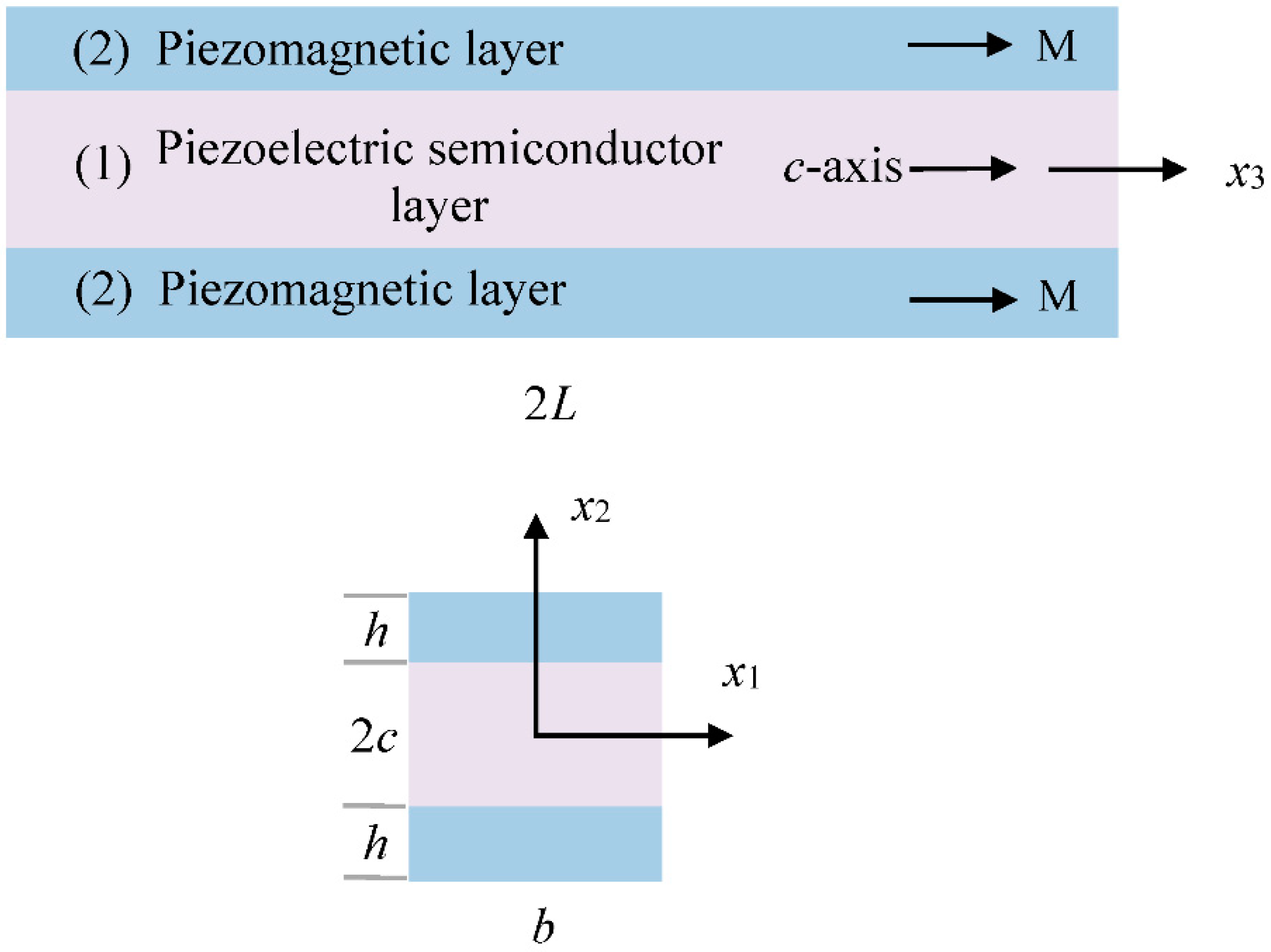
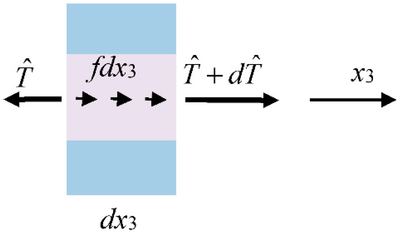
3. One-Dimensional Model for Extension

The equations in the previous section present considerable mathematical challenges. We consider thin rods and make a few approximations to simplify the problem. We assume that the following is approximately true throughout the composite rod during extension:
u 3 = u u ( x 3 , t ) , φ φ ( x 3 , t ) , ψ ψ ( x 3 , t ) ,
which are understood to be averages of the corresponding three-dimensional fields over the cross-section of the rod. Then
S 33 = u x 3 , E 3 = φ x 3 , H 3 = ψ x 3 .
Consider the piezoelectric semiconductor layer first. We perform the stress relaxation for thin rods (T11 = T22 = 0) using the following relevant constitutive relations from Equation (6):
T 11 = c 11 ( 1 ) S 11 + c 12 ( 1 ) S 22 + c 13 ( 1 ) S 33 e 31 ( 1 ) E 3 = 0 , T 22 = c 12 ( 1 ) S 11 + c 11 ( 1 ) S 22 + c 13 ( 1 ) S 33 e 31 ( 1 ) E 3 = 0 ,
T 33 = c 13 ( 1 ) S 11 + c 13 ( 1 ) S 22 + c 33 ( 1 ) S 33 e 33 ( 3 ) E 3 , D 3 = e 31 ( 1 ) ( S 11 + S 22 ) + e 33 ( 1 ) S 33 + ε 33 ( 1 ) E 3 .
Solving Equation (19) for expressions of S11 and S22, and then substituting them into Equation (20), one obtains the following constitutive relations for the extension of the piezoelectric semiconductor layer:
T = c ( 1 ) S e ( 1 ) E , D = e ( 1 ) S + ε ( 1 ) E ,
where the relevant axial fields and the one-dimensional effective material constants are denoted by
S = S 33 , T = T 33 , E = E 3 , D = D 3 ,
c ( 1 ) = c 33 ( 1 ) 2 ( c 13 ( 1 ) ) 2 c 11 ( 1 ) + c 12 ( 1 ) , e ( 1 ) = e 33 ( 1 ) 2 c 13 ( 1 ) e 31 ( 1 ) c 11 ( 1 ) + c 12 ( 1 ) , ε ( 1 ) = ε 33 ( 1 ) + 2 ( e 31 ( 1 ) ) 2 c 11 ( 1 ) + c 12 ( 1 ) .
We also denote the axial magnetic fields and the relevant magnetic material constant by
B = B 3 , H = H 3 , μ ( 1 ) = μ 33 ( 1 ) .
Then,
B = μ ( 1 ) H .
In the thin piezoelectric semiconductor layer, we also make the following approximations:
Δ p Δ p ( x 3 , t ) , Δ n Δ n ( x 3 , t ) .
With Equations (16) and (26), the constitutive relations for the axial current densities in the piezoelectric semiconductor layer can be simplified as
J p q p 0 μ p E q D p ( Δ p ) x 3 , J n q n 0 μ n E + q D n ( Δ n ) x 3 ,
where
μ p = μ 33 p , D p = D 33 p , μ n = μ 33 n , D n = D 33 n .
Similarly, for the piezomagnetic layers, after the lateral stress relaxation, we have
T = c ( 2 ) S h ( 2 ) H , D = ε ( 2 ) E , B = h ( 2 ) S + μ ( 2 ) H ,
where
c ( 2 ) = c 33 ( 2 ) 2 ( c 13 ( 2 ) ) 2 c 11 ( 2 ) + c 12 ( 2 ) , h ( 2 ) = h 33 ( 2 ) 2 c 13 ( 2 ) h 31 ( 2 ) c 11 ( 2 ) + c 12 ( 2 ) , ε ( 2 ) = ε 33 ( 2 ) , μ ( 2 ) = μ 33 ( 2 ) + 2 ( h 31 ( 2 ) ) 2 c 11 ( 2 ) + c 12 ( 2 ) .
For the composite rod, the total axial force is calculated from the integration of T3 over the entire cross-section of the composite rod, which in this case takes the following form:
T ^ = T A ( 1 ) + T A ( 2 ) = ( c ( 1 ) S e ( 1 ) E ) A ( 1 ) + ( c ( 2 ) S h ( 2 ) H ) A ( 2 ) = ( c ( 1 ) A ( 1 ) + c ( 2 ) A ( 2 ) ) S e ( 1 ) A ( 1 ) E h ( 2 ) A ( 2 ) H = c ^ S e ^ E h ^ H ,
where
c ^ = c ( 1 ) A ( 1 ) + c ( 2 ) A ( 2 ) , e ^ = e ( 1 ) A ( 1 ) , h ^ = h ( 2 ) A ( 2 ) , A ( 1 ) = 2 b c , A ( 2 ) = 2 b h .
A ( 1 ) and A ( 2 ) are the cross-sectional areas of the piezoelectric semiconductor and piezomagnetic layers, respectively. Similarly, the total axial electric displacement and total axial magnetic induction over the cross-section of the composite rod are
D ^ = D A ( 1 ) + D A ( 2 ) = ( e ( 1 ) S + ε ( 1 ) E ) A ( 1 ) + ( ε ( 2 ) E ) A ( 2 ) = e ( 1 ) A ( 1 ) S + ( ε ( 1 ) A ( 1 ) + ε ( 2 ) A ( 2 ) ) E = e ^ S + ε ^ E ,
B ^ = B A ( 1 ) + B A ( 2 ) = ( μ ( 1 ) H ) A ( 1 ) + ( h ( 2 ) S + μ ( 2 ) H ) A ( 2 ) = h ( 2 ) A ( 2 ) S + ( μ ( 1 ) A ( 1 ) + μ ( 2 ) A ( 2 ) ) H = h ^ S + μ ^ H ,
where
ε ^ = ε ( 1 ) A ( 1 ) + ε ( 1 ) A ( 2 ) , μ ^ = μ ( 1 ) A ( 1 ) + μ ( 1 ) A ( 2 ) .
For extension, the equation of motion of the rod in the axial direction can be obtained by considering a differential element of the rod with length dx3 as shown in Figure 2, which leads to [39]
T ^ x 3 + f ( x 3 , t ) = 2 b ( ρ ( 1 ) c + ρ ( 2 ) h ) 2 u t 2 .
where f ( x 3 , t ) is the axial mechanical load per unit length of the rod. Similarly [39], the one-dimensional charge equation of electrostatics, the one-dimensional Gauss equation of the magnetic induction, and the one-dimensional conservation of holes and electrons of the composite rod are
D ^ x 3 = q ( Δ p Δ n ) A ( 1 ) ,
B ^ x 3 = 0 ,
q t ( Δ p ) = J p x 3 , q t ( Δ n ) = J n x 3 .
Substituting Equations (27), (31), (33), and (34) into Equations (36)–(39), along with the use of Equation (18), one obtains
c ^ 2 u x 3 2 + e ^ 2 φ x 3 2 + h ^ 2 ψ x 3 2 + f ( x 3 , t ) = 2 b ( ρ ( 1 ) c + ρ ( 2 ) h ) 2 u t 2 , e ^ 2 u x 3 2 ε ^ 2 φ x 3 2 = q ( Δ p Δ n ) A ( 1 ) , h ^ 2 u x 3 2 μ ^ 2 φ x 3 2 = 0 , p 0 μ p 2 φ x 3 2 + D p 2 Δ p x 3 2 = t ( Δ p ) , D n 2 Δ n x 3 2 n 0 μ n 2 φ x 3 2 = t ( Δ n ) .
This is a system of coupled linear partial differential equations for u, φ, ψ, Δ p , and Δ n .

4. Analytical Solution

Specifically, we investigate the static extension of a mechanically free (f = 0) and electrically isolated rod under a static axial magnetic field produced by a magnetic potential difference at the two ends of the rod. The rod is within |x3| < L. The boundary conditions are
T ^ ( ± L ) = 0 , D ^ ( ± L ) = 0 , ψ ( ± L ) = ± ψ 0 , J n ( ± L ) = 0 , J p ( ± L ) = 0 .
We are not considering carrier recombination and generation. Therefore, Δ p and Δ n must satisfy the following global charge conservation conditions:
L L Δ p d x 3 = 0 , L L Δ n d x 3 = 0 .
Only one of Equation (42) is independent. The other is implied by integrating Equation (37) between −L and L and using the boundary conditions on D ^ in Equation (41), which implies that
L L q ( Δ p Δ n ) d x 3 = 0 .
Since there are no boundary conditions prescribed directly on the mechanical displacement and electric potential, the mechanical displacement may have an arbitrary constant representing a rigid-body translation of the rod along x3. At the same time, the electric potential may have an arbitrary constant that does not make any difference in the electric field it produces. To determine the mechanical displacement and electric potential uniquely, we set
u 3 ( 0 ) = 0 , φ ( 0 ) = 0 .
The relevant component of the polarization vector and distributed effective polarization charge can be calculated from
P = P 3 = D 3 ε 0 E 3 , ρ P = P i , i = P 3 , 3 , D 3 = D ^ / A , A = A ( 1 ) + A ( 2 ) .
The problem is time-independent. Thus, the terms on the right side of Equation (40) vanishes. Equation (40) reduces to a system of linear ordinary differential equations with constant coefficients. The solution can be obtained in a straightforward manner. The results are
ψ = e ^ 2 h ^ 2 c ˜ c ^ ε ˜ μ ^ ψ 0 Δ sinh ( k x 3 ) + k cosh ( k L ) ψ 0 Δ x 3 ,
u = e ^ 2 h ^ c ˜ c ^ ε ˜ ψ 0 Δ sinh ( k x 3 ) h ^ k cosh ( k L ) c ^ ψ 0 Δ x 3 ,
S = e ^ 2 h ^ k c ˜ c ^ ε ˜ ψ 0 Δ cosh ( k x 3 ) h ^ k cosh ( k L ) c ^ ψ 0 Δ ,
φ = e ^ h ^ c ^ ε ˜ ψ 0 Δ sinh ( k x 3 ) ,
E = e ^ h ^ k c ^ ε ˜ ψ 0 Δ cosh ( k x 3 ) ,
D = e ^ h ^ k c ^ A ψ 0 Δ cosh ( k x 3 ) e ^ h ^ k cosh ( k L ) c ^ A ψ 0 Δ ,
P = ( ε ˜ ε 0 A ) e ^ h ^ k c ^ ε ˜ A ψ 0 Δ cosh ( k x 3 ) e ^ h ^ k cosh ( k L ) c ^ A ψ 0 Δ ,
ρ P = ( ε 0 A ε ˜ ) e ^ h ^ k 2 c ^ ε ˜ A ψ 0 Δ sinh ( k x 3 ) ,
Δ n = μ n n 0 D n e ^ h ^ c ^ ε ˜ ψ 0 Δ sinh ( k x 3 ) ,
Δ p = μ p p 0 D p e ^ h ^ c ^ ε ˜ ψ 0 Δ sinh ( k x 3 ) ,
where
k 2 = q A ( 1 ) ε ˜ ( μ p D p p 0 + μ n D n n 0 ) , ε ˜ = ε ^ + e ^ 2 c ˜ , c ˜ = c ^ + h ^ 2 μ ^ , Δ = k L cosh ( k L ) + e ^ 2 h ^ 2 c ˜ c ^ ε ˜ μ ^ sinh ( k L ) .

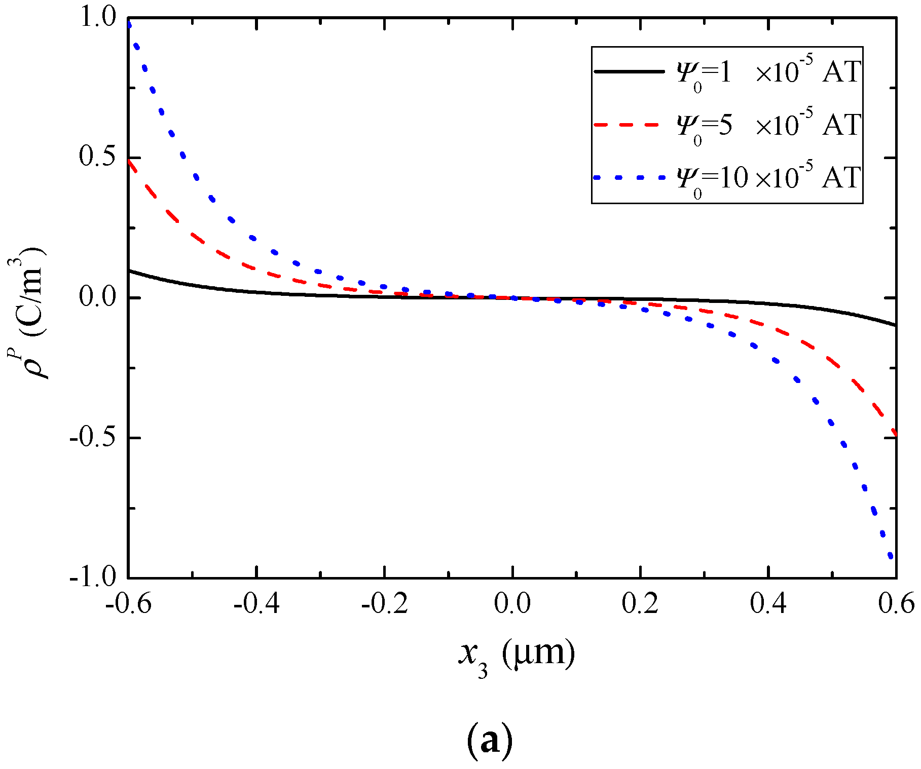
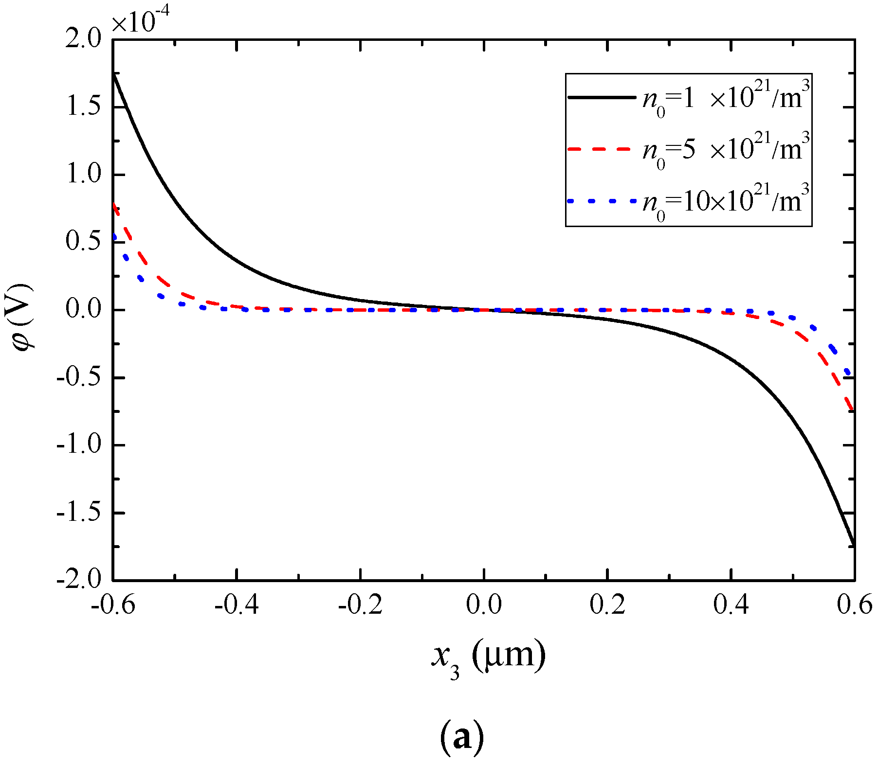
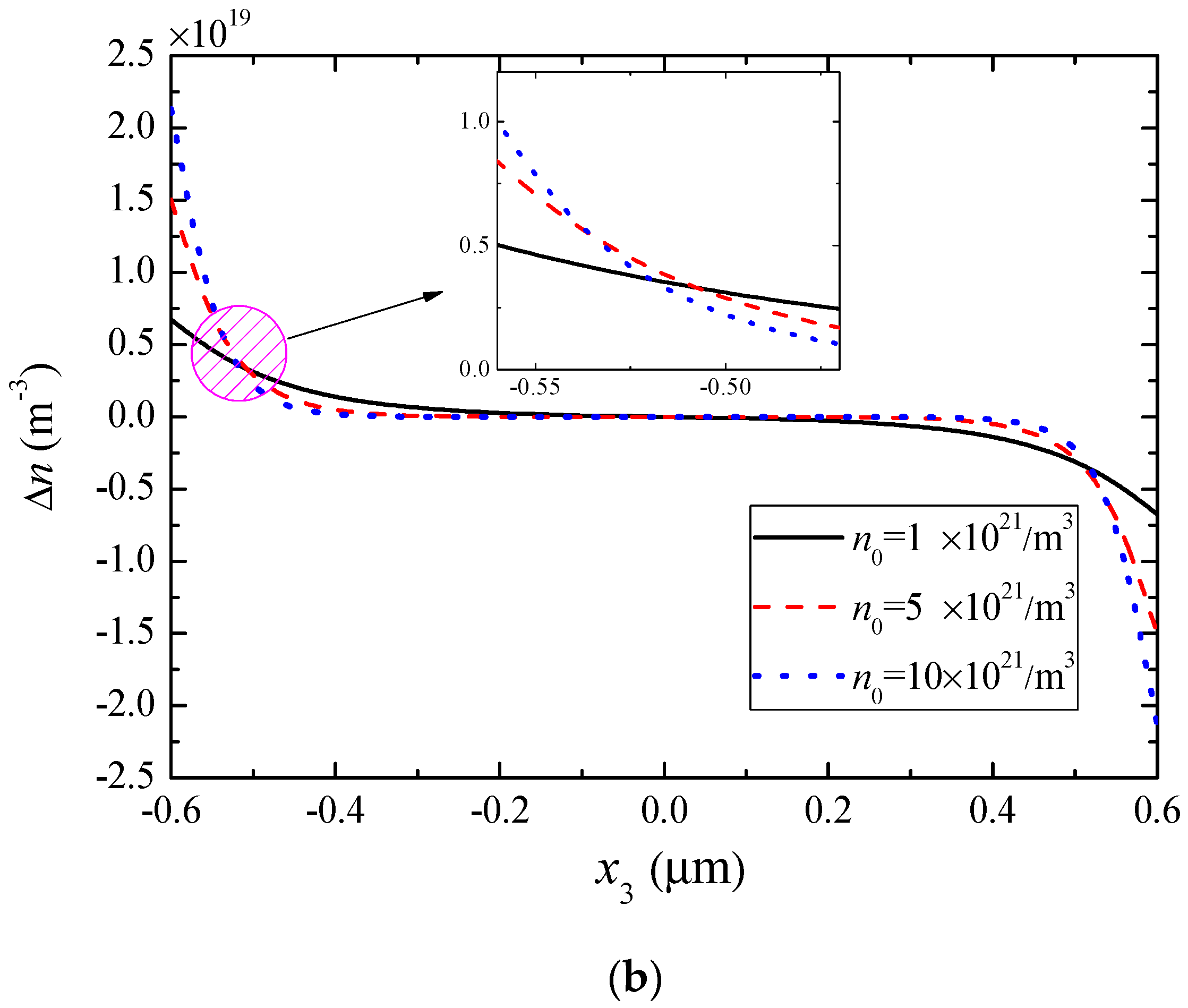
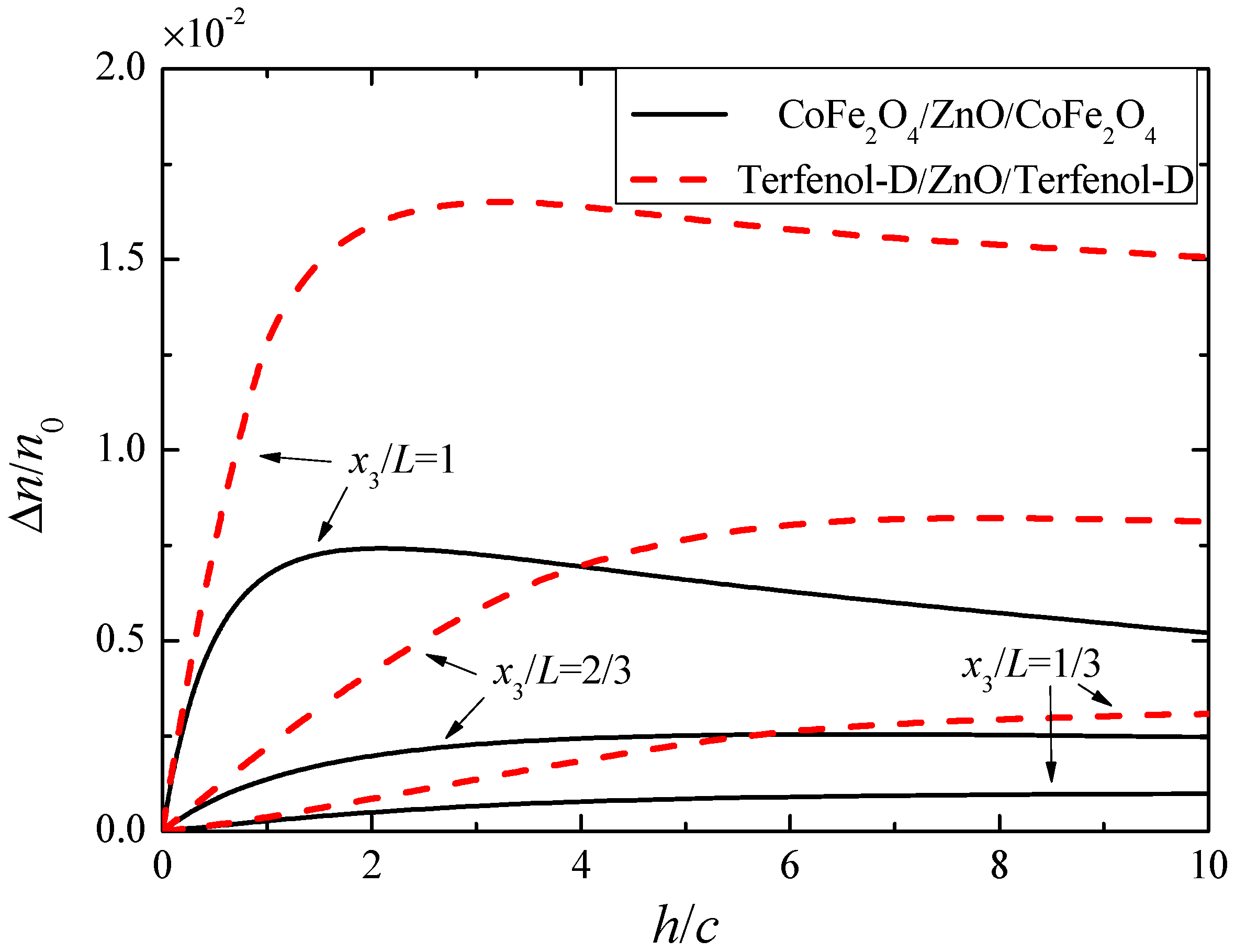
5. Numerical Results and Discussion

Based on the analytical solution in the previous section, the coupled fields are calculated and examined below. n-type ZnO is chosen as the piezoelectric semiconductor layer, while the two identical piezomagnetic layers are either CoFe2O4 or Terfenol-D. The relevant material properties are listed in Table 1.
We first examine the influence of the applied ψ0 and the initial carrier density on various fields. For the CoFe2O4/ZnO/CoFe2O4 composite rod with L = 0.6 µm, h = c =0.05 µm, and b = 0.2 µm, Figure 3 shows the axial distributions of the magnetic potential and piezomagnetically induced mechanical fields along the rod for different values of ψ0 when n 0 = 1 × 10 21 / m 3 . ψ is dominated by the applied ψ0 and is almost linear. To show the effect of couplings between ψ and other fields more clearly, in Figure 3a we plot Δ ψ = ψ ψ 0 x 3 / L instead of ψ itself. As ψ0 increases, all fields become stronger as expected. It is well known that in the special case when the piezoelectric layer in the middle is a dielectric without semiconduction, the magnetic potential and mechanical displacement in Figure 3b are both linear functions of x3 and, at the same time, the strain in Figure 3c is a constant. Because of semiconduction, all of these fields have hyperbolic behaviors as indicated by their expressions in Equations (46)–(48), especially near the ends of the rod where kL is relatively large.
Figure 4 shows the electric potential, electric field, and electric displacement produced by the extensional deformation through piezoelectric coupling. It can be seen from Figure 4 that the applied ψ0 has obvious influences on these electric variables. Again, they differ from the linear fields or constants in composite structures of piezoelectric and piezomagnetic dielectrics.
Our main interest is the development of the distributions of mobile charges in Figure 5b, which shows that the applied magnetic field causes redistribution of charge carriers through combined piezomagnetic/piezoelectric couplings and semiconduction. Figure 5a,b shows that the electrons redistribute themselves in such a way that they tend to screen the effective polarization charges. The applied ψ0 used is relatively small to insure that Δn is much smaller than n0, so that the assumption leading to the linearization in Equation (16) is not violated.
For the same composite rod, Figure 6, Figure 7 and Figure 8 show the effect of n0 on various fields when ψ 0 = 10 4 AT . Specifically, Figure 6 shows the magnetic potential and piezomagnetically induced mechanical fields. Figure 6b indicates that n0 has almost no influence on the mechanical displacement. From Figure 6a,c as well as Figure 7, it can be seen that the absolute values of Δψ, strain, and electric potential decrease monotonically with the increase of n0, but the electric filed and electric displacement increase monotonically. In addition, the effect of n0 on these fields is relatively small near the two ends and the middle of the rod. Figure 8 shows the variations of the effective polarization charge and electron concentration perturbation. They assume maximal values at the ends of the rod.
In order to reveal the dependence of the electron concentration perturbation on the material combinations and the thickness ratio h/c between the piezomagnetic layers and piezoelectric semiconductor layer, we rewrite Equation (54) as
Δ n n 0 = q k B T γ ψ 0 ,
where
γ = e ^ h ^ c ^ ε ˜ Δ sinh ( k x 3 ) .
In Equation (57), the following Einstein relation has been used:
μ n D n = μ p D p = q k B T ,
where T is the absolute temperature and kB is the Boltzmann constant. γ describes the strength of the coupling effect of interest, i.e., the development of carrier redistribution under a magnetic field. For a given cross-section location, γ depends on the relevant material constants and the thickness ratio h/c. It also varies with x3. Figure 9 shows the variation of γ with h/c for two material combinations, i.e., CoFe2O4/ZnO/CoFe2O4 and Terfenol-D/ZnO/Terfenol-D while h + c is held constant. It can be seen that for the CoFe2O4/ZnO/CoFe2O4 rod, γ is always less than that for Terfenol-D/ZnO/Terfenol-D rod. At the ends of the rod, γ has a maximum for a certain value of h/c. This is as expected because either the piezoelectric semiconductor layer or piezomagnetic layers cannot be too thin. Otherwise, there will be insufficient mobile charges or insufficient piezomagnetically induced deformation. Both the exact value of h/c for the maximal γ and the value of the maximal γ are sensitive to the component materials. Compared with Terfenol-D, CoFe2O4 has a larger h33, which increases γ according to Equation (58), but CoFe2O4 has a much larger c33, which lowers γ. The net result of these two competing effects is that the Terfenol-D/ZnO/Terfenol-D rod has a significantly larger γ than the CoFe2O4/ZnO/CoFe2O4 rod.

6. Conclusions

We have shown theoretically that in a properly constructed composite rod of piezoelectric semiconductors and piezomagnetics, an applied axial magnetic field produces a series of fields, including extensional deformation through the piezomagnetic coupling, polarization through the piezoelectric coupling, and redistribution of mobile charges because of semiconduction. The rod may be potentially used as a magnetic field sensor or magnetic field-to-current transducer. The material combination and thickness ratio between the piezomagnetic layer and piezoelectric semiconductor layer has strong influences on the strength of the coupling between the applied magnetic field and carrier redistribution. For a given material combination, there exists an optimal thickness ratio at which the coupling is the strongest. Hence, the redistribution or motion of mobile charges in the composite rod can be modulated by the applied magnetic field with proper design of the structure through materials and geometry.

Author Contributions

G.W. derived the solution of the considered problem, computed the numerical results and plotted all figures; J.L. checked the correctness of the obtained solution and numerical computation, approved the final version to be published; W.F. examined and analyzed the reasonability of the numerical results; J.Y. presented the idea of this work, established the analytical model and drafted the work. All authors have read and agreed to the published version of the manuscript.

Funding

This work was supported by the National Natural Science Foundation of China (Grant No. 11472182).

Conflicts of Interest

The authors declare no conflict of interest.

References

  1. Hickernell, F.S. The piezoelectric semiconductor and acoustoelectronic device development in the sixties. IEEE Trans. Ultrason. Ferroelectr. Freq. Control 2005, 52, 737–745. [Google Scholar] [CrossRef] [PubMed]
  2. Wang, Z.L.; Wu, W.Z.; Falconi, C. Piezotronics and piezo-phototronics with third-generation semiconductors. MRS Bull. 2018, 43, 922–927. [Google Scholar] [CrossRef] [Green Version]
  3. Zhang, Y.; Leng, Y.S.; Willatzen, M.; Huang, B.L. Theory of piezotronics and piezo-phototronics. MRS Bull. 2018, 43, 928–935. [Google Scholar] [CrossRef]
  4. Hu, W.G.; Kalantar-Zadeh, K.; Gupta, K.; Liu, C.P. Piezotronic materials and large-scale piezotronics array devices. MRS Bull. 2018, 43, 936–940. [Google Scholar] [CrossRef]
  5. Fröemling, T.; Yu, R.M.; Mintken, M.; Adelung, R.; Rödel, J. Piezotronic sensors. MRS Bull. 2018, 43, 941–945. [Google Scholar] [CrossRef]
  6. Wang, X.D.; Rohrer, G.S.; Li, H.X. Piezotronic modulations in electro- and photochemical catalysis. MRS Bull. 2018, 43, 946–951. [Google Scholar] [CrossRef]
  7. Bao, R.R.; Hu, Y.F.; Yang, Q.; Pan, C.F. Piezophototronic effect on optoelectronic nanodevices. MRS Bull. 2018, 43, 952–958. [Google Scholar] [CrossRef]
  8. Gao, P.X.; Song, J.H.; Liu, J.; Wang, Z.L. Nanowire piezoelectric nanogenerators on plastic substrates as flexible power sources for nanodevices. Adv. Mater. 2007, 19, 67–72. [Google Scholar] [CrossRef]
  9. Romano, G.; Mantini, G.; Garlo, A.D.; D’Amico, A.; Falconi, C.; Wang, Z.L. Piezoelectric potential in vertically aligned nanowires for high output nanogenerators. Nanotechnology 2011, 22, 465401. [Google Scholar] [CrossRef]
  10. Liu, Y.D.; Wahyudin, E.T.N.; He, J.H.; Zhai, J.Y. Piezotronics and piezo-phototronics in two-dimensional materials. MRS Bull. 2018, 43, 959–964. [Google Scholar] [CrossRef] [Green Version]
  11. Cui, N.Y.; Wu, W.W.; Zhao, Y.; Bai, S.; Meng, L.X.; Qin, Y.; Wang, Z.L. Magnetic force driven nanogenerators as a noncontact energy harvester and sensor. Nano Lett. 2012, 12, 37013705. [Google Scholar] [CrossRef]
  12. Huang, L.B.; Bai, G.X.; Wong, M.C.; Yang, Z.B.; Wu, W.; Hao, J.H. Magnetic-assisted noncontact triboelectric nanogenerator converting mechanical energy into electricity and light emissions. Adv. Mater. 2016, 28, 2744–2751. [Google Scholar] [CrossRef] [PubMed]
  13. Wong, M.C.; Chen, L.; Tsang, M.K.; Zhang, Y.; Hao, J.H. Magnetic-induced luminescence from flexible composite laminates by coupling magnetic field to piezophotonic effect. Adv. Mater. 2015, 27, 4488–4495. [Google Scholar] [CrossRef] [PubMed]
  14. Peng, M.Z.; Zhang, Y.; Liu, Y.D.; Song, M.; Zhai, J.Y.; Wang, Z.L. Magnetic-mechanical-electrical-optical coupling effects in GaN-based led/rare-earth Terfenol-D structures. Adv. Mater. 2014, 26, 6767–6772. [Google Scholar] [CrossRef]
  15. Liu, Y.D.; Guo, J.M.; Yu, A.F.; Zhang, Y.; Kou, J.Z.; Zhang, K.; Wen, R.M.; Zhang, Y.; Zhai, J.Y.; Wang, Z.L. Magnetic-induced-piezopotential gated MoS2 field-effect transistor at room temperature. Adv. Mater. 2018, 30, 1704524. [Google Scholar] [CrossRef] [PubMed]
  16. Piotrowski, C.; Bendson, S.A.; Loeding, N.W.; Mularie, W.M. Integrated Magnetostrictive-Piezoelectric-Metal Oxide Semiconductor Magnetic Playback Head. U.S. Patent 4,520,413, 28 May 1985. [Google Scholar]
  17. Srinivasan, G.; Laletsin, V.M.; Hayes, R.; Puddubnaya, N.; Rasmussen, E.T.; Fekel, D.J. Giant magnetoelectric effects in layered composites of nickel zinc ferrite and lead zirconate titanate. Solid State Commun. 2002, 124, 373–378. [Google Scholar] [CrossRef]
  18. Bichurin, M.I.; Petrov, V.M.; Srinivasan, G. Theroy of low frequency magnetoelectric effects in ferromagnetic-ferroelectric layered composites. J. Appl. Phys. 2002, 92, 7681–7683. [Google Scholar] [CrossRef]
  19. Dong, S.X.; Li, J.F.; Viehlan, D. Giant magneto-electric effect in laminate composites. IEEE Trans. Ultrason. Ferroelectr. Freq. Control 2003, 50, 1236–1239. [Google Scholar] [CrossRef]
  20. Soh, A.K.; Liu, J.X. Interfacial shear horizontal waves in a piezoelectric-piezomagnetic bi-material. Phil. Mag. Lett. 2006, 86, 31–35. [Google Scholar] [CrossRef]
  21. Chen, W.Q.; Lee, K.Y.; Ding, H.J. On free vibration of non-homogeneous transversely isotropic magneto-electro-elastic plates. J. Sound Vib. 2005, 279, 237–251. [Google Scholar] [CrossRef]
  22. Nan, C.W.; Bichurin, M.I.; Dong, S.X.; Viehland, D.; Srinivasan, G. Multiferroic magnetoelectric composites: Historical perspectives, status, and future directions. J. Appl. Phys. 2008, 103, 031101. [Google Scholar] [CrossRef]
  23. Auld, B.A. Acoustic Fields and Waves in Solids; John Wiley and Sons: New York, NY, USA, 1973; Volume I. [Google Scholar]
  24. Pierret, R.F. Semiconductor Device Fundamentals; Pearson: Uttar Pradesh, India, 1996. [Google Scholar]
  25. Wauer, J.; Suherman, S. Thickness vibrations of a piezo-semiconducting plate layer. Int. J. Eng. Sci. 1997, 35, 1387–1404. [Google Scholar] [CrossRef]
  26. Li, P.; Jin, F.; Yang, J.S. Effects of semiconduction on electromechanical energy conversion in piezoelectrics. Smart Mater. Struct. 2015, 24, 025021. [Google Scholar] [CrossRef]
  27. Gu, C.L.; Jin, F. Shear-horizontal surface waves in a half-space of piezoelectric semiconductors. Phil. Mag. Lett. 2015, 95, 92–100. [Google Scholar] [CrossRef]
  28. Sharma, J.N.; Sharma, K.K.; Kumar, A. Acousto-diffusive waves in a piezoelectric-semiconductor-piezoelectric sandwich structure. World J. Mech. 2011, 1, 247–255. [Google Scholar] [CrossRef] [Green Version]
  29. Jiao, F.Y.; Wei, P.J.; Zhou, Y.H.; Zhou, X.L. Wave propagation through a piezoelectric semiconductor slab sandwiched by two piezoelectric half-spaces. Eur. J. Mech. A-Solids 2019, 75, 70–81. [Google Scholar] [CrossRef]
  30. Jiao, F.Y.; Wei, P.J.; Zhou, Y.H.; Zhou, X.L. The dispersion and attenuation of the multi-physical fields coupled waves in a piezoelectric semiconductor. Ultrasonics 2019, 92, 68–78. [Google Scholar] [CrossRef]
  31. Liang, Y.X.; Hu, Y.T. Effect of interaction among the three time scales on the propagation characteristics of coupled waves in a piezoelectric semiconductor rod. Nano Energy 2019, 68, 104345. [Google Scholar] [CrossRef]
  32. Tian, R.; Liu, J.X.; Pan, E.; Wang, Y.S.; Soh, A.K. Some characteristics of elastic waves in a piezoelectric semiconductor plate. J. Appl. Phys. 2019, 126, 125701. [Google Scholar] [CrossRef]
  33. Sladek, J.; Sladek, V.; Pan, E.; Wuensche, M. Fracture analysis in piezoelectric semiconductors under a thermal load. Eng. Fract. Mech. 2014, 126, 27–39. [Google Scholar] [CrossRef]
  34. Zhao, M.H.; Pan, Y.B.; Fan, C.Y.; Xu, G.T. Extended displacement discontinuity method for analysis of cracks in 2D piezoelectric semiconductors. Int. J. Solids Struct. 2016, 94–95, 50–59. [Google Scholar] [CrossRef]
  35. Qin, G.S.; Lu, C.S.; Zhang, X.; Zhao, M.H. Electric current dependent fracture in GaN piezoelectric semiconductor ceramics. Materials 2018, 11, 2000. [Google Scholar] [CrossRef] [PubMed] [Green Version]
  36. Zhang, C.L.; Luo, Y.X.; Cheng, R.R.; Wang, X.Y. Electromechanical fields in piezoelectric semiconductor nanofibers under an axial force. MRS Adv. 2017, 2, 3421–3426. [Google Scholar] [CrossRef] [Green Version]
  37. Afraneo, R.; Lovat, G.; Burghignoli, P.; Falconi, C. Piezo-semiconductive quasi-1D nanodevices with or without anti-symmetry. Adv. Mater. 2012, 24, 4719–4724. [Google Scholar] [CrossRef]
  38. Zhao, M.H.; Liu, X.; Fan, C.Y.; Lu, C.S.; Wang, B.B. Theoretical analysis on the extension of a piezoelectric semi-conductor nanowire: Effects of flexoelectricity and strain gradient. J. Appl. Phys. 2020, 127, 085707. [Google Scholar] [CrossRef]
  39. Cheng, R.R.; Zhang, C.L.; Chen, W.Q.; Yang, J.S. Piezotronic effects in the extension of a composite fiber of piezoelectric dielectrics and nonpiezoelectric semiconductors. J. Appl. Phys. 2018, 124, 064506. [Google Scholar] [CrossRef]
  40. Gao, Y.F.; Wang, Z.L. Electrostatic potential in a bent piezoelectric nanowire. The fundamental theory of nanogenerator and nanopiezotrionics. Nano Lett. 2007, 7, 2499–2505. [Google Scholar] [CrossRef]
  41. Gao, Y.F.; Wang, Z.L. Equilibrium potential of free charge carriers in a bent piezoelectric semiconductive nanowire. Nano Lett. 2009, 9, 1103–1110. [Google Scholar] [CrossRef]
  42. Fan, S.Q.; Liang, Y.X.; Xie, J.M.; Hu, Y.T. Exact solutions to the electromechanical quantities inside a statically-bent circular ZnO nanowire by taking into account both the piezoelectric property and the semiconducting performance: Part I-Linearized analysis. Nano Energy 2017, 40, 82–87. [Google Scholar] [CrossRef]
  43. Liang, Y.X.; Fan, S.Q.; Chen, X.D.; Hu, Y.T. Nonlinear effect of carrier drift on the performance of an n-type ZnO nanowire nanogenerator by coupling piezoelectric effect and semiconduction. Nanotechnology 2018, 9, 1917–1925. [Google Scholar] [CrossRef]
  44. Dai, X.Y.; Zhu, F.; Qian, Z.H.; Yang, J.S. Electric potential and carrier distribution in a piezoelectric semiconductor nanowire in time-harmonic bending vibration. Nano Energy 2018, 43, 22–28. [Google Scholar] [CrossRef]
  45. Liang, Y.X.; Hu, Y.T. Influence of doping concentration on the outputs of a bent ZnO nanowire. IEEE Trans. Ultrason. Ferroelectr. Freq. Control 2019, 66, 1793–1797. [Google Scholar] [CrossRef] [PubMed]
  46. Luo, Y.X.; Zhang, C.L.; Chen, W.Q.; Yang, J.S. An analysis of PN junctions in piezoelectric semiconductors. J. Appl. Phys. 2017, 122, 204502. [Google Scholar] [CrossRef]
  47. Yang, G.Y.; Du, J.K.; Wang, J.; Yang, J.S. Electromechanical fields in a nonuniform piezoelectric semiconductor rod. Mech. Mater. Struct. 2018, 13, 103–120. [Google Scholar] [CrossRef]
  48. Luo, Y.X.; Cheng, R.R.; Zhang, C.L.; Chen, W.Q.; Yang, J.S. Electromechanical fields near a circular PN Junction between two piezoelectric semiconductors. Acta Mech. Solida Sin. 2018, 31, 127–140. [Google Scholar] [CrossRef]
  49. Guo, M.K.; Li, Y.; Qin, G.S.; Zhao, M.H. Nonlinear solutions of PN junctions of piezoelectric semiconductors. Acta Mech. 2019, 230, 1825–1841. [Google Scholar] [CrossRef]
  50. Qin, L.F.; Chen, Q.M.; Cheng, H.B.; Chen, Q.; Li, J.F.; Wang, Q.M. Viscosity sensor using ZnO and AlN thin film bulk acoustic resonators with tilted polar c-axis orientations. J. Appl. Phys. 2011, 110, 094511. [Google Scholar] [CrossRef]
  51. Srinivas, S.; Li, J.Y.; Zhou, Y.C.; Soh, A.K. The effective magnetoelectroelastic moduli of matrix-based multiferroic composites. J. Appl. Phys. 2006, 99, 043905. [Google Scholar] [CrossRef] [Green Version]
  52. Pan, E.; Chen, W.Q. Green’s Functions in Anisotropic Media; Cambridge University Press: New York, NY, USA, 2015. [Google Scholar]
Figure 1. A composite rod of a piezoelectric semiconductor and piezomagnetics.
Materials 13 03115 g001
Figure 2. A differential element of the composite rod under mechanical loads.
Materials 13 03115 g002
Figure 3. Magnetic potential and piezomagnetically induced mechanical fields under different ψ 0 when n 0 = 1 × 10 21 / m 3 . (a) Δ ψ = ψ ψ 0 x 3 / L , (b) mechanical displacement, (c) strain.
Materials 13 03115 g003aMaterials 13 03115 g003b
Figure 4. Piezoelectrically induced electric fields under different ψ 0 when n 0 = 1 × 10 21 / m 3 . (a) Electric potential, (b) electric field, (c) electric displacement.
Materials 13 03115 g004aMaterials 13 03115 g004b
Figure 5. Polarization-induced charge distributions under different ψ 0 when n 0 = 1 × 10 21 / m 3 . (a) Effective polarization charge and (b) electron concentration perturbation.
Materials 13 03115 g005aMaterials 13 03115 g005b
Figure 6. Magnetic potential and piezomagnetically induced mechanical fields for different n0 when ψ 0 = 10 4 AT . (a) Δ ψ = ψ ψ 0 x 3 / L , (b) mechanical displacement, (c) strain.
Materials 13 03115 g006aMaterials 13 03115 g006b
Figure 7. Piezoelectrically induced electric fields for different n0 when ψ 0 = 10 4 AT . (a) Electric potential, (b) electric field, (c) electric displacement.
Materials 13 03115 g007aMaterials 13 03115 g007b
Figure 8. Polarization-induced charge distributions for different n0 when ψ 0 = 10 4 AT . (a) Effective polarization charge, (b) electron concentration perturbation.
Materials 13 03115 g008aMaterials 13 03115 g008b
Figure 9. Δ n / n 0 versus h/c at different locations along the rod.
Materials 13 03115 g009
Table 1. Material properties of ZnO [50], CoFe2O4 [51], and Terfenol-D [52].
ZnOCoFe2O4Terfenol-D
c11(GPa)2102868.541
c12(GPa)1211730.654
c13(GPa)105170.53.91
c33(GPa)211269.528.3
e31(C/m2)−0.5700
e33(C/m2)1.3200
ε33(10−11F/m)8.859.35
h31(m/A)0580.3−5.75
h33(m/A)0699.7270.1
μ33(10−6Ns2/C2)101572.3

