Article

Optical Characterization of AsxTe100−x Films Grown by Plasma Deposition Based on the Advanced Optimizing Envelope Method

1
College of Energy and Electronics, Technical University of Sofia, 2140 Botevgrad, Bulgaria
2
Department of Microelectronics, Technical University of Sofia, 1000 Sofia, Bulgaria
3
Laboratory of Functional Nanomaterials, Lobachevsky University, 603950 Nizhny Novgorod, Russia
*
Authors to whom correspondence should be addressed.
Materials 2020, 13(13), 2981; https://doi.org/10.3390/ma13132981
Submission received: 9 June 2020 / Revised: 24 June 2020 / Accepted: 27 June 2020 / Published: 3 July 2020

Abstract

:
Three AsxTe100x films with different x and dissimilar average thickness d ¯ are characterized mainly from one interference transmittance spectrum T(λ = 300 to 3000 nm) of such film on a substrate based on the advanced optimizing envelope method (AOEM). A simple dual transformation of T(λ) is proposed and used for increasing the accuracy of computation of its envelopes T+(λ) and T(λ) accounting for the significant glass substrate absorption especially for λ > 2500 nm. The refractive index n(λ) of As40Te60 and As98Te2 films is determined with a relative error <0.30%. As far as we know, the As80Te20 film is the only one with anomalous dispersion and the thickest, with estimated d ¯ = 1.1446 nm, ever characterized by an envelope method. It is also shown and explained why the extinction coefficient k(λ) of any of the three AsxTe100x films is computed more accurately from the quantity Ti(λ) = [T+(λ)T(λ)]0.5 compared to its commonly employed computation from T+(λ). The obtained results strengthen our conviction that the AOEM has a capacity for providing most accurate optical characterization of almost every dielectric or semiconductor film with d ¯ > 300 nm on a substrate, compared to all the other methods for characterization of such films only from T(λ).

1. Introduction

Thin films have widespread applications in optics, optoelectronics and magneto-optics [1,2], as the films can be deposited by different techniques, using various technology regimes [3,4,5]. The ever increasing requirements regarding the performance of devices containing such films determine the necessity for increasing the accuracy of optical characterization of the films.
Most optical methods for characterization of thin films use at least one normal incidence transmittance spectrum T(λ) of a specimen consisting of the studied film deposited on a light transmitting substrate, such as glass [6,7]. Such methods can be classified into three groups: dispersion methods, hybrid methods, and interference methods [8]. The dispersion methods, including all spectroscopic ellipsometry methods, implement a dispersion model represented by a formula containing at least one of the components of the complex refractive index [9,10]. However, dispersion models are usually not accurate for doped films [11,12], organic films [13,14], and mechanically stressed films [15]. In the hybrid methods, a dispersion model or independent measurement of the film thickness is used, which is often insufficiently accurate, together with T(λ) [13,16].
The interference methods employ at least one interference transmittance or reflectance spectrum, i.e., a spectrum containing interference pattern with several maxima and minima due to light interference in the film [17,18]. The most popular interference method is the founding envelope method (FEM) of Swanepoel [19], which employs only one normal incidence transmittance spectrum T(λ) of the specimen, and is the most cited method for optical characterization of a thin film, with over 4400 citations [20]. The FEM also uses a computed smoothed spectrum Tsm(λ) of T(λ), as well as its upper envelope T+(λ) and lower envelope T(λ). Notwithstanding its popularity, the FEM from [19] and its modifications [21,22,23,24,25,26] assume that the film has uniform thickness d ¯ and the substrate is transparent, which can result in significant errors in film characterization. Both the thickness non-uniformity ∆d ≥ 0 of the film over the light spot and the substrate absorption have been taken into account in the improved envelope method (IEM) [27]. However, it uses three subjectively chosen parameters which can also lead to significant film characterization errors.
The optimizing envelope method (OEM) [28] determines optimized values of the above mentioned three parameters, and employs them in the computation of d ¯ , ∆d, and the spectral dependencies of the refractive index n(λ) and the extinction coefficient k(λ) of the film illustrated in Figure 1.
The smoothed normal incidence transmittance spectrum Tsm (λ) of the specimen from Figure 1 was formulated in [28] as:
T sm ( λ ) = 1 φ 2 φ 1 φ 1 φ 2 T u ( φ ) d φ = ( τ a , f τ f , s τ s , a ) 2 x s φ 2 φ 1 φ 1 φ 2 x d φ a 1 b 1 cos ( φ ) + c 1 sin ( φ ) ,
where:
φ = 4 π n d / λ , φ 1 = 4 π n ( d ¯ Δ d ) / λ , φ 2 = 4 π n ( d ¯ + Δ d ) / λ , x = exp ( 4 π k d / λ ) , x s = exp ( 4 π k s d s / λ ) , a 1 = 1 ( ρ a , f ρ s , a x x s ) 2 + ρ f , s 2 ( ρ a , f 2 x 2 ρ s , a 2 x s 2 ) ,
b 1 = 2 ρ a , f ρ f , s ρ s , a x [ ρ s , a x s 2 cos Δ 2 ρ s , a 1 cos Δ 1 ] , c 1 = 2 ρ a , f ρ f , s ρ s , a x [ ρ s , a x s 2 sin Δ 2 ρ s , a 1 sin Δ 1 ] ,
τ a , f τ f , s τ s , a = 8 ( n + 1 ) 2 + k 2 n 2 + k 2 ( n + n s ) 2 + ( k + k s ) 2 n s 2 + k s 2 ( n s + 1 ) 2 + k s 2 ,
ρ a , f = ( n 1 ) 2 + k 2 ( n + 1 ) 2 + k 2 , ρ f , s = ( n n s ) 2 + ( k k s ) 2 ( n + n s ) 2 + ( k + k s ) 2 , ρ s , a = ( n s 1 ) 2 + k s 2 ( n s + 1 ) 2 + k s 2 ,
Δ 1 = tan 1 ( 2 k n 2 + k 2 1 ) + π + tan 1 [ 2 ( k n s k s n ) n 2 n s 2 + k 2 k s 2 ] , Δ 2 = tan 1 ( 2 k n 2 + k 2 1 ) + π tan 1 [ 2 ( k n s k s n ) n 2 n s 2 + k 2 k s 2 ] ;
where Tu(λ) represents the transmittance of a uniform film on the same substrate, x(λ) is the absorbance of the film, and the subscript ‘s’ refers to the respective known substrate characteristics. It is assumed in Equation (1) that the film thickness d has a continuous uniform distribution in the interval ( d ¯ − ∆d, d ¯ + ∆d) over the light spot on the film surface, as the light passing through the film is considered to be coherent.
In an advanced version of the OEM (AOEM) [29] was pointed out that partial coherence of light, due to both light scattering from the film and finite slit width, results in slight shrinkage of the interference pattern. To offset these effects, it was proposed in [29] that the smoothed spectrum Tsm(λ) should be computed by “external smoothing” of T(λ), to correspond to the coherence of light passing through the film assumed in Equation (1), instead of the commonly used “internal smoothing” of T(λ).
The envelopes T+(λ) and T(λ) of Tsm(λ) were computed in [29] by combining the advantages of including extra points for the interpolation of both envelopes [30], with these of using iterations [31], however, implying substrate transparency for all λ. Moreover, points T+(λt) and T(λt) were adjusted in the spectral region with xs(λ) < 1 to take into account the substrate non-transparency there [29]. The following accurate formula for the envelope T+(λ) was also presented in [29]:
T + ( λ ) = 1 φ 2 + φ 1 + φ 1 + φ 2 + T u ( φ + ) d φ + = ( τ a , f τ f , s τ s , a ) 2 x s φ 2 + φ 1 + φ 1 + φ 2 + x d φ + a 1 b 1 cos ( φ + ) + c 1 sin ( φ + ) ,
where φ + = 4 π n ( d d ¯ ) / λ , φ 1 + = 4 π n Δ d / λ , φ 2 + = 4 π n Δ d / λ . Equations (1) and (2) have been derived assuming n2(λ) > ns2(λ) >> k2(λ) and ns2(λ) >> ks2(λ) [27], as these relationships are usually satisfied in the UV/VIS/NIR spectral region for a thin dielectric or semiconductor film with d ¯ = (300,5000) nm on a glass substrate [24].
Main advantage of the envelope methods (EM) is that they do not employ and dispersion model, as a result of using the interference fringes equation [19,21,22,23,24,25,26,27,28,29]:
2 n ( λ t ) d ¯ = m i ( λ t ) λ t ( i ) { m i 1 integer   for   all   tangency   wavelengths   λ t +   from   the   envelope   T + ( λ ) m i 1 / 2 half integer   for   all   tangency   wavelengths   λ t   from   the   envelope   T ( λ ) .
The tangency wavelengths λt(i) in Equation (3) represent the tangency points Tsm(λt) between Tsm(λ) and its two envelopes, where ‘i’ is a positive integer showing the number of the ‘i-th’ extremum of Tsm(λ) counted from 1 closest from the higher wavelengths end, and mi(λt) is the interference order.
The AOEM is executed in two stages, as at the end of its first stage are computed both the average thickness d ¯ , and the thickness non-uniformity ∆d ≥ 0 of the film over the light spot, as well as the first interference order m1(max(λt)) [28,29]. This is achieved by minimization of an error metric. The performance of seven possible error metrics was compared in [32], as it was shown there that using the AOEM and the error metric:
1 N i = 1 N { d ¯ d ¯ 0 [ λ t ( i ) ] } 2 N = δ d N 0
which provides d ¯ with an accuracy of 0.06% independent from the characteristics of model homogeneous films. In Equation (4), d ¯ 0(λt(i)) are estimated values of d ¯ , N is an optimized number of adjacent tangency wavelengths λt(i) participating in the computations, and δd is the root mean square deviation of d ¯ 0(λt(i)) from d ¯ . The employment of larger optimized N in Equation (4) and more accurate respective values of d ¯ and m1 make possible accurate characterization of thicker films by the AOEM in comparison with the FEM and the IEM [5,29].
In the second stage of the AOEM the refractive index n(λ) of the film is computed by optimized curve fitting over approximated values n0{Λt} of n{Λt} calculated by using Equation (3), where the wavelengths set {Λt} contains all wavelengths used in the interpolation of the envelopes of Tsm(λ), including all λt [29]. The extinction coefficient k(λ) of the film can be determined as:
k [ T sm ( λ ) ] = k 0 ( λ ) + Δ k ( λ )
where k0(λ) is its coherent light approximation computed by optimized curve fitting over its approximated values kc{Λt} computed from Tsm(λ) by solving Equation (1), and Δk(λ) ≥ 0 is a partially coherent light correction [29]. However, k(λ) has been most often computed from T+(λ) [27,33], e.g., by solving Equation (2) using numerical integration.
The following fitting functions Ff were used for deriving the optimized curve fitted n(λ) and k0(λ) in [29]:
{ 1 ) . For   fitting   n ( λ ) : F f = Polynomial   of   optimized   degree   p o N f 1 providing   min [ F r ( p ) / ( N f 1 p ) ] , where : N f 1 is   the   number   of   tangency   wavelengths   λ t ,   p is   the   polynomial   degree , F r ( p ) is   the   sum   of   the   square   of   the   residuals   over   the   set { Λ f } for   the   polynomial of   degree   p , e . g . F r ( n { Λ f } , p ) = f = 1 N f [ F f ( n { Λ f } ) n 0 { Λ f } ] 2 ; 2 ) . For   fitting   k 0 ( λ ) : F f = Two terms   exponential = u 1 exp ( u 2 λ ) + u 3 exp ( u 4 λ ) , where   u 1 , u 2 , u 3 , u 4 are   adjustable   parameters .
The Ffs from Equation (6) were suitable enough and contained sufficient number of parameters, providing smooth dependencies n(λ) and k0(λ) for the thin films characterized in [29] by the AOEM.
After a given thin film characterization is completed, its quality can be assessed by computation of a reconstructed transmittance spectrum Tr(λ), setting all characterization results in the right side of Equation (1), and its comparison with T(λ). A measure of the resemblance of Tr(λ) to T(λ) is the figure of merit:
F O M = j = 1 N j { T [ λ ( j ) ] T r [ λ ( j ) ] } 2 N j 0
with summation over all λ⊂[min(λt),λt(1)], as smaller FOM corresponds to more accurate film characterization.
Based on using FOM from Equation (7), it was shown in [28] that the OEM provides more accurate film characterization compared to the FEM and the IEM, for all specimens studied there. Furthermore, FOMs were compared in [34] for characterizations of sputtered a-Si thin films with dissimilar average thicknesses by the OEM, the optimizing graphical method (OGM) [35], the Tauc–Lorentz–Urbach model method (TLUM) [36], and the Cody–Lorentz–Urbach model method (CLUM) [37]. These four film characterization methods were selected as most likely to provide accurate characterization of the a-Si films. The results from [34] showed that the OEM provided most accurate characterization of the films, among the four different characterization methods. The superior performance of the OEM was explained considering that it does not assume particular band tails shapes, unlike the TLUM and CLUM, and it does not assume existence of a wide spectral region of film transparency as an initial approximation, unlike the OGM [34]. Importantly, the accuracy of characterization of the same a-Si films was further increased in [29] by using the AOEM, compared to the OEM from [28].
A main problem regarding the OEM and the AOEM is that they were employed for characterization only of a-Si films on glass substrates, for λ ≤ 2500 nm where the substrate absorption is relatively small. In this paper, three plasma deposited films AsxTe100–x are characterized based on using the AOEM and T (λ = 300 to 3000 nm), accounting for the significant glass substrate absorption for λ > 2500 nm hindering accurate characterization. Description of the preparation and some composition–structure–property relationships for these glassy films were reported in [38], however data about their characteristics d ¯ , ∆d, n(λ), and k(λ) have not been published, as AsxTe100–x films are insufficiently studied, in general. A simple approach is also proposed and employed for increasing the accuracy of computation of the extinction coefficient k(λ) of thin films, in comparison with its commonly used computation from T+(λ).

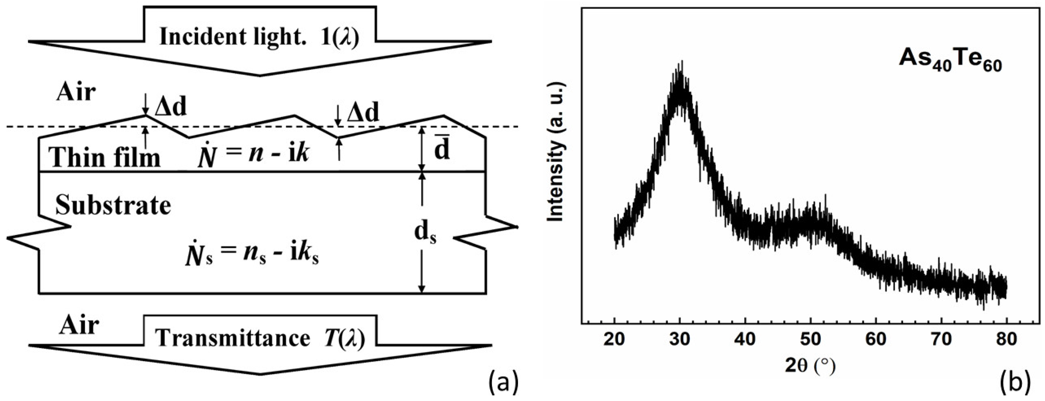
2. Materials and Methods

2.1. An Alternative Approach for Computing k (λ)

As already mentioned, k(λ) in the EMs has been computed by using equation for either Tsm(λ) or T+(λ), as both equations have been derived assuming the light passing through the film to be coherent. However, it was also commented that Tsm(λ) and especially T+(λ) can be influenced by partial coherence of the light due to light scattering from the film. In this regard, it was pointed out in [19,39] that the dependence:
T i ( λ ) = T + ( λ ) T ( λ )
represents the interference free transmittance of the specimen. Therefore, Ti(λ) does not depend on whether the light passing through the film is coherent or partially coherent. Moreover, an accurate formula for T(λ) is derived by replacing
φ = 4 π n [ d ¯ + ( d d ¯ ) ] / λ from Eq . ( 3 ) for T ( λ ) = 2 π . ( half integer ) + 4 π n ( d d ¯ ) / λ in Equation (1), as:
T ( λ ) = 1 φ 2 φ 1 φ 1 φ 2 T u ( φ ) d φ = ( τ a , f τ f , s τ s , a ) 2 x s φ 2 φ 1 φ 1 φ 2 x d φ a 1 b 1 cos ( φ ) + c 1 sin ( φ ) ,
where φ = 4 π n ( d d ¯ ) / λ + π , φ 1 = 4 π n Δ d / λ + π , φ 2 = 4 π n Δ d / λ + π . Furthermore, the accuracy of computation of Ti(λ) should be higher than that of T+(λ) and T(λ), whose errors are usually with opposite signs due to partial coherence of the light passing through the film and Ti(λ) is significantly smoother than Tsm(λ).
Taking into account the above comments from this Section, replacing the known values of T+(λ), T(λ), d ¯ , ∆d, and n(λ) in Equation (8), followed by its solution, can provide the unknown k[Ti(λ)] of the film for every λ. In film characterization based on the AOEM, since different k(λ) are computed e.g., from Tsm(λ) and Equations (1) and (5), T+(λ) and Equation (2), and Ti(λ) and Equation (8), the extinction coefficient of the film is selected to be k(λ) corresponding to the smallest FOM from Equation (7) [29].

2.2. Dual Transformation Regarding Tsm (λ) Taking into Account the Substrate Absorption

Although UV/VIS/NIR spectrophotometers provide light with λ ≈ 3000 nm [40,41], characterization of a film on glass substrate has not been performed by EM for λ > 2500 nm, as far as we know, since T(λ > 2500 nm) is significantly distorted due to large absorption in the glass. In order to characterize a film on a glass substrate including the region λ > 2500 nm, in this study is proposed and employed a dual transformation of transmittance spectra, consisting of a forward transformation and a reverse transformation.
In regard to the above, Tsm(λ) from Equation (1), T+(λ) from Equation (2), T(λ) from Equation (9), and Ti(λ) from Equation (8) are proportional to the first degree of the substrate absorbance 0 < xs(λ) ≤ 1, as both xs(λ) and Ts(λ) of glass substrate can be significantly smaller at λ > 2500 nm. Accordingly, the proposed forward transformation includes calculation of T(λ)’ = T(λ)/xs(λ) and its smoothing providing Tsm(λ)’, which represents an approximation of the transmittance of the specimen whose substrate is replaced by a transparent one. Next, the envelopes T+(λ)’ and T(λ)’ of Tsm(λ), and Ti(λ)’ = [T+(λ)’T(λ)’]0.5 are computed based on the algorithm from [30], and all their tangency wavelengths λt(i) with Tsm(λ)’ are determined, completing the forward transformation of transmittance spectra. Thereafter, the first stage of the AOEM is executed by using the points T+(λt)’ and T(λt)’. However, excluding the several longest λt for which xs(λt) << 1 since xs(λ) is present not only in the numerator of Equations (2) and (9), and substituting the film absorbance by xs(λt)’ = xs(λt)/xs(λt) = 1. At the end of such first stage of the AOEM, d ¯ , ∆d ≥ 0 and m1 are computed as in [28,29].
In the reverse transformation, Tsm(λ) = Tsm(λ)’xs(λ) are calculated, its envelopes T+(λ) = T+(λ)’xs(λ) and T(λ) = T(λ)’xs(λ), and Ti(λ) = Ti(λ)’xs(λ). Importantly, the tangency wavelengths of Tsm(λ) are the same as the already determined λt(i) since Tsm, T+ and T are represented by multiplying their respective Tsm’, T+’ ≥ Tsm’ and T’ ≤ Tsm’ by the same xs > 0, for every λ. After Tsm(λ), T+(λ), T(λ), Ti(λ) and all λt(i) are computed, the second stage of the AOEM can be executed as in [29] taking into account the substrate absorbance xs(λ) ≤ 1.

2.3. Calculation of a Lower Limit of n(λ)

An expression about the refractive index of a uniform film on a non-transparent substrate was presented in [35]:
n ( λ ) = M 1 + M 1 2 n s 2 , where M 1 ( λ ) = 2 n s T u + T u T u + T u + n s 2 + 1 2 ,
as Tu+(λ) and Tu−(λ) are the upper and lower envelopes of the smoothed transmittance spectrum of the respective specimen with uniform film.
Furthermore, the following relations are valid for a specimen with the same characteristics except that the film, with the same d ¯ , is non-uniform:
T + ( λ ) T u + ( λ ) , T ( λ ) T u ( λ )
where T+(λ) and T(λ) are the upper and lower envelopes of the smoothed transmittance spectrum Tsm(λ) of this specimen with non-uniform film [29,39]. Moreover, let us consider the quantity:
n l ( λ ) = M 2 + M 2 2 n s 2 , where M 2 ( λ ) = 8 n s 2 T + T T + T ( n s + 1 ) 2 x s ( n s 1 ) 2 x s + n s 2 + 1 2 .
It is deduced from Equations (10)–(12) that:
n ( λ ) n l ( λ ) ,  
showing that nl(λ) represents a lower limit of n(λ).

3. Results

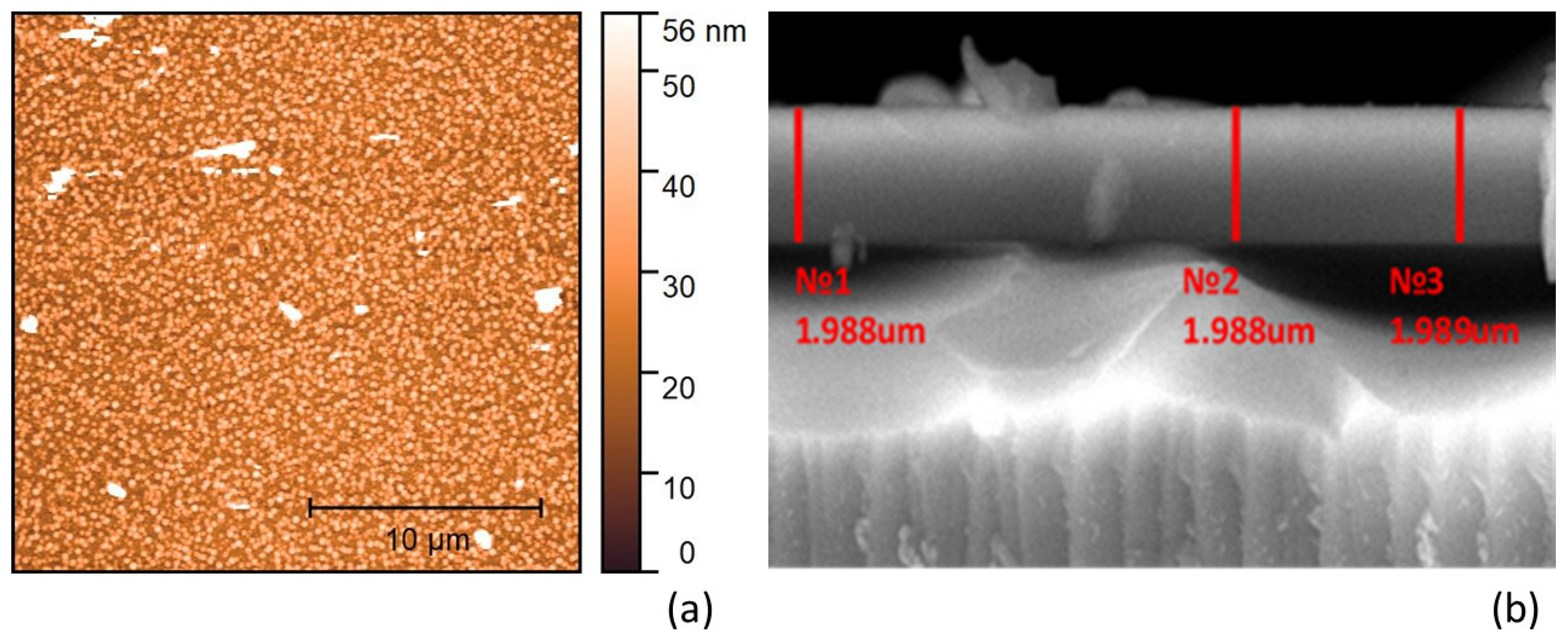
3.1. Measurements Regarding the Studied AsxTe100–X Films

The chemical composition and thickness of the films have been measured by energy-dispersive X-ray microanalysis (EDS) and scanning electron microscope (SEM) using JSM IT-300LV SEM of JEOL with an energy-dispersive attachment X-MaxN 20 of Oxford Instruments at high vacuum and an accelerating voltage of 20 kV. The compositions of the three studied films have been determined as As40Te60, As80Te20, and As98Te2 in [38].
X-ray diffraction (XRD) of film on glass substrate specimens are performed on a Shimadzu XRD-7000 X-ray diffractometer at a fixed time in the range of 10–80° with a step of 0.02°, using CuKα radiation with a wavelength of 1.5406 nm and scanning speed of 2° per minute. The XRD image for the As40Te60 film on a glass substrate from Figure 1b shows amorphous structure of the film, since the image does not contain any sharp peaks inherent to crystallites. Besides, there are two halos in the XRD image from Figure 1b, the stronger in the range of 2θ = 20–40°, and the weaker at 40–60°. The presence of these features presumably indicates presence of tellurium in the form of chains, and a small amount of AsTe3/2 trigonal pyramidal structural units, as confirmed by Raman spectroscopy data in [38]. Furthermore, the As80Te20 and As98Te2 films also have amorphous structures revealed by similar XRD images.
The surface morphology of the films was monitored at atmospheric conditions using Smena atomic force microscopy (AFM) head, based on the NTEGRA Spectra using HA_NC and HA_C probes NT-MDT (Zelenograd, Russia), in contact and semi-contact mode. Two-dimensional image of the surface and cross-section of the As98Te2 film are shown in Figure 2. The surface root-mean-square roughness Rq is determined from AFM image by Gwyddion open software [38]. Rq is 7.7 ± 0.7 nm for the As40Te60 film [38], 6.6 ± 0.7 nm for the As80Te20 film [38], and 8.1 ± 0.7 nm for the As98Te2 film from Figure 2a. Unfortunately, the As40Te60 and As80Te20 films have been destroyed without independent measurement of their average film thickness d ¯ .
A sample containing the As40Te60 film has been prepared by five minutes deposition onto 0.45 mm thick sapphire plate with double-sided polishing manufactured by Monocrystal [38,42]. Samples including the As80Te20 film or the As98Te2 film have been formed by deposition onto 1 mm thick standard microscope slide glass substrate of Levenhuk [38,43]. Normal incidence transmittance spectra T(λ) and Ts(λ) of these three samples and their substrates, as well as reflectance spectra Rs(λ) of the substrates have been measured by a Cary 5000 double-beam spectrophotometer of Agilent [44]. These transmittance spectra measurements have been implemented at room temperature, with a step of 1 nm, slit width of 3.44 nm, and a circular light spot with 1 mm diameter [38].
The substrate characteristics ns(λ) and ks(λ) are computed by solving the system of two equations about Ts(λ) and Rs(λ), for every λ, as in [27]. Every smoothed spectrum Tsm(λ) of a studied sample is computed by “external smoothing” of its T(λ), as described in the fifth paragraph of the Introduction and in [29]. Data and results regarding the characterization of the three AsxTe100–x films based on the AOEM are presented in the next three figures, whereas the results referring to λt(i) are exhibited by open circles, and the most important computed results are in red color. The optimized curve fittings for deriving n(λ) and k0(λ) are performed as described in Equation (6).

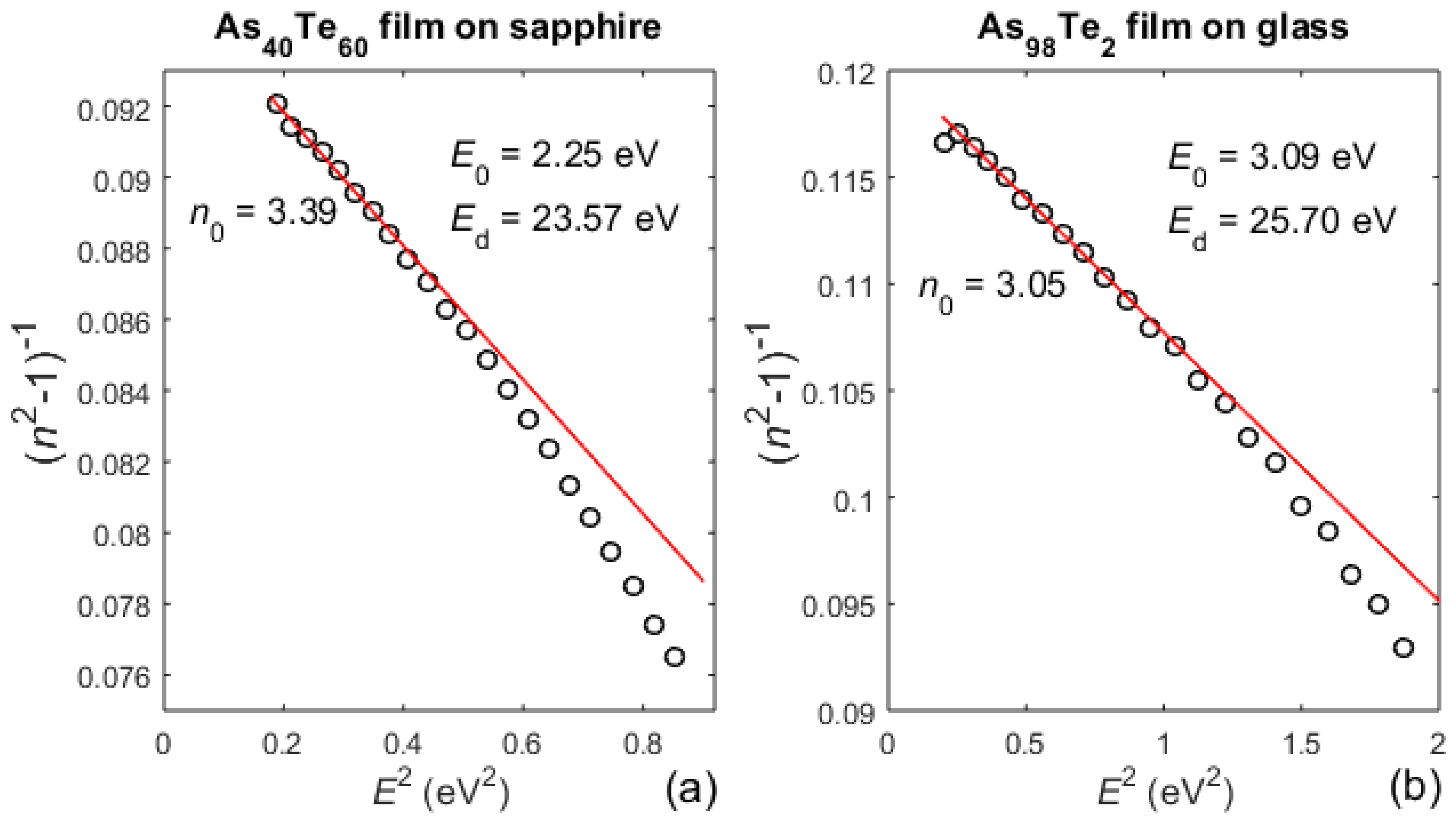
3.2. Characterization of the As40Te60 Film on Sapphire Substrate by the AOEM

Since sapphire is quasi-transparent over the used interval of λ [45], its xs(λ) ≅ 1, Ts(λ)~xs(λ) ≅ constant [27], and the AOEM is executed as in [29], except for absence of adjustment of the envelopes T+(λ) and T(λ) for substrate absorption. Data and characterization results for the As40Te60 film are shown in Figure 3. The values of d ¯ , ∆d ≥ 0 and m1 computed at the end of the first stage of the AOEM are typed in Figure 3b.
It is seen from Figure 3b that the refractive index n(λ) of the film decreases with increasing λ, i.e., it has a normal dispersion in the whole studied spectral range, and n(λ) is larger than its lower limit nl(λ) in accordance with Equation (13). Furthermore, Figure 3c,e show that the film has a wide spectral region of quasi-transparency, i.e., a region with negligibly small k(λ).

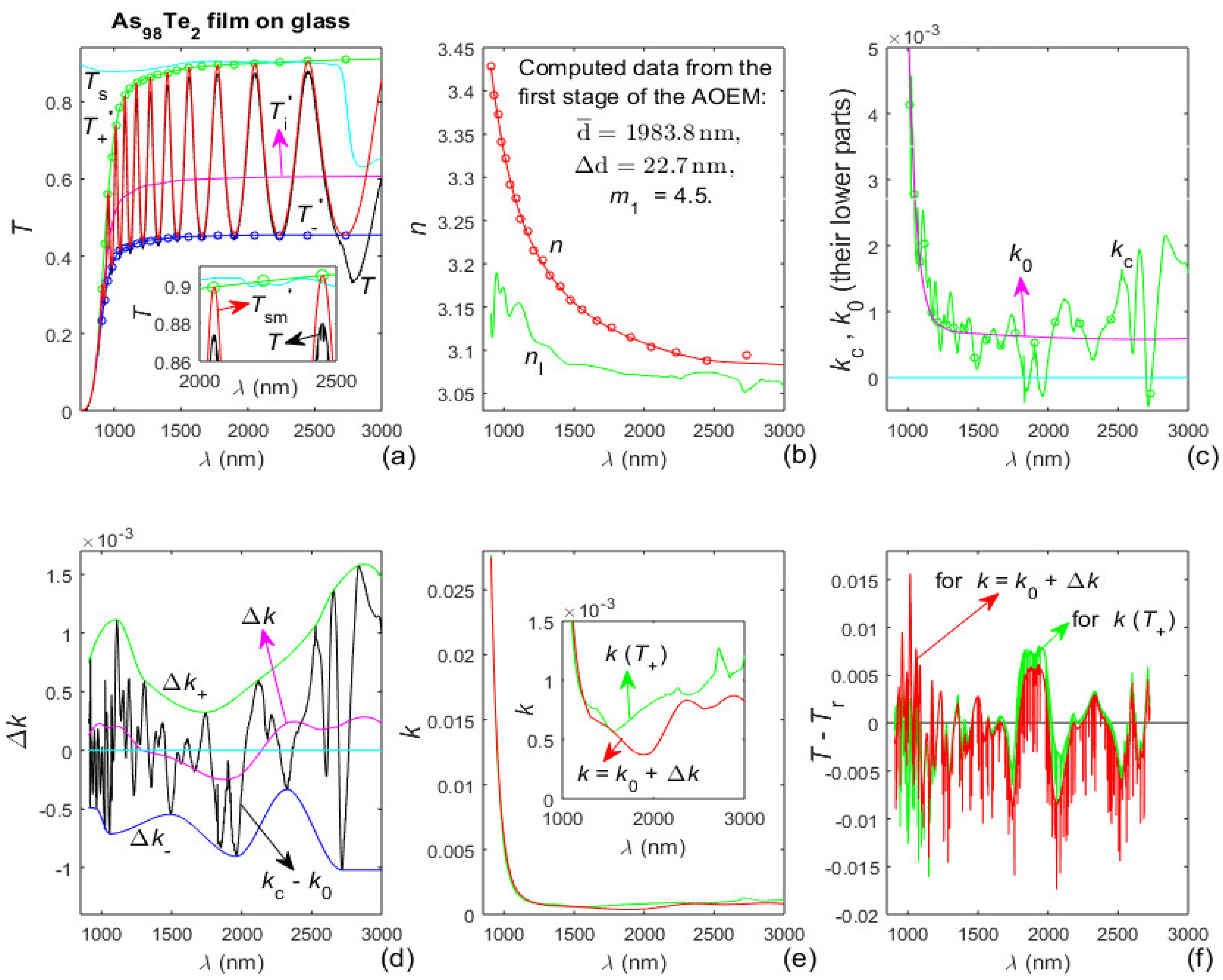
3.3. Characterization of the As98Te2 Film on Glass Substrate by the AOEM

The As98Te2 film has been deposited for fifteen minutes on a glass substrate described in Section 3.1 [38]. Such glass substrates are strongly absorbing for λ > 2500 nm as revealed by the significantly lower values of Ts(λ > 2500 nm) from Figure 3a. Therefore, the dual transformation regarding Tsm(λ), described in Section 2.2 is employed, as the first stage of the AOEM is implemented excluding only the longest λt(i) since only it is within the region of significantly lower values of Ts(λ). Data and results from the characterization of the As98Te2 film by the AOEM are exhibited in Figure 4.
It is seen from Figure 4a that Tsm(λ)’, T+(λ)’ and T(λ)’, obtained by the forward transformation described in Section 2.2, do not change their appearance in the region λ > 2500 nm of strong absorption in the substrate, unlike the significantly lower Ts(λ) and T(λ) there. This allows accurate computation of Tsm(λ)’, T+(λ)’, T(λ)’, Ti(λ)’ and λt(i); followed by accurate computation of Tsm(λ), T+(λ), T(λ) and Ti(λ) by the reverse transformation described in Section 2.2. Figure 4b shows that n(λ) has a normal dispersion in the whole studied spectral range and n(λ) > nl(λ). Besides, the film also has a wide spectral region of quasi-transparency-Figure 4c,e. Notably, the difference between the average film thickness d ¯ = 1983.8 nm from Figure 4b computed by the AOEM and d ¯ = 1988.3 nm from the SEM image from Figure 2b is 0.24%.
The positive partially coherent light correction Δk(λ) ≈ 2 × 10⁻⁴ for the As40Te60 film, seen from Figure 3d, is attributed to light scattering from this relatively thick film resulting in slight shrinkage of the interference pattern of T(λ) [29]. The positive or negative Δk(λ) for the As98Te2 film from Figure 4d is ascribed to smaller light scattering from this thinner film being sufficiently counterbalanced by the external smoothing of T(λ).

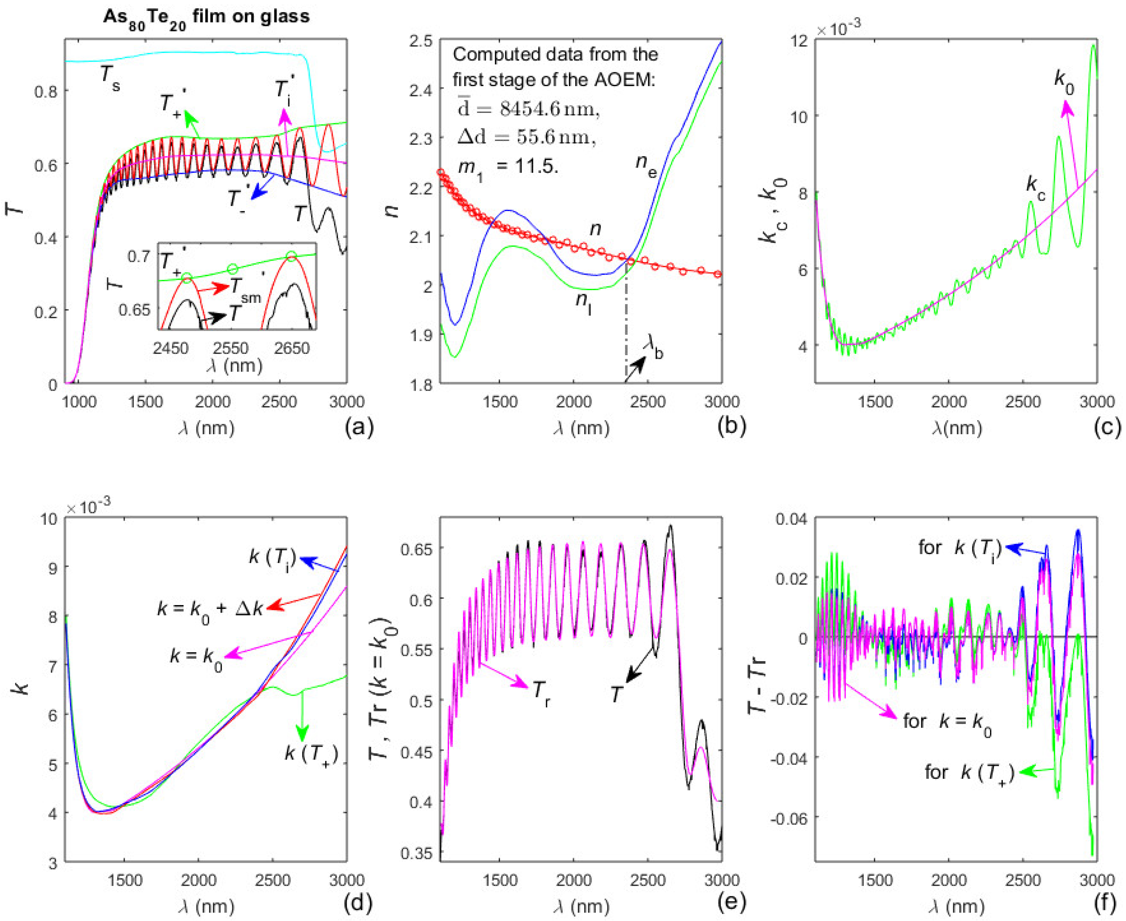
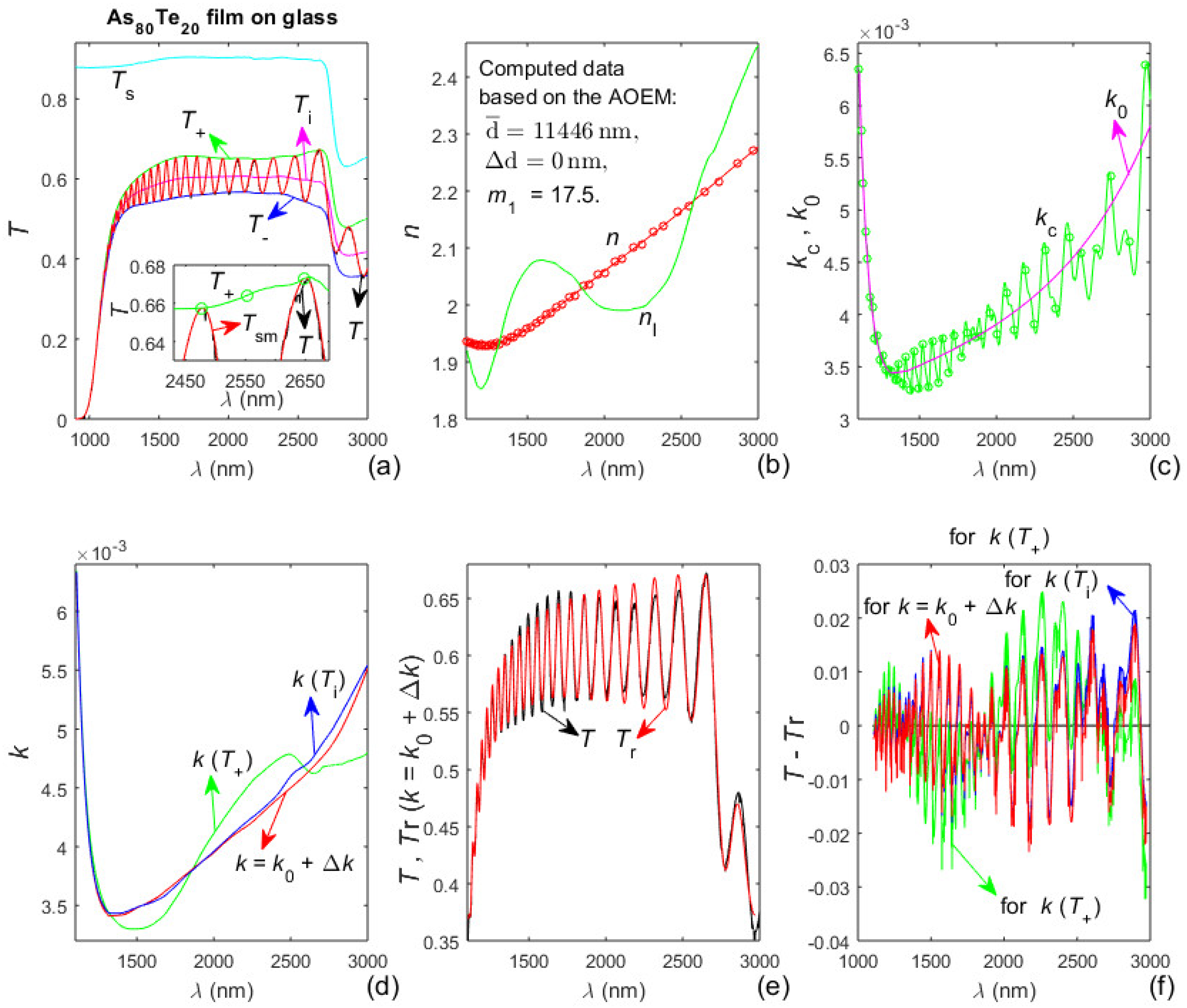
3.4. Characterization of the As80Te20 Film on Glass Substrate Based on the AOEM

The As80Te20 film has been deposited for thirty minutes on a glass substrate described in Section 3.1 [38]. The dual transformation regarding Tsm(λ) is implemented, as the first stage of the AOEM is executed excluding the four longest λt(i) since they are within the region of significantly lower values of Ts(λ) from Figure 5a. Data and results from the characterization of the As80Te20 film by the AOEM are presented in Figure 5, as the optimized number of λt(i) participating in the first stage of the characterization is n = 26. The dependence ne(λ) from Figure 5b is determined by substituting the already computed T+(λ), T(λ), d ¯ , ∆d, and m1 in Equations (2) and (9) of the envelopes. Solving these two equations with respect to the two unknown ne and ke components of the complex refractive index of the film, for every λ. The longest wavelength of n(λ) crossing ne(λ) is denoted by λb in Figure 5b.
A comparison of T(λ) from Figure 3a, Figure 4a and Figure 5a shows that the As80Te20 film has quite different optical characteristics with respect to the As40Te60 and As98Te2 films. For example, the much narrower interference pattern of T(λ) from Figure 5a demonstrates that the refractive index n(λ) of the As80Te20 film is significantly smaller than that of the As40Te60 and As98Te2 films, as explained in [19]. Also, the more than twice larger number Ne of extrema of Tsm(λ) from Figure 5a indicates that the product n(λ) d ¯ for the As80Te20 film is at least twice larger than that for the As40Te60 and As98Te2 films, as implied by Equation (3). The above data show that the average thickness of the As80Te20 film is significantly larger than 2 d ¯ = 6613.8 nm of the As40Te60 film.
Also, the difference Ts(λ) − T+(λ) is much larger in the region of the interference pattern from Figure 5a than for the As40Te60 and As98Te2 films, indicating significantly stronger absorption and larger k(λ) of the As80Te20 film. Moreover, Ti(λ) from Figure 5a decreases with increasing λ above 2300 nm implying increasing absorption there, which can be attributed to anomalous dispersion in this region. Besides, the difference T+(λ) − T(λ) from Figure 3a and Figure 4a does not have an apparent minimum in the region of the interference pattern. However, T+(λ) − T(λ) regarding Figure 5a rises with increasing λ above its apparent minimum at λ ≈ 2100 nm, indicating increasing n(λ) for λ > 2100 nm, thus confirming the presence of anomalous dispersion within the studied spectral region of the As80Te20 film.
Furthermore, it is seen from Figure 5b that the respective characterization of the As80Te20 film by the AOEM does not recognize the commented above presence of anomalous dispersion. It is also apparent from Figure 5b that the difference nl(max(λ)) − n(max(λ)) is too large, as n(λ > λb) < ne(λ > λb) ≈ nl(λ > λb) although nl(λ) should be a lower limit of n(λ) according to Equation (13). Moreover, the difference |T(λ > 2600 nm) − Tr(λ > 2600 nm)| reaches too large values in Figure 5f compared to Figure 3f and Figure 4f. These facts show that the represented in Figure 5 characterization of the As80Te20 film by the AOEM is inaccurate in the region of anomalous dispersion of the film. A main reason for this is the exclusion of the four longest λt(i) from the execution of the first stage of the AOEM characterization corresponding to Figure 5, taking into account that these λt(i) also belong to the region of anomalous dispersion where T+(λ) − T(λ) rises significantly with increasing λ.
Importantly, accurate film characterization by any EM requires determination of the correct first interference order m1, which has integer or half-integer value, since it imposes a narrow interval of possible values of the average film thickness d ¯ in accordance with Equation (3). Correspondingly, the failure of the characterization of the As80Te20 film by the AOEM represented by Figure 5 to recognize the presence of anomalous dispersion is attributed to determination of incorrect m1.
Aiming at selection of the correct m1, a simplified AOEM is employed by fixing both m1 to every possible value from Equation (3) and the number of used extrema of Tsm(λ) to Ne, for each one of the three films. At the second stage of the respective simplified characterizations of the film, k(Ti) computed from Equation (8) is used as described in Section 2.1. The main results from these computations are given in Table 1.
It is seen from Table 1 that the smallest δd/n and FOM correspond to the same m1 for each one of the As40Te60 and As98Te2 films, thus confirming the accuracy of their characterizations represented by Figure 3 and Figure 4. Furthermore, this justifies the main concept of the OEM and the AOEM that computation of d ¯ , ∆d, and m1 corresponding to the smallest δd/n is required for accurate computation of n(λ) and k(λ) of the characterized thin dielectric or semiconductor film with d ¯ = (300,5000) nm.
However, the smallest δd/N and the smallest FOM correspond to different values of m1 for the significantly thicker As80Te20 film. Since the film characterization should provide reconstructed transmittance spectrum Tr(λ) as close as possible to T(λ), another characterization of the As80Te20 film is performed based on using the AOEM with the values of d ¯ , ∆d, and m1 listed in red in Table 1. Data and results from this characterization are shown in Figure 6.
Notably, it is seen from Figure 6b that its corresponding characterization recognizes the presence of anomalous dispersion for the As80Te20 film, as the difference nl(max(λ)) − n(max(λ)) is significantly smaller than for the characterization from Figure 5. This warrants the procedure for AOEM characterization of films thicker than 5000 nm, by selection of m1 based on determination of min{FOM (m1,k(Ti))}, exemplified by the use of Table 1 for the As80Te20 film.

3.5. Additional Results about the AsxTe100−X Films

Other data regarding characterizations of the three studied films based on the AOEM are presented in Table 2, as the data about the As40Te60 and As98Te2 films refer to the characterizations represented by Figure 3 and Figure 4. The data related to the As80Te20 film and designated as “m1 = 11.5, ND” and “m1 = 17.5, AD” refer to the characterizations represented by Figure 5 and Figure 6 respectively, as “ND” denotes normal dispersion and “AD”—anomalous dispersion. Since n(λ) from Figure 5b does not demonstrate anomalous dispersion and its respective nl(max(λ)) − n(max(λ)) is quite large, one more characterization of the As80Te20 film is performed using the film data typed in Figure 5b and n(λλb) from Figure 5b, however employing n(λ > λb) = ne(λ > λb). Taking into account that this characterization recognizes the presence of anomalous dispersion, it is denoted as “m1 = 11.5, AD”. However, the FOM data from Table 2 show that this particular characterization is most inaccurate amongst the three represented there characterizations of the As80Te20 film.
Importantly, a comparison of the data from the fourth and fifth columns of Table 2 shows that the extinction coefficient of the film is computed more accurately from Ti(λ) and Equation (8) rather than from T+(λ) and Equation (2), for all five film characterizations based on the AOEM. This is mainly attributed to the independence of Ti(λ) from possible partial coherence of the light passing through the film and light scattering from the film, as discussed in Section 2.1.
The Wemple–DiDomenico (WD) single-effective-oscillator approximation n ( E ) 1 + E 0 E d E 0 2 E 2 is known to be valid for amorphous semiconductors and glasses, where E0 is the oscillator energy, Ed is the dispersion energy, and E(eV) = 1.2398/λ (µm) is the photon energy [46]. Regardingly, in Figure 7 are presented WD plots {n(E(λt))2−1}−1 versus E(λt)2 [46] for the As40Te60 and As98Te2 films. The parameters E0 and Ed are determined by a low-energy linear regression to the WD plot, and the static refractive index is n 0 = n ( E = 0 )     1 + E d / E 0 .
The dispersion energy, Ed, measures the average strength of the interband optical transitions, and has been found to obey the empirical relationship [46]:
E d ( eV ) = β N c Z a N v
where β = βc = 0.37 ± 0.04 eV in ‘covalent’ materials, β = βio = 0.26 ± 0.03 eV in ‘ionic’ materials, Nc is the coordination number of the cation nearest neighbor to the anion, Za is the formal chemical valence of the anion, and Nv is the total number of valence electrons (cores excluded) per anion. Using Ed typed in Figure 7, Equation (14), and β = βc is estimated the coordination number of the cation (As) to be Nc ≈ 3.5 for the As40Te60 film, and Nc ≈ 3.56 for the As98Te2 film.
Furthermore, E0 for the As80Te20 film is significantly smaller than for the As40Te60 and As98Te2 films, taking into account that its n(E) is also significantly smaller in accordance with Figure 3b, Figure 4b, and Figure 6b and the WD approximation. Since min(E) is too close to E0 for the As80Te20 film, anomalous dispersion occurs and low-energy linear regression to the WD plot cannot be used for accurate determination of E0, Ed, and n0.

4. Discussion

The OEM [28] was developed for increasing the accuracy of characterization of a thin film on a substrate from interference T(λ) of the specimen, by optimization of the three parameters of the IEM from [27], accounting for possible non-uniformity of the film and substrate absorption. It was demonstrated in [34] that the OEM from [28] provides most accurate characterization of a-Si films with dissimilar thicknesses compared to the OGM [35], TLUM [36], and CLUM [37] selected as the most likely methods for accurate characterization of these films. Further increasing the characterization accuracy was achieved by the AOEM [29] based on: external smoothing of T(λ) offsetting the influence of light scattering, enhanced computation of the envelopes using both iteration and extra points, and computation of n(λ) and k(λ) by optimized curve fitting.
In the first stage of the AOEM, the average thickness d ¯ , the thickness non-uniformity ∆d over the light spot, and the first interference order m1 of the film are computed, by minimization of the error metric, usually δd/N > 0. This error metric can be used for estimation of the relative error δd/ d ¯ = δd/N. (N/ d ¯ ) in the computation of d ¯ of the characterized film. In order to compare the accuracy of computation of d ¯ , in Table 3 are presented data about the relative error δd/ d ¯ for the presented here characterizations of AsxTe100−x films and for recent characterizations of a-Si and As33S67 based on the FEM and the AOEM.
Notably, the films characterized based on the FEM have been developed to be uniform, deposited on quasi-transparent substrates, and d ¯ of the films from [47] has been chosen to provide neither too high nor too low values of m1, as all of these factors are favorable for accurate film characterization. Nevertheless, it is seen from Table 3 that the characterization of films based on the AOEM provides significantly smaller relative error δd/ d ¯ , and therefore more accurate d ¯ , in comparison with the characterizations based on the FEM; the only exception being the As80Te20 film.
The record low value of δd/ d ¯ = 0.101% in Table 3 is for the As40Te60 film and it is associated with the quasi-transparency of its sapphire substrate, unlike the absorption of the glass substrates. The fact that the second lowest δd/ d ¯ = 0.133% from Table 3 is for the As98Te2 film is believed to be mostly due to a superior accuracy of its respective envelopes T+(λ) and T(λ) as a result of the implementation of the proposed here dual transformation regarding Tsm(λ).
Furthermore, the relative error in the computation of the refractive index of the film is δn/n = δd/ d ¯ + δλt/λt, according to Equation (3), where δλt/λt is the relative error in computation of λt. Justifiably assuming δλt/λt ≤ 0.15% [28,29,30] leads to δn/n < 0.3% for the characterizations of the As40Te60 and As98Te2 films by the AOEM represented by Figure 3 and Figure 4. The significantly smaller n(λ) and larger k(λ) of the As80Te20 film are attributed to some porosity, oxidation in the film, and its non-stoichiometry in comparison with the As40Te60 and As98Te2 films. In this regard, anomalous dispersion has already been observed for other chalcogenide thin films [49].

5. Conclusions

The AOEM is employed for optical characterization of three AsxTe100−x films with different compositions and dissimilar d ¯ , only from a normal incidence interference transmittance spectrum T(λ ≤ 3000 nm) of a specimen consisting of the film on a substrate. To cope with the strong light absorption in commonly used glass substrates for λ > 2500 nm, a dual transformation of T(λ) is proposed and implemented for accurate computation of its envelopes T+(λ) and T(λ). This dual transformation is simpler and should provide more accurate envelopes of T(λ) in comparison with the computation of the envelopes from [29], in case of non-transparency of the substrate. The accuracy of computation of d ¯ is record low <0.15%, implying <0.3% accuracy of computation of n(λ) of the As40Te60 and As98Te2 films by the AOEM.
It is justified that the As80Te20 film exhibits a region of anomalous dispersion and is significantly thicker than 6600 nm, which makes it very difficult for characterization by envelope method. In this respect, a procedure is proposed for accurate determination of the first interference order m1 for such a thick film, and this procedure is used for characterization of the As80Te20 film based on the AOEM. As far as we are aware of, the As80Te20 film is the only one with anomalous dispersion and the thickest, with estimated d ¯ = 11446 nm, ever characterized by an envelope method.
It is also pointed out that Ti(λ) does not depend on the scattering of light from the film, unlike T+(λ). Consequently, it is shown that computation of k(λ) from Ti(λ) and Equation (8) is more accurate than the commonly employed computation of k(λ) from T+(λ) and Equation (2), for all five characterizations of AsxTe100−x films based on the AOEM and represented in Table 2.
The obtained results strengthen our conviction that the AOEM has a capacity for providing most accurate optical characterization of almost every dielectric or semiconductor film with d ¯ > 300 nm on a substrate compared to all the other methods for characterization of such films only from T(λ).

Author Contributions

Conceptualization, D.M., G.A., R.N., and A.N.; methodology, D.M., G.A., R.N., and A.N.; software, D.M. and R.N.; validation, D.M., R.N., and A.N.; formal analysis, D.M. and R.N.; investigation, D.M., R.N., and A.N.; resources, D.M., R.N., and A.N.; data curation, D.M., R.N., A.N., M.K., and A.M.; writing—original draft preparation, D.M. and R.N.; writing—review and editing, G.A., D.U., and A.N.; visualization, D.M., R.N., and A.N.; supervision, D.M., G.A., and D.U.; project administration, G.A., M.K., and A.M.; funding acquisition, G.A. and D.U. All authors have read and agreed to the published version of the manuscript.

Funding

This work was supported by the European Regional Development Fund within the Operational Programme “Science and Education for Smart Growth 2014–2020” under the Project CoE “National Center of Mechatronics and Clean Technologies”, Contract No. BG05M2OP001-1.001-0008, L10S7 SynChaLab. The AsxTe100−x film on substrate specimens have been prepared with funding from the Russian Science Foundation grant 16-12-00038.

Conflicts of Interest

The authors declare no conflict of interest.

References

  1. Soriaga, M.P.; Stickney, J.; Bottomley, L.A.; Kim, Y.G. Thin Films: Preparation, Characterization, Applications, 1st ed.; Springer: Boston, MA, USA, 2002; pp. 37–45. [Google Scholar]
  2. Aliofkhazraei, M. Anti-Abrasive Nanocoatings Current and Future Applications, 1st ed.; Woodhead Publishing: Cambridge, UK, 2015; pp. 543–567. [Google Scholar]
  3. Frey, H.; Khan, H.R. Handbook of Thin Film Technology, 1st ed.; Springer: Berlin, Germany, 2015; pp. 24–41. [Google Scholar]
  4. SeshanIntel, K. Handbook of Thin-Film Deposition Processes and Techniques, 2nd ed.; William Andrew Publishing: New York, NY, USA, 2002; pp. 64–76. [Google Scholar]
  5. Stenzel, O. Optical Coatings: Material Aspects in Theory and Practice, 1st ed.; Springer: Heidelberg, Germany, 2016; pp. 35–51. [Google Scholar]
  6. Poelman, D.; Smet, P.J. Methods for the determination of the optical constants of thin films from single transmission measurements: A critical review. J. Phys. D 2003, 36, 1850–1857. [Google Scholar] [CrossRef]
  7. Stenzel, O. The Physics of Thin Film Optical Spectra, 1st ed.; Springer: Heidelberg, Germany, 2016; pp. 79–81. [Google Scholar]
  8. Minkov, D.A. DSc Thesis: Characterization of Thin Films and Surface Cracks by Electromagnetic Methods and Technologies; Technical University: Sofia, Bulgaria, 2018; pp. 114–119. [Google Scholar]
  9. Tauc-Lorentz_Dispersion_Formula.pdf, Technical Note. Spectroscopic Ellipsometry TN11. Available online: https://www.horiba.com/fileadmin/uploads/Scientific/Downloads/OpticalSchool_CN/TN/ellipsometer/Tauc-Lorentz_Dispersion_Formula.pdf (accessed on 6 June 2020).
  10. Gao, L.; Lemarchand, F.; Lequime, M. Comparison of different dispersion models for single layer optical thin film index determination. Thin Solid Films 2011, 520, 501–509. [Google Scholar] [CrossRef]
  11. Mieghem, P.V. Theory of band tails in heavily doped semiconductors. Rev. Mod. Phys. 1992, 64, 755–793. [Google Scholar] [CrossRef]
  12. Fedyanin, D.Y.; Arsenin, A.V. Surface plasmon polariton amplification in metal-semiconductor structures. Opt. Express 2011, 19, 12524–12531. [Google Scholar] [CrossRef]
  13. Cisowski, J.; Jarzabek, B.; Jurusik, J.; Domanski, M. Direct determination of the refraction index normal dispersion for thin films of 3, 4, 9, 10-perylene tetracarboxylic dianhydride (PTCDA). Opt. Appl. 2012, 42, 181–192. [Google Scholar]
  14. Grassi, A.P.; Tremmel, A.J.; Koch, A.W.; El-Khozondar, H.J. On-line thickness measurement for two-layer systems on polymer electronic devices. Sensors 2013, 13, 15747–15757. [Google Scholar] [CrossRef] [Green Version]
  15. Brinza, M.; Emelianova, E.V.; Adriaenssens, G.Y. Nonexponential distributions of tail states in hydrogenated amorphous silicon. Phys. Rev. B 2005, 71, 115209. [Google Scholar] [CrossRef]
  16. Swanepoel, R. Determining refractive index and thickness of thin films from wavelength measurements only. J. Opt. Soc. Am. A 1985, 2, 1339–1343. [Google Scholar] [CrossRef]
  17. Minkov, D.A. Computation of the optical constants of a thin dielectric layer on a transmitting substrate from the reflection spectrum at inclined incidence of light. J. Opt. Soc. Am. A 1991, 8, 306–310. [Google Scholar] [CrossRef]
  18. Minkov, D.A. Calculation of the optical constants of a thin layer upon a transparent substrate from the reflection spectrum. J. Phys. D 1989, 22, 1157–1161. [Google Scholar] [CrossRef]
  19. Swanepoel, R. Determination of the thickness and optical constants of amorphous silicon. J. Phys. E 1983, 16, 1214–1222. [Google Scholar] [CrossRef]
  20. Swanepoel, R. Determination of the Thickness and Optical Constants of Amorphous Silicon. Google Scholar. Available online: https://scholar.google.com/scholar?hl=bg&as_sdt=0%2C5&q=R.+Swanepoel+1983&btnG= (accessed on 6 June 2020).
  21. Chiao, S.C.; Bovard, B.G.; Macleod, H.A. Optical-constant calculation over an extended spectral region: Application to titanium dioxide film. Appl. Opt. 1995, 34, 7355–7359. [Google Scholar] [CrossRef] [PubMed]
  22. Gonzalez, J.S.; Parralejo, A.D.; Ortiz, A.L.; Guiberteau, F. Determination of optical properties in nanostructured thin films using the Swanepoel method. Appl. Surf. Sci. 2006, 252, 6013–6017. [Google Scholar] [CrossRef]
  23. Gao, L.; Lemarchand, F.; Lequime, M. Refractive index determination of SiO2 layer in the UV/Vis/NIR range: Spectrophotometric reverse engineering on single and bi-layer designs. J. Europ. Opt. Soc. Rap. Public. 2013, 8, 13010. [Google Scholar] [CrossRef] [Green Version]
  24. Yen, S.T.; Chung, P.K. Extraction of optical constants from maxima of fringing reflectance spectra. Appl. Opt. 2015, 54, 663–668. [Google Scholar] [CrossRef]
  25. Jin, Y.; Song, B.; Jia, Z.; Zhang, Y.; Lin, C.; Wang, X.; Dai, S. Improvement of Swanepoel method for deriving the thickness and the optical properties of chalcogenide thin films. Opt. Express 2017, 25, 440–451. [Google Scholar] [CrossRef] [PubMed]
  26. Jin, Y.; Song, B.; Lin, C.; Zhang, P.; Dai, S.; Xu, T. Extension of the Swanepoel method for obtaining the refractive index of chalcogenide thin films accurately at an arbitrary wavenumber. Opt. Express 2017, 25, 31273–31280. [Google Scholar] [CrossRef] [PubMed]
  27. Leal, J.M.G.; Alcon, R.P.; Angel, J.A.; Minkov, D.A.; Marquez, E. Influence of substrate absorption on the optical and geometrical characterization of thin dielectric films. Appl. Opt. 2002, 41, 7300–7308. [Google Scholar] [CrossRef]
  28. Minkov, D.A.; Gavrilov, G.M.; Angelov, G.V.; Moreno, G.M.D.; Vazquez, C.G.; Ruano, S.M.F.; Marquez, E. Optimisation of the envelope method for characterisation of optical thin film on substrate specimens from their normal incidence transmittance spectrum. Thin Solid Films 2018, 645, 370–378. [Google Scholar] [CrossRef]
  29. Minkov, D.A.; Angelov, G.V.; Nestorov, R.N.; Marquez, E. Perfecting the dispersion model free characterization of a thin film on a substrate specimen from its normal incidence interference transmittance spectrum. Thin Solid Films 2020, 706, 137984. [Google Scholar] [CrossRef]
  30. Gavrilov, G.M.; Minkov, D.A.; Marquez, E.; Ruano, S.M.F. Advanced computer drawing envelopes of transmittance spectra of thin film specimens. Int. J. Adv. Res. Sci. Eng. Technol. 2016, 3, 163–168. [Google Scholar]
  31. McClain, M.; Feldman, A.; Kahaner, D.; Ying, X. An algorithm and computer program for the calculation of envelope curves. Comput. Phys. 1991, 5, 45–48. [Google Scholar] [CrossRef]
  32. Nestorov, R.N. Selection of error metric for accurate characterization of a thin dielectric or semiconductor film on glass substrate by the optimizing envelope method. Int. J. Adv. Res. Sci. Eng. Technol. 2020, 7, 1–11. [Google Scholar]
  33. Minkov, D. Method for determining the optical constants of a thin film on a transparent substrate. J. Phys. D 1989, 22, 199–205. [Google Scholar] [CrossRef]
  34. Minkov, D.A.; Angelov, G.V.; Nestorov, R.N.; Marquez, E.; Blanco, E.; Ruiz-Perez, J.J. Comparative study of the accuracy of characterization of thin films a-Si on glass substrates from their interference normal incidence transmittance spectrum by the Tauc-Lorentz-Urbach, the Cody-Lorentz-Urbach, the optimized envelopes and the optimized graphical methods. Mater. Res. Express 2019, 6, 03640. [Google Scholar]
  35. Minkov, D.A.; Gavrilov, G.M.; Moreno, J.M.D.; Vazquez, C.G.; Marquez, E. Optimization of the graphical method of Swanepoel for characterization of thin film on substrate specimens from their transmittance spectrum. Meas. Sci. Technol. 2017, 28, 035202. [Google Scholar] [CrossRef]
  36. DeMarcos, L.V.R.; Larruquert, J.I. Analytic optical-constant model derived from Tauc-Lorentz and Urbach tail. Opt. Express 2016, 24, 28561–28572. [Google Scholar]
  37. Ferlauto, A.S.; Ferreira, G.M.; Pearce, J.M.; Wronski, C.R.; Collins, R.W.; Deng, X.; Ganguly, G. Analytical model for the optical functions of amorphous semiconductors from the near-infrared to ultraviolet: Applications in thin film photovoltaics. J. Appl. Phys. 2002, 92, 2424–2436. [Google Scholar] [CrossRef] [Green Version]
  38. Mochalov, L.; Dorosz, D.; Nezhdanov, A.; Kudryashov, M.; Zelentsov, S.; Usanov, D.; Logunov, A.; Mashin, A.; Gogova, D. Investigation of the composition-structure-property relationship of AsxTe100−x films prepared by plasma deposition. Spectrochim. Acta A: Mol. Biomol. Spectrosc. 2018, 191, 211–216. [Google Scholar] [CrossRef]
  39. Swanepoel, R. Determination of surface roughness and optical constants of inhomogeneous amorphous silicon films. J. Phys. E: Sci. Instrum. 1984, 17, 896–903. [Google Scholar] [CrossRef]
  40. Scientific Instruments News. Technical Magazine of Electron Microscope and Analytical Instruments. Introduction to Model UH4150AD UV-Vis-NIR Spectrophotometer. Available online: https://www.hitachi-hightech.com/global/sinews/technical_explanation/080302/ (accessed on 6 June 2020).
  41. UV-3600i Plus UV-VIS-NIR Spectrophotometer. Available online: https://www.shimadzu.com/an/molecular_spectro/uv/uv-3600plus/features.html (accessed on 6 June 2020).
  42. Nanocrystal. Quality and Reliability. Available online: http://www.monocrystal.com/catalog/sapphire/plate/ (accessed on 6 June 2020).
  43. Levenhuk. Zoom&Joy. Available online: https://www.levenhuk.com/catalogue/accessories/levenhuk-n18-ng-prepared-slides-set/#.XsbUvmgzaUk (accessed on 6 June 2020).
  44. UV-Vis & UV-Vis-NIR Systems. Available online: https://www.agilent.com/en/products/uv-vis-uv-vis-nir/uv-vis-uv-vis-nir-systems/cary-5000-uv-vis-nir (accessed on 6 June 2020).
  45. Crystal Techno. Available online: http://www.crystaltechno.com/Al2O3_en.htm (accessed on 6 June 2020).
  46. Wemple, S.H. Refractive-index behavior of amorphous semiconductors and glasses. Phys. Rev. B. 1973, 7, 3767–3777. [Google Scholar] [CrossRef]
  47. Márquez, E.; Saugar, E.; Díaz, J.M.; García-Vázquez, C.; Ruano, S.M.F.; Blanco, E.; Ruiz-Pérez, J.J.; Minkov, D.A. The influence of Ar pressure on the structure and optical properties of nonhydrogenated a-Si thin films grown by rf magnetron sputtering onto room temperature glass substrates. J. Non-Cryst. Solids 2019, 517, 32–43. [Google Scholar] [CrossRef]
  48. Marquez, E.; Díaz, J.M.; García-Vazquez, C.; Blanco, E.; Ruiz-Perez, J.J.; Minkov, D.A.; Angelov, G.V.; Gavrilov, G.M. Optical characterization of amine-solution-processed amorphous AsS2 chalcogenide thin films by the use of transmission spectroscopy. J. Alloys Compd. 2017, 721, 363–373. [Google Scholar] [CrossRef]
  49. Abdel-Aal, A. The optical parameters and photoconductivity of CdxIn1Se9-x chalcogenide thin films. Physica B 2007, 392, 180–187. [Google Scholar] [CrossRef]
Figure 1. (a) A sketch of a homogeneous thin film on a substrate specimen, and its main optical characteristics [29]. (b) X-ray diffraction (XRD) image for a plasma deposited As40Te60 film on a glass substrate.
Materials 13 02981 g001
Figure 2. Surface and cross-section images of the As98Te2 film: (a) AFM picture; (b) scanning electron microscope (SEM) photo.
Materials 13 02981 g002
Figure 3. Input data and computed results from the characterization of the As40Te60 film by the advanced optimizing envelope method (AOEM). (a) Ts(λ), T(λ), Tsm(λ), its envelopes T+(λ) and T(λ), the points T+(λt) and T(λt) represented by circles, and Ti(λ); (b) n(λ) determined by optimized curve fitting over n0(λt) visualized by circles, and its lower limit nl(λ); (c) kc(λ) obtained from Equation (1) and its optimized curve fitted k0(λ); (d) deriving the partially coherent light correction Δk(λ) > 0; (e) k(T+) computed from Equation (2) and k = k0 + Δk; (f) difference between T(λ) and Tr(λ) computed using k(T+) and k = k0 + Δk, respectively.
Materials 13 02981 g003
Figure 4. Input data and computed results from the characterization of the As98Te2 film by the AOEM. (a) Ts(λ), T(λ), Tsm(λ)’, its envelopes T+(λ)’ and T(λ)’, the points T+(λt)’ and T(λt)’ represented by circles, and Ti(λ)’; (b) n0(λt) shown by circles, n(λ), and its lower limit nl(λ); (c) kc(λ) and its optimized curve fitted k0(λ); (d) deriving the partially coherent light correction Δk(λ); (e) k(T+) computed from Equation (2) and k = k0 + Δk; and (f) difference between T(λ) and Tr(λ) computed using k(T+) and k = k0 + Δk, respectively.
Materials 13 02981 g004
Figure 5. Input data and computed results from the characterization of the As80Te20 film by the AOEM. (a) Ts(λ), T(λ), Tsm(λ)’, its envelopes T+(λ)’ and T(λ)’, and Ti(λ)’; (b) n0(λt), n(λ), nl(λ) and ne(λ); (c) kc(λ) and its optimized curve fitted k0(λ); (d) k(T+) computed from Equation (2), k(Ti) from Equation (8) and k = k0 + Δk; (e) T(λ) and the reconstructed spectrum Tr(λ) computed using k = k0; and (f) difference between T(λ) and Tr(λ) with k = k0, k(T+) and k(Ti).
Materials 13 02981 g005
Figure 6. Input data and computed results from the characterization of the As80Te20 film based on the AOEM with d ¯ , ∆d, and m1 listed in red in Table 1. (a) Ts(λ), T(λ), Tsm(λ), its envelopes T+(λ) and T(λ), and Ti(λ); (b) n(λ) and nl(λ); (c) kc(λ) and its optimized curve fitted k0(λ); (d) k(T+) computed from Equation (2), k(Ti) from Equation (8) and k = k0 + Δk; (e) T(λ) and Tr(λ) computed using k = k0 + Δk; and (f) difference between T(λ) and Tr(λ) with k(Ti), k(T+) and k = k0 + Δk.
Materials 13 02981 g006
Figure 7. Wemple–DiDomenico (WD) plots. (a) for the As40Te60 film, (b) for the As98Te2 film. The low-energy linear regression to the WD plot is represented by red line. n{min(E(λt))} is disregarded from the linear regression from Figure 7b due to its arguable inaccuracy, since only max(λt) is in the region of strong substrate absorption.
Materials 13 02981 g007
Table 1. The main results from the characterizations of the three AsxTe100–x films by the simplified AOEM with fixed values of m1 and N = Ne. The data corresponding to the smallest FOM (k(Ti)) are in red color and the data regarding the smallest δd/N are in blue if they refer to different m1.
As40Te60 Film, m1 Is Fixed, N = Ne = 22
δd/N (nm)m1∆d (nm) d ¯ (nm)FOM (k(Ti))
3.63 × 10−26472676.50.0178
1.89 × 10−27442994.70.00982
0.85 × 10−28383349.20.00500
1.20 × 10−29253748.30.00560
2.36 × 10−21014114.80.01048
As98Te2 Film, m1 Is Fixed, N = Ne = 22
δd/N (nm)m1∆d (nm) d ¯ (nm)FOM (k(Ti))
4.502.5401355.70.0461
2.133.5321671.30.0210
0.5204.5231981.10.00512
2.595.502286.90.0188
6.296.502523.60.0447
As80Te20 Film, m1 Is Fixed, N = Ne = 46
δd/N (nm)m1∆d (nm) d ¯ (nm)FOM (k(Ti))
19.834.5954945.40.02441
18.035.5955425.20.02265
16.436.5955808.80.01909
15.117.5955947.20.01544
13.838.5946496.40.01398
12.799.5936914.50.01243
12.1010.5927325.70.01130
11.8011.5927847.50.01035
11.9212.5908302.60.00981
12.2713.5799064.30.00937
12.1414.5749586.00.00898
12.1115.56310,1950.00892
12.0716.54510,9160.00878
11.9417.5011,4460.00859
12.1018.5011,8670.00889
12.6319.5012,2880.00931
Table 2. Supplementary data about the characterizations of the AsxTe100−x films based on the AOEM, as p0 is the optimized degree of the polynomial representing n(λ) according to Equation (6). The lowest FOM for a given film is in red color and the lowest FOM for each of the other characterizations of the As80Te20 film is in blue. The selected extinction coefficient k(λ) of each of the three films corresponds to the FOM value in red color.
Filmδd/N (nm)p0FOM (k(T+))FOM (k(Ti))FOM (k0(λ))FOM (k0(λ) + Δk(λ))
As40Te600.335158.23 × 10−37.29 × 10−37.25 × 10−35.94 × 10⁻³
As98Te200.22093.96 × 10−33.74 × 10−34.36 × 10−34.26 × 10⁻³
As80Te20, m1 = 11.5, ND6.8961.57 × 10−21.04 × 10−21.16 × 10−21.23 × 10⁻²
As80Te20, m1 = 11.5, AD6.8961.96 × 10−21.92 × 10−23.39 × 10−21.90 × 10⁻²
As80Te20, m1 = 17.5, AD11.9471.04 × 10−28.59 × 10−39.42 × 10−38.23 × 10⁻³
Table 3. Data regarding the relative error δd/ d ¯ for the characterizations of AsxTe100−x films and for recent film characterizations based on the FEM and the AOEM. The data about characterizations based on the FEM are in black, the data for characterizations using the OEM are in blue, and the data for characterizations based on the AOEM are in red.
Film, Specimen NumberFromm1Nδd/N (nm) d   ¯ ( nm ) δ d / d ¯   ( % )
a-Si, 029[47]4121.0101172.01.034
a-Si, 074[47]4141.3491269.01.489
a-Si, 038[34]290.341785.70.391
a-Si, 038[29]290.318774.60.369
a-Si, 041[34]12170.5943939.10.256
a-Si, 041[29]12170.5673929.90.245
As33S67[48]290.706744.80.853
As40Te60here8110.3353306.90.101
As98Te2here4.5120.2201983.80.133
As80Te20here17.54611.94114464.799

