Optimization of Intrinsic ZnO Thickness in Cu(In,Ga)Se2-Based Thin Film Solar Cells


Abstract
1. Introduction
2. Materials and Methods
3. Results and Discussions
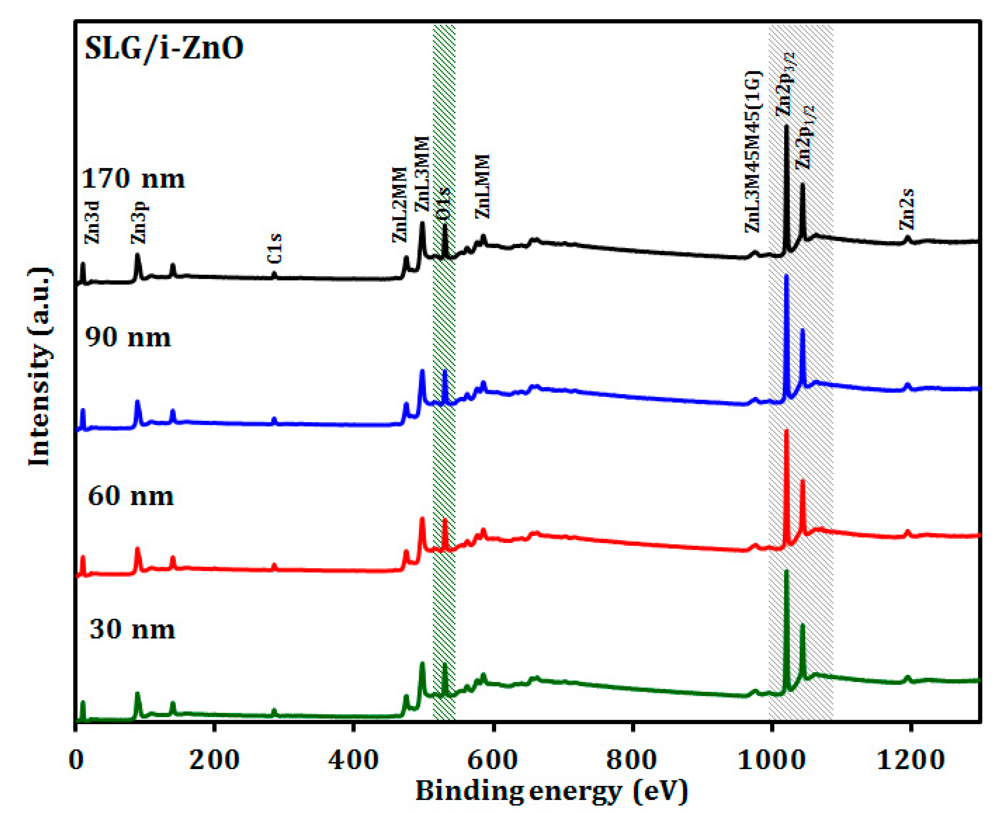
3.1. Microstructure and Morphology
3.2. Optical Properties
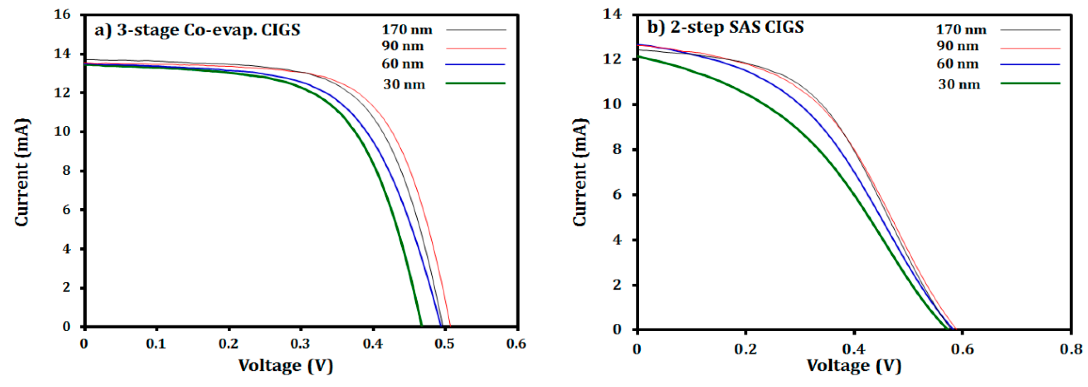
3.3. Influence of the i-ZnO Thickness on the CIGS Solar Cell Performance
4. Conclusions
Author Contributions
Funding
Conflicts of Interest
References
- Osborne, M. First Solar Building New 1.2GW CdTe Thin-Film Manufacturing Plant in Perrysburg. Available online: https://www.pv-tech.org/news/first-solar-building-new-1.2gw-cdte-thin-film-manufacturing-plant-in-perrys (accessed on 26 February 2018).
- Solar Frontier. Available online: http://www.solar-frontier.com/eng/index.html (accessed on 1 Febraury 2019).
- Colthorpe, A. Solar Frontier Achieves CIS Thin-Film Lab Efficiency Record of 23.35%. Available online: https://www.pv-tech.org/news/solar-frontier-achieves-cis-thin-film-efficiency-record-of-23.35 (accessed on 1 Febraury 2019).
- Glopal Solar. Available online: http://www.globalsolar.com/ (accessed on 1 Febraury 2019).
- Powalla, M.; Paetel, S.; Hariskos, D.; Wuerz, R.; Kessler, F.; Lechner, P.; Wischmann, W.; Friedlmeier, T.M. Advances in cost-ffficient thin-film photovoltaics based on Cu(In,Ga)Se2. Engineering 2017, 3, 445–451. [Google Scholar] [CrossRef]
- Ramanujam, J.; Singh, U.P. Copper indium gallium selenide based solar cells—A review. Energy Environ. Sci. 2017, 10, 1306–1319. [Google Scholar] [CrossRef]
- Yeh, M.-H.; Ho, S.-J.; Chen, G.-H.; Yeh, C.-W.; Chen, P.-R.; Chen, H.-S. Toward low-cost large-area CIGS thin film III: Effect of Se concentration on crystal growth and defect formation of sequentially electrodeposited CIGS thin films. Sol. Energy 2016, 132, 547–557. [Google Scholar] [CrossRef]
- Jackson, P.; Wuerz, R.; Hariskos, D.; Lotter, E.; Witte, W.; Powalla, M. Effects of heavy alkali elements in Cu(In,Ga)Se2 solar cells with efficiencies up to 22.6%. Phys. Status Solidi-Rapid Res. Lett. 2016, 10, 583–586. [Google Scholar] [CrossRef]
- Luo, S.; Lee, J.-H.; Liu, C.-W.; Shieh, J.-M.; Shen, C.-H.; Wu, T.-T.; Jang, D.; Greer, J.R. Strength, stiffness, and microstructure of Cu(In,Ga)Se2 thin films deposited via sputtering and co-evaporation. Appl. Phys. Lett. 2014, 105, 11907. [Google Scholar] [CrossRef]
- Langhorst, M.; Bykov, E.; Jiang, Q.; Kim, J.; Rozeveld, S.; Mushrush, M.; Wall, A.; Khare, A.; Feist, R. Control of CIGS roughness by initial selenization temperature. In Proceedings of the 2015 IEEE 42nd Photovolt. Spec. Conf. (PVSC 42), New Orleans, LA, USA, 14–19 June 2015. [Google Scholar] [CrossRef]
- Kim, S.T.; Kim, K.; Yun, J.H.; Ahn, B.T. A new simple route to grow Cu(In,Ga)Se2 thin films with large grains in the co-evaporation process. Appl. Phys. 2018, 18, 912–918. [Google Scholar]
- Lee, D.; Yong, K. Non-vacuum deposition of CIGS absorber films for low-cost thin film solar cells. Korean J. Chem. Eng. 2013, 30, 1347–1358. [Google Scholar] [CrossRef]
- Misic, B.; Pieters, B.E.; Theisen, J.P.; Gerber, A.; Rau, U. Shunt mitigation in ZnO:Al/i-ZnO/CdS/Cu(In,Ga)Se2 solar modules by the i-ZnO/CdS buffer combination. Phys. Status Solidi. 2015, 212, 541–546. [Google Scholar] [CrossRef]
- Williams, B.L.; Zardetto, V.; Kniknie, B.; Verheijen, M.A.; Kessels, W.M.; Creatore, M. The competing roles of i-ZnO in Cu(In,Ga)Se2 solar cells. Sol. Energy Mater. Sol. Cells 2016, 157, 798–807. [Google Scholar] [CrossRef]
- Williams, B.L.; Smit, S.; Kniknie, B.J.; Bakker, K.J.; Keuning, W.; Kessels, W.M.M.; Schropp, R.E.I.; Creatore, M. Identifying parasitic current pathways in CIGS solar cells by modelling dark J-Vresponse. Prog. Photovolt. Appl. 2015, 23, 1516–1525. [Google Scholar] [CrossRef]
- Nagoya, Y.; Sang, B.; Fujiwara, Y.; Kushiya, K.; Yamase, O. Improved performance of Cu(In,Ga)Se-based submodules with a stacked structure of ZnO window prepared by sputtering. Sol. Energy Mater. Sol. Cells 2003, 75, 163–169. [Google Scholar] [CrossRef]
- Bosio, A.; Romeo, N.; Mazzamuto, S.; Canevari, V. Polycrystalline CdTe thin films for photovoltaic applications. Prog. Cryst. Growth Charact. Mater. 2006, 52, 247–279. [Google Scholar] [CrossRef]
- Weinhardt, L.; Heske, C.; Niesen, T.P.; Karg, F.; Umbach, E.; Visbeck, S. Band alignment at the i- ZnO/CdS interface in Cu(In,Ga)(S,Se)2 thin-film solar cells. Appl. Phys. Lett. 2004, 84, 3175. [Google Scholar] [CrossRef]
- Chirilă, A.; Pianezzi, F.; Bloesch, P.; Gretener, C.; Sutter-Fella, C.; Kranz, L.; Perrenoud, J.; Verma, R.; Nishiwaki, S.; Bilger, G.; et al. Highly efficient Cu(In,Ga)Se2 solar cells grown on flexible polymer films. Nat. Mater. 2011, 10, 857–861. [Google Scholar] [CrossRef]
- Herrmann, D.; Kratzert, P.; Weeke, S.; Zimmer, M.; Djordjevic-Reiss, J.; Hunger, R.; Lindberg, P.; Wallin, E.; Lundberg, O.; Stolt, L. CIGS module manufacturing with high deposition rates and efficiencies. In Proceedings of the 2014 IEEE 40th Photovolt. Spec. Conf. (PVSC 40), Denver, CO, USA, 8–13 June 2014. [Google Scholar] [CrossRef]
- Lindahl, J.; Zimmermann, U.; Szaniawski, P.; Torndahl, T.; Hultqvist, A.; Salome, P.; Platzer-Bjorkman, C.; Edoff, M. Inline Cu(In,Ga)Se2 co-evaporation for high-efficiency solar cells and modules. IEEE J. Photovolt. 2013, 3, 1100–1105. [Google Scholar] [CrossRef]
- Löckinger, J.; Nishiwaki, S.; Andres, C.; Erni, R.; Rossell, M.D.; Romanyuk, Y.E.; Buecheler, S.; Tiwari, A.N. ALD-ZnxTiyO as window layer in Cu(In,Ga)Se2 solar cells. ACS Appl. Mater. Interfaces 2018, 10, 43603–43609. [Google Scholar] [CrossRef]
- Zortea, L.; Nishiwaki, S.; Weiss, T.P.; Haass, S.; Perrenoud, J.; Greuter, L.; Feurer, T.; Palaniswamy, G.; Buecheler, S.; Tiwari, A.N. Cu(In,Ga)Se2 solar cells on low cost mild steel substrates. Sol. Energy 2018, 175, 25–30. [Google Scholar] [CrossRef]
- Broussillou, C.; Viscogliosi, C.; Rogee, A.; Angle, S.; Grand, P.P.; Bodnar, S.; Debauche, C.; Allary, J.L.; Bertrand, B.; Guillou, C.; et al. Statistical process control for Cu(In,Ga)(S,Se)2 electrodeposition-based manufacturing process of 60 × 120 cm2 modules up to 14,0% efficiency. In Proceedings of the 2015 IEEE 42nd Photovolt. Spec. Conf. (PVSC 42), New Orleans, LA, USA, 14–19 June 2015. [Google Scholar] [CrossRef]
- Todorov, T.K.; Gunawan, O.; Gokmen, T.; Mitzi, D.B. Solution-processed Cu(In,Ga)(S,Se)2 absorber yielding a 15.2% efficient solar cell. Prog. Photovolt. Res. Appl. 2013, 21, 82–87. [Google Scholar] [CrossRef]
- Bhattacharya, R.N. CIGS-based solar cells prepared from electrodeposited stacked Cu/In/Ga layers. Sol. Energy Mater. Sol. Cells 2013, 113, 96–99. [Google Scholar] [CrossRef]
- Mansfield, L.M.; Noufi, R.; Muzzillo, C.P.; Dehart, C.; Bowers, K.; To, B.; Pankow, J.W.; Reedy, R.C.; Ramanathan, K. Enhanced performance in Cu(In,Ga)Se2 solar cells fabricated by the two-step selenization process With a Potassium Fluoride Postdeposition Treatment. IEEE J. Photovolt. 2014, 4, 1650–1654. [Google Scholar] [CrossRef]
- Kato, T.; Handa, A.; Yagioka, T.; Matsuura, T.; Yamamoto, K.; Higashi, S.; Wu, J.-L.; Tai, K.F.; Hiroi, H.; Yoshiyama, T.; et al. Enhanced efficiency of Cd-free Cu(In,Ga)(Se,S)2 minimodule via (Zn,Mg)O second buffer layer and alkali metal post-treatment. IEEE J. Photovolt. 2017, 7, 1773–1780. [Google Scholar] [CrossRef]
- Alhammadi, S.; Moon, K.; Park, H.; Kim, W.K.; Salh, A. Effect of different cadmium salts on the properties of chemical-bath-deposited CdS thin films and Cu(InGa)Se2 solar cells. Thin Solid Films 2017, 625, 56–61. [Google Scholar] [CrossRef]
- Kodigala, S.R. Cu(In1-xGax)Se2 Based Thin Film Solar Cells, 1st ed.; Academic Press: Burlington, NJ, USA, 2010; pp. 001–700. [Google Scholar]
- Jahagirdar, A.H.; Kadam, A.A.; Dhere, N.G. Role of i-ZnO in optimizing open circuit voltage of CIGS2 and CIGS thin film solar cells. In Proceedings of the 2006 IEEE 4th World Conf. Photovolt. Energy Conf. (WCPEC–4), Waikoloa, HI, USA, 7–12 May 2006. [Google Scholar] [CrossRef]
- National Fach Informationszentrum (FIZ) Karlsruhe. Inorganic Crystal Structure Database (ICSD). Available online: https://www.fiz-karlsruhe.de/en/produkte-und-dienstleistungen/inorganic-crystal-structure-database-icsd (accessed on 1 Febraury 2019).
- Hahn, Y.-B. Zinc oxide nanostructures and their applications. Korean J. Chem. Eng. 2011, 28, 1797–1813. [Google Scholar] [CrossRef]
- Li, B.Y.; Zhang, Y.; Wang, H.; Wang, B.; Wu, L.; Sun, Y. Preferred orientation of Cu(In,Ga)Se2 thin film deposited on stainless steel substrate. Prog. Photovolt. Res. Appl. 2013, 21, 838–848. [Google Scholar]
- Chaisitsak, S.; Yamada, A.; Konagai, M. Preferred orientation control of Cu(In1-xGax)Se2(x≈0.28) thin films and its influence on solar cell characteristics. Jpn. J. Appl. Phys. 2002, 41, 507–513. [Google Scholar] [CrossRef]
- Yan, Y.; Jiang, F.; Liu, L.; Yu, Z.; Zhang, Y.; Zhao, Y. Control over the preferred orientation of CIGS films deposited by magnetron sputtering using a wetting layer. Electron. Mater. Lett. 2016, 12, 59–66. [Google Scholar] [CrossRef]
- Londhe, P.U.; Rohom, A.B.; Fernandes, R.; Chaure, N.B.; Kothari, D.C. Development of superstrate CuInGaSe2 thin film solar cells with low-cost electrochemical route from nonaqueous bath. ACS Sustain. Chem. Eng. 2018, 6, 4987–4995. [Google Scholar] [CrossRef]
- Koo, J.; Kwon, S.; Roh, Y.-S.; Lee, S.-J.; Jung, K.-Y.; Shafarman, W.N.; Park, J.-H.; Kim, D.H.; Myoung, J.-M. Effect of reaction temperature and time during two-step selenization and sulfurization of Se-coated CuGa/In precursors. Electron. Mater. Lett. 2016, 12, 484–493. [Google Scholar] [CrossRef]
- Moon, K.; Kim, W.K. Cu(InGa)Se2 absorber formation by in-situ, low-temperature annealing of co-evaporated bilayer (InGa)2Se3/CuSe precursors. Thin Soilds Films 2015, 596, 63–67. [Google Scholar] [CrossRef]
- Lu, C.J.; Kuang, A.X.; Huang, G.Y.; Wang, S.M. XPS study on composition and structure of epitaxial KTa1-xNbxO3 (KTN) thin films prepared by the sol-gel process. J. Mater. Sci. 1996, 31, 3081–3085. [Google Scholar] [CrossRef]
- Rana, A.K.; Das, R.; Kumar, Y.; Sen, S.; Shirage, P.M. Growth of transparent Zn1−xSrxO (0.0≤x≤0.08) films by facile wet chemical method: Effect of Sr doping on the structural, optical and sensing properties. Appl. Surf. Sci. 2016, 379, 23–32. [Google Scholar] [CrossRef]
- Singh, S.; Chakrabarti, P. Comparison of the structural and optical properties of ZnO thin films deposited by three different methods for optoelectronic applications. Superlattices Microstruct. 2013, 64, 283–293. [Google Scholar] [CrossRef]
- Sehar, S.; Naz, I.; Perveen, I.; Ahmed, S. Superior dye degradation using SnO2-ZnO hybrid heterostructure catalysts. Korean J. Chem. Eng. 2019, 36, 56–62. [Google Scholar] [CrossRef]
- Gu, Z.-B.; Lu, M.-H.; Wang, J.; Wu, D.; Zhang, S.-T.; Meng, X.-K.; Zhu, Y.-Y.; Zhu, S.-N.; Chen, Y.-F.; Pan, X.-Q. Structure, optical, and magnetic properties of sputtered manganese and nitrogen-codoped ZnO films. Appl. Phys. Lett. 2006, 88, 82111. [Google Scholar] [CrossRef]
- Hsieh, P.-T.; Chen, Y.-C.; Kao, K.-S.; Wang, C.-M. Luminescence mechanism of ZnO thin film investigated by XPS measurement. Appl. Phys. A 2007, 90, 317–321. [Google Scholar] [CrossRef]
- Sun, X.; Wang, L.; Kwok, H.S. Improved ITO thin films with a thin ZnO buffer layer by sputtering. Thin Solid Films 2000, 360, 75–81. [Google Scholar] [CrossRef]
- Karasawa, T.; Miyata, Y. Electrical and optical properties of indium tin oxide thin films deposited on unheated substrates by d.c. reactive sputtering. Thin Solid Films 1993, 223, 135–139. [Google Scholar] [CrossRef]
- Kim, H.; Horwitz, J.S.; Kushto, G.; Piqué, A.; Kafafi, Z.H.; Gilmore, C.M.; Chrisey, D.B. Effect of film thickness on the properties of indium tin oxide thin films. J. Appl. Phys. 2000, 88, 6021–6025. [Google Scholar] [CrossRef]
- Huang, C.-H.; Chuang, W.-J.; Lin, C.-P.; Jan, Y.-L.; Shih, Y.-C. Deposition Technologies of High-Efficiency CIGS Solar Cells: Development of Two-Step and Co-Evaporation Processes. Crystals 2018, 8, 296. [Google Scholar] [CrossRef]
- Vasekar, P.S.; Dhere, N.G.; Moutinho, H. Development of CIGS2 solar cells with lower absorber thickness. Sol. Energy 2009, 83, 1566–1570. [Google Scholar] [CrossRef]
- Dongaonkar, S.; Servaites, J.D.; Ford, G.M.; Löser, S.; Moore, J.; Gelfand, R.M.; Mohseni, H.; Hillhouse, H.W.; Agrawal, R.; Ratner, M.A.; et al. Universality of non-Ohmic shunt leakage in thin-film solar cells. J. Appl. Phys. 2010, 108, 124509. [Google Scholar] [CrossRef]
- Manthina, V.; Agrios, A.G. Single-pot ZnO nanostructure synthesis by chemical bath deposition and their applications. Nano-Struct. Nano-Objects 2016, 7, 1–11. [Google Scholar] [CrossRef]


| Organization | Substrate | Absorber Preparation Method | i-ZnO Thickness (nm) | Conversion Efficiency (%) | Note | Reference |
|---|---|---|---|---|---|---|
| ZSW | Glass | Co-evaporation | 50–100 | 22.6 | [8] | |
| Solibro GmbH | Glass | 50 | 14.4 | [20] | ||
| Uppsala | Glass | 70 | 18.6 | [21] | ||
| EMPA | Glass | 80 | 20.7 | [22] | ||
| Steel | 50 | 18 | Flexible mild steel | [23] | ||
| polyimide (PI) | 50–100 | 18.7 | FlexiblePI | [19] | ||
| Nexcis | Glass | Electrodeposition and atmospheric annealing | 80 | 17.3 | [24] | |
| IBM | Glass | Solution and spin coating | 80 | 15.2 | Hydrazine-based solution | [25] |
| NREL | Glass | Electrodeposition and selenization (CIGSe) | 60 | 11.7 | [26] | |
| Glass | Evaporation and selenization | 50 | 18.6 | [27] | ||
| Solar Frontier | Glass | Metal sputtering + Sulfurization after selenization | 100–200 | 18.6 | Mini module | [28] |
| Growth Process of CIGS | i-ZnO Thickness (nm) | Solar Cell Performance Parameters | |||||
|---|---|---|---|---|---|---|---|
| JSC (mA/cm2) | VOC (V) | FF (%) | Efficiency (%) | RSH (Ω cm2) | RS (Ω cm2) | ||
| Three-stage co-evap. | 30 | 34.9 | 0.467 | 61.8 | 10.1 | 529.6 | 7.24 |
| 60 | 35.1 | 0.494 | 61.0 | 10.6 | 617.8 | 8.26 | |
| 90 | 35.2 | 0.507 | 66.3 | 11.8 | 1127 | 6.54 | |
| 170 | 34.0 | 0.495 | 63.3 | 10.7 | 864.5 | 7.66 | |
| Two-step SAS | 30 | 31.6 | 0.574 | 38.5 | 6.96 | 129.7 | 31.0 |
| 60 | 32.9 | 0.580 | 41.5 | 7.97 | 182.7 | 28.4 | |
| 90 | 32.8 | 0.590 | 45.2 | 8.75 | 254.0 | 25.6 | |
| 170 | 32.3 | 0.580 | 47.4 | 8.87 | 370.6 | 24.3 | |
© 2019 by the authors. Licensee MDPI, Basel, Switzerland. This article is an open access article distributed under the terms and conditions of the Creative Commons Attribution (CC BY) license (http://creativecommons.org/licenses/by/4.0/).
Share and Cite
Alhammadi, S.; Park, H.; Kim, W.K. Optimization of Intrinsic ZnO Thickness in Cu(In,Ga)Se2-Based Thin Film Solar Cells. Materials 2019, 12, 1365. https://doi.org/10.3390/ma12091365
Alhammadi S, Park H, Kim WK. Optimization of Intrinsic ZnO Thickness in Cu(In,Ga)Se2-Based Thin Film Solar Cells. Materials. 2019; 12(9):1365. https://doi.org/10.3390/ma12091365
Chicago/Turabian StyleAlhammadi, Salh, Hyeonwook Park, and Woo Kyoung Kim. 2019. "Optimization of Intrinsic ZnO Thickness in Cu(In,Ga)Se2-Based Thin Film Solar Cells" Materials 12, no. 9: 1365. https://doi.org/10.3390/ma12091365
APA StyleAlhammadi, S., Park, H., & Kim, W. K. (2019). Optimization of Intrinsic ZnO Thickness in Cu(In,Ga)Se2-Based Thin Film Solar Cells. Materials, 12(9), 1365. https://doi.org/10.3390/ma12091365