Article

Mode Conversion of the Edge Modes in the Graphene Double-Ribbon Bend

1
Department Medical Technology and Engineering, Henan University of Science and Technology, Luoyang 471000, China
2
Jiangsu Provincial Research Center of Light Industrial Optoelectronic Engineering and Technology, Jiangnan University, Wuxi 214122, China
*
Author to whom correspondence should be addressed.
Materials 2019, 12(23), 4008; https://doi.org/10.3390/ma12234008
Submission received: 5 October 2019 / Revised: 22 November 2019 / Accepted: 24 November 2019 / Published: 3 December 2019
(This article belongs to the Section Optical and Photonic Materials)

Abstract

:
In this paper, a new kind of graphene double-ribbon bend structure, which can support two edge graphene surface plasmons (EGSPs) modes, is proposed. In this double-ribbon bend, one edge mode can be partly converted into another one. We attribute the mode conversion mechanism to the interference between the two edge plasmonic modes. Based on the finite element method (FEM), we calculate the transmission and loss of EGSPs propagating along this graphene double-ribbon bend in the mid-infrared range under different parameters.

1. Introduction

Graphene, due to its unique mechanical, electrical and optical properties [1,2,3,4], is a promising candidate for nanoscale photonic applications in infrared frequencies. Surface plasmons (SPs) supported by graphene has recently attracted intensive attention driven by maturing state-of-the-art nanofabrication technology. Compared to SPs in noble metals, graphene surface plasmons (GSPs) exhibit even stronger mode confinement and relatively longer propagation distance, with an additional unique ability to be tunable by adjusting gate voltage or chemical doping concentration [5,6,7,8,9]. GSPs brings many unique phenomena such as negative refraction [10,11], cloaking [12,13], and superlens [14,15]. Its extraordinary features are applied to a series of optical devices such as absorbers [16,17], modulators [18,19,20], and sensors [21,22].
The graphene ribbons can support both waveguide GSPs (WGSPs) modes and strongly confined edge GSPs (EGSPs) modes. EGSPs are the fundamental modes, which are strongly localized along the graphene edge, show a larger effective refractive index and stronger field confinement [23]. EGSPs modes are firstly observed experimentally in a patterned graphene nanoribbon on Al2O3 substrates [24]. The width of the graphene ribbon is inversely proportional to the wave vectors of EGSPs and EGSPs modes show cut-off behavior [25]. Conventional straight ribbon waveguides, including multilayer nano-ribbon [26], ribbon resonators with rings [27] and wrings [28], are studied in detail. A graphene bending ribbon waveguide is proposed to explore the spatial coupling between the edge modes [29]. Furthermore, edge modes supported by bending ribbon waveguide spatially split with the strongly confined symmetric (anti-symmetric) mode, which shifts to the exterior (interior) edge of the incidence [30].
In the paper, we propose a new kind of double-ribbon bend that supports two EGSPs. Based on the finite element method (FEM), we firstly discuss the dispersion relation of EGSPs for this double-ribbon bend. We calculate transmission and loss of edge modes with different bending angles under Fermi level, separation distance, incidence wavelength, bending radius and double-ribbon width. The mode conversion is due to interference between the two EGSPs, and the loss of double-ribbon originates from the absorption loss and bending loss. The period of the mode conversion by simulation is in accordance with the theoretical results.

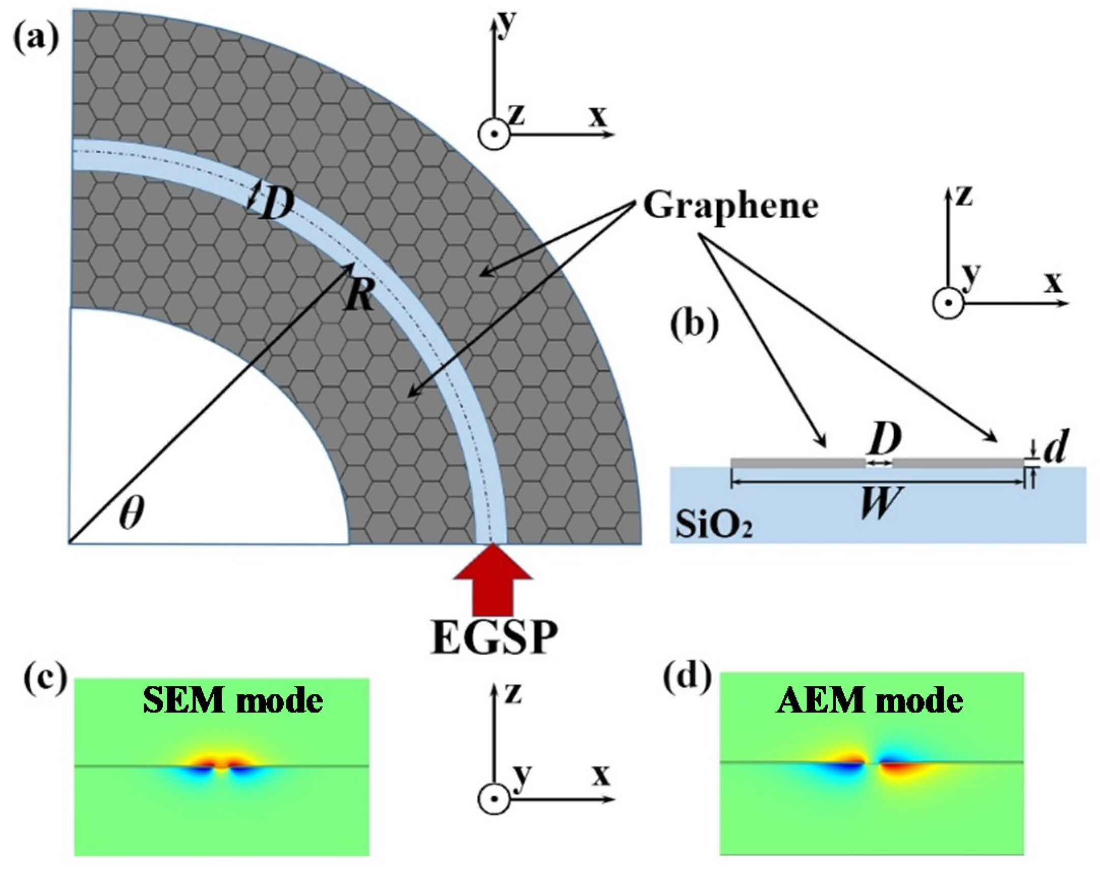
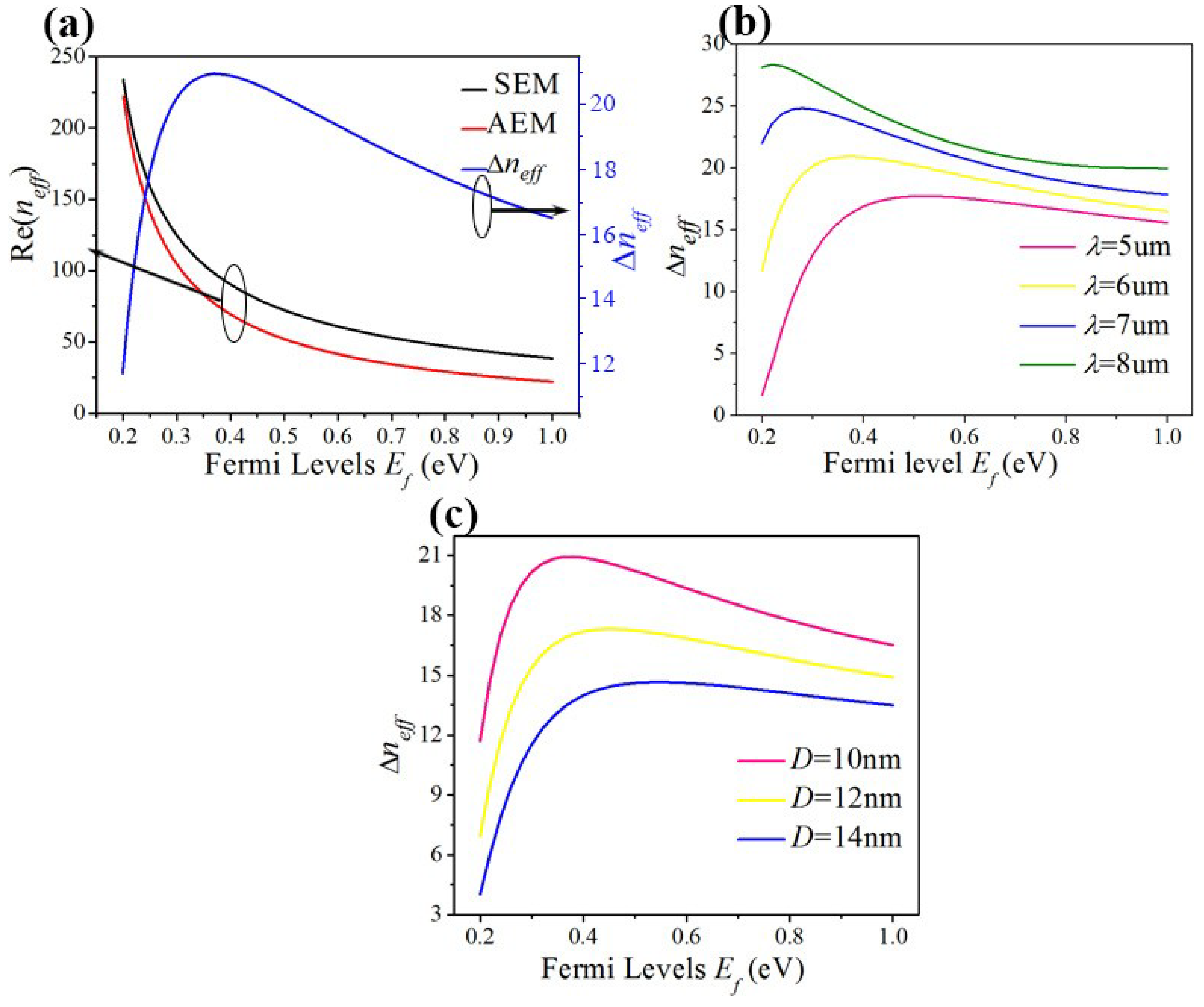
2. Structure and EGSPs Dispersion

The SPs supported by individual graphene nano-ribbons has been discussed very frequently. Plasmon interaction and hybridization in pairs of neighboring aligned ribbons are shown to be strong enough to produce dramatic modifications in the plasmon field profiles [31]. What will happen if there are two paralleled bending ribbons? Inspired by these edge modes study, we propose a new kind of bend structure with two paralleled graphene ribbons with an interval of D. When the two edges of two ribbons come closer to each other, they will bring out two of edge modes with opposite parity [31].
As illustrated in Figure 1a, a pair of paralleled graphene ribbon bends with a separation interval of D is deposited on the SiO2 substrate, and these two bending ribbons are of equal width. Figure 1b is the sectional view of Figure 1a. The dielectric above is air. The relative dielectric constant of SiO2 substrate is 2.25. The radius and the width of the double-ribbon bend are R and W, respectively. The thickness of the graphene double-ribbon bend is 1 nm. The bending angle of the structure is denoted by θ. Here, we only discuss the condition when D is smaller than 20 nm, where the ribbons structure supports the two EGSPs modes.
As is known, there is only one edge mode in a semi-infinite graphene sheet. When two semi-infinite paralleled graphene sheets are closed to each other, the two semi-infinite edge modes will be mutually coupled into two edge modes. Here, as width of the bending ribbon structure is much bigger than separation distance (W >> D), we can consider the two graphene ribbons as two semi-infinite sheets, and the coupling happens at the internal edge of the double-ribbon bend (near the blue region showing in Figure 1a). Here, the surface conductivity of graphene, σG, is obtained using the Kubo formula [32]
σ G = i e 2 E f π 2 ( ω + i τ 1 ) + i e 2 4 π I n [ 2 E f ( ω + i τ 1 ) 2 E f + ( ω + i τ 1 ) ] + i e 2 k B T π 2 ( ω + i τ 1 ) In [ exp ( E f k B T ) + 1 ]
In Equation (1), ħ, e and kB represent reduced Planck’s constant, the electron charge and Boltzmann’s constant respectively. Equation (1) shows that σG depends on the Fermi levels Ef, the momentum relaxation time τ, temperature T, and the photon frequency ω. Fermi energy level is shown in Equation (2)
E f = V f ( π n ) 1 / 2
where n is the charge carrier concentration, the Fermi velocity Vf is 106 m/s. The permittivity εG of graphene is governed by
ε G = 1 + i σ G η 0 k 0 d
where η0 (≈377 Ω) is the impedance of air, τ is chosen as 0.5 ps, the thickness of graphene d is 1 nm, and the temperature T = 300 K. Due to graphene’s particular characteristics, εG can be tuned by modifying the gate voltage or doped by chemical doping.
We choose COMSOL Multiphysics based on the finite element method (FEM) to conduct modes analysis of GESPs mode for our double-ribbon bend and all simulation in the paper will be conducted by FEM [28]. Figure 1c,d plot GESP modes’ z-component of magnetic field in the x-z plane, when the incident wavelength is 6 μm, Ef = 0.2 eV, D = 10 nm and W = 200 nm. Z-component of magnetic field in Figure 1c is symmetrical, which can illustrate the symmetric EGSPs mode (SEM); and that of Figure 1d is anti-symmetrical, which can illustrate the anti-symmetric EGSPs mode (AEM).
The differences between the real parts of effective refractive indexes for the two edge modes can be obtained by
Δ n e f f = Re ( n 1 ) Re ( n 2 )
In Equation (4), Re(n1) and Re(n2) represent the real part of two EGSPs’ effective refractive index respectively. Figure 2 shows the dispersion relation of the two EGSPs’ modes. It implies that Re (n1), Re (n2), and Δneff is related to the following parameters: Fermi levels Ef, wavelengths λ, and separation distance D. Figure 2a shows the real parts of the effective refractive index (Re(neff)) of the SEM (black line) and AEM (red line) mode both decrease with increasing Ef; but the exact opposite is for the difference Δneff between two EGSPs’ modes (blue line), when λ = 6 μm and D = 10 nm. As can be seen in Figure 2b, when the incident wavelengths are 5, 6, 7, and 8 μm (plotted in pink, yellow, blue, and green lines) respectively, Δneff firstly rises then decreases with increasing Fermi level Ef under the same wavelength. And the Δneff is larger when λ is increasing from 5 to 8 μm under the same Ef. Figure 2c shows when separation distance D = 10, 12 and 14 nm (plotted in pink, yellow and blue lines), Δneff firstly rises then decreases with increasing Fermi level Ef under the same separation distance D. The Δneff is larger when D is decreasing from 14 to 10 μm under the same Ef.

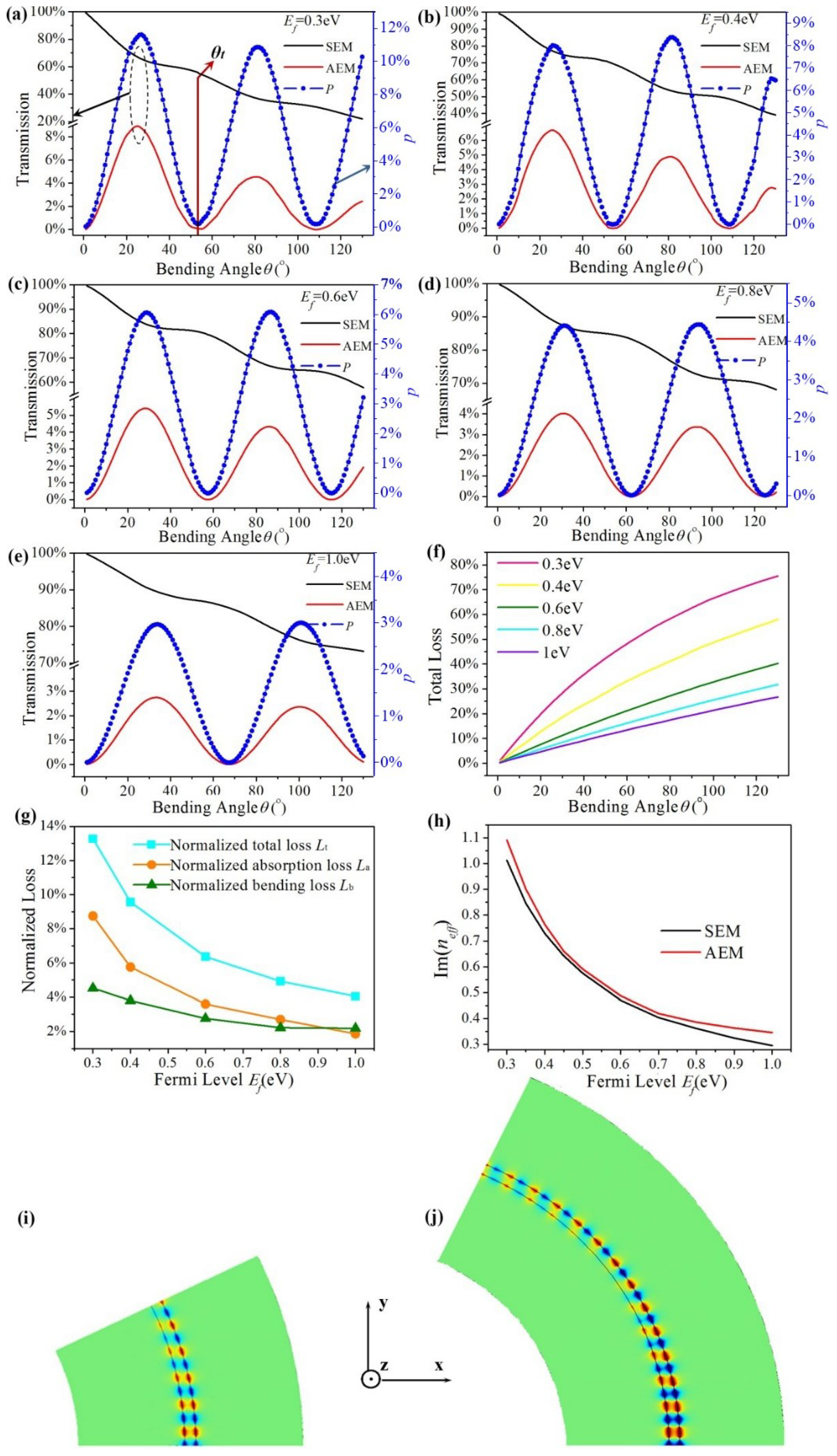
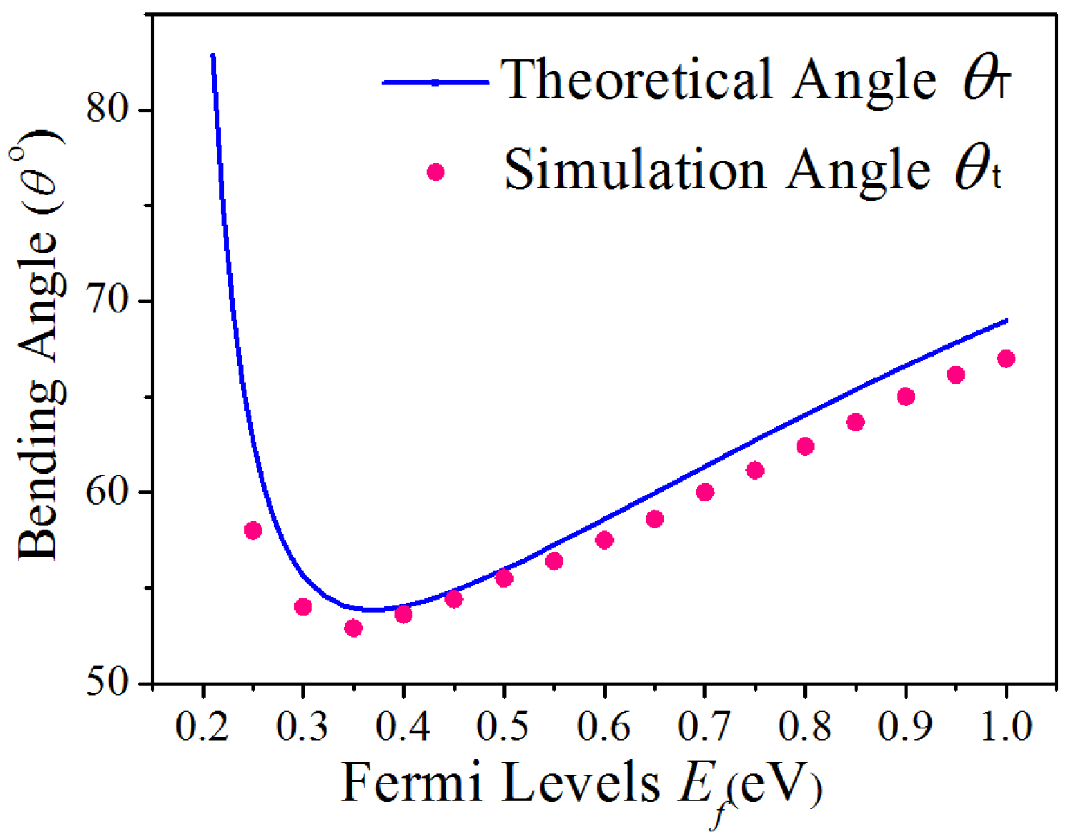
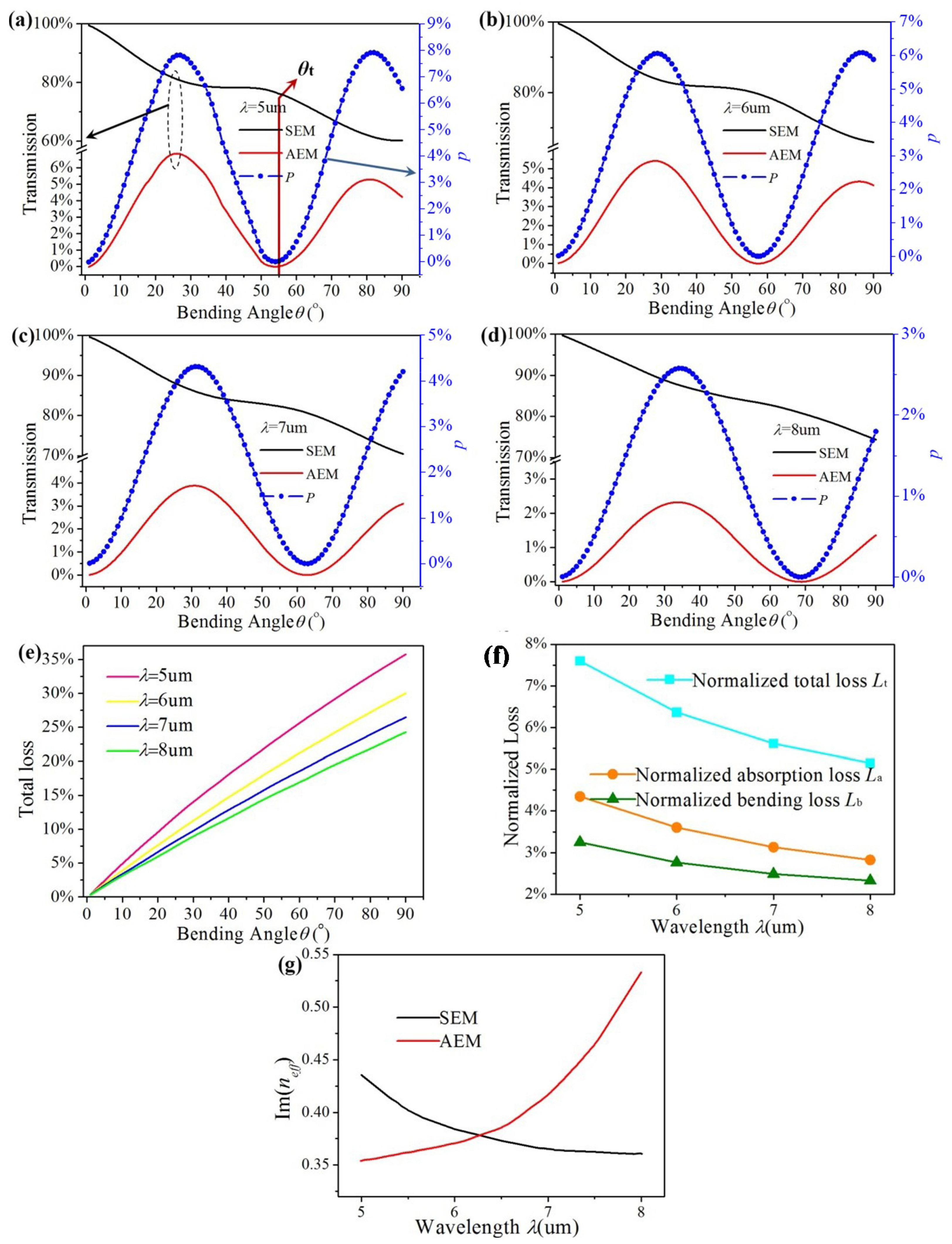
3. Mode Conversion and Simulations Results

Due to the interference between the SEM and AEM mode, mode conversion happens when one mode is propagating along with our proposed structure. We define a periodic variation angle θT, which is used to analyze the interference process between the SEM and AEM [30,33,34]. The positive integer k represents the order of the conversion period
2 θ T R Δ n e f f = k λ ( k = 1 , 2 , 3 )
To further investigate the mode conversion mechanism between two EGSPs, we calculate bending loss, total losses and the mode distribution, under different bending angles θ, Fermi levels Ef, separation distances D, wavelengths λ, and bending radii R, respectively. Here, the SEM is coupled into the bottom port of the double-ribbon bend as shown in Figure 1a, and propagates along the two ribbons structure. The initial parameters are: D = 10 nm, R = 300 nm, λ = 6 μm and W = 200 nm. We define the conversion efficiency P, which represents the ratio between the transmission of the converted mode and the total transmission at the output
P = T 2 T 1 + T 2
where T1 and T2 represent the transmission of SEM and AEM in respectively. P reaches the maximum, which means conversion efficiency between SEM and AEM is highest, and P reaches minimum, which means SEM propagates along our proposed structure without mode conversion.
Figure 3 shows the periodic conversion between two EGSPs’ modes under different Fermi levels (Ef = 0.3, 0.4, 0.6, 0.8, and 1 eV). The SEM’s transmission is plotted in the black line and AEM’s is in the red line. The blue ones represent the conversion efficiency P, in Figure 3a–e. It is found that SEM is partly converted to AEM with different bending angles (ranging from 0° to 130°). The mode conversion happens due to the interference between the SEM and AEM. The three lines have the same change periods with a bending angle under the same Ef. The variation amplitude of SEM’s declines with bending angle, but those of AEM and P are nearly unchanged. θt is the conversion period, when the bending angle is θt/2, P reaches the maximum; and when the bending angle is θt, P reaches the minimum. It is found that when Ef is 0.3, 0.4, 0.6, 0.8, and 1 eV, θt is 54.6°, 54°, 57.8°, 62.4°, and 67° respectively, which is accordance with Equation (5). The theoretical value θT of the conversion period is 54.5°, 54.8°, 58.6°, 64°, and 69°, respectively. The maximum of conversion efficiency P is 15.40%, 13.92%, 11.86%, 8.68%, and 5.80%, respectively, and the conversion efficiency P decreases with increasing Ef.
Because of graphene absorption loss and bending radiation loss, SEM’s transmission decreases gradually. Here, we define the total losses LT, which is calculated by
L T = 1 T 1 T 2 R 1 R 2
where R1 and R2 are the reflectivity of SEM and AEM for our proposed structure. LT consists of absorption loss and bending loss. Here, we define this absorption loss of per unit length for a straight double-ribbon waveguide as normalized absorption loss La. The normalized total loss Lt is derived from the total loss LT over the actual propagation length (i.e., the center arc length of this double-ribbon). The normalized bending loss Lb is defined by the difference between Lt and La.
Figure 3f shows the total loss LT vs. bending angle under different fermi levels. LT increases with increasing bending angles under the same Ef, because larger bending angles mean larger propagation loss of EGSPs. LT decreases with increasing Ef under the same bending angles. The three normalized losses Lt, La and Lb are plotted by cyan, orange, and olive lines respectively in Figure 3g, they all decrease with increasing Ef. Figure 3h shows the imaginary parts of the effective refractive index for SEM and AEM are almost the same, and Im(neff) decreases with increasing Ef for both SEM and AEM. Larger Im(neff) causes a bigger normalized absorption loss La, which can explain that La decreases with increasing Ef in Figure 3h. When bending angels are 27.3° and 54.5°, the magnetic field distributions Hz are shown in Figure 3i,j under Ef = 0.3 eV. It is found that when bending angle is 27.3°, SEM can be partly converted into AEM (P = 15.40%), so magnetic field distributions Hz at the output is the superposition of AEM and SEM; when bending angle is 54.5°, SEM can propagate through the bending structure without mode conversion, so magnetic field distributions Hz at the output is symmetrical.
The solid line and dashed line represent the theoretical value θT and simulation value θt for conversion period respectively, under different Ef, in Figure 4. The conversion period firstly decreases and then increases with increasing Ef. It is found that the theoretical value θT matches very well with the simulation results.
Periodical mode conversion between SEM and AEM under different separation distances (D = 10, 12, and 14 nm) is shown in Figure 5a–c. Other parameters are as follows: Ef = 0.6 eV, R = 300 nm, λ = 6 μm, and W = 200 nm. It is also found that SEM is partly converted to AEM varying with different bending angles. The transmission of two EGSPs and P both have the same changing period with bending angle (ranging from 0° to 90°) under the same D when D is 10, 12, and 14 nm, θt is 58°, 65.7°, and 74°. The theoretical value θT, which is obtained by Equation (5), is 59.2°, 68.0°, and 78.4°. θt decreases with increasing D. That is because Δneff increases with increasing D under the same Ef in Figure 2b. Meanwhile, the maximum conversion efficiency Pmax respectively are 6.1%, 9.2%, and 13.5%, and increases with increasing D.
As illustrated in Figure 5d, the total loss LT is plotted in red, green, and blue lines when the separation distance D is chosen as 10, 12, and 14 nm. It is found that total loss LT increases with increasing bending angle under the same separation distance D, but LT is almost the same under the same bending angle. LT is a litter larger for smaller D, which is shown in the insert of Figure 5e. As shown in Figure 5e, the normalized loss Lt, La, and Lb are plotted in cyan, orange, and olive lines, respectively. Lt and La decrease a little with increasing D. Lb barely changed with it. The reason is that Im(neff) of SEM decreases slightly with increasing D, but the opposite is true for AEM, which is shown in Figure 5f. So the absorption loss of SEM decreases slightly with increasing D, but the opposite is true for AEM. The absorption loss mainly originates from SEM’s propagation loss. So when D is increasing, Lt, La and total loss LT decreased a little due to the absorption loss difference between SEM and AEM. The proposed double-ribbon bend has the same curvature under three separation distances D, so Lb is also the same.
As shown in Figure 6a–d, periodic conversion between two EGSPs also happens under different wavelengths (λ = 5, 6, 7 and 8 μm). Other parameters are as follows: Ef = 0.6 eV, D = 10 nm, R = 300 nm, and W = 200 nm. The transmission of two EGSPs and the conversion efficiency P both have the same change period with bending angles under the same wavelength. It is can be seen in Figure 6a–d that when the wavelength is λ = 5, 6, 7 and 8 μm, θt is 54.9°, 57.8°, 63.5°, and 69.1°. Theoretical value θT is 54.4°, 58.6°, 64.4° and 70.1° based on Equation (5). The maximum conversion efficiency Pmax is 15.40%, 11.86%, 8.40%, and 4.96%, respectively. As illustrated in Figure 6e, the total loss LT is plotted in pink, yellow, blue, and green lines when the wavelength is 5, 6, 7, and 8 μm, respectively. It is found that total loss LT enhances with increasing bending angle under the same wavelength λ because of the absorption loss of EGSPs. LT decreases with increasing wavelength λ under the same bending angle. As shown in Figure 6f, the normalized loss Lt, La and Lb are plotted in cyan, orange and olive lines, respectively. They all decrease with increasing λ. As shown in Figure 6g, Im(neff) of SEM decreases with increasing λ, AEM does just the opposite. It’s worth noting that the proportion of SEM is much larger than AEM’s, the downtrend for Im(neff) of SEM will play a dominating role in the absorption loss. Thus, La declines with increasing λ.
As shown in Figure 7a–d, periodical couplings between SEM and AEM are presented by four bending radii: 300, 400, 500, and 600 nm, respectively. Other parameters are as follows: Ef = 0.6 eV, D = 10 nm, λ = 6 μm, and W = 200 nm. The transmission of two EGSPs and the conversion efficiency share the same converting period. When R is 300, 400, 500 and 600 nm, θt is 57.8°, 43.3°, 35.0°, and 29.0°. The theoretical angel θT obtained by Equation (5) is 58.6°, 44.4°, 33.9°, and 29.6°. The maximum of conversion efficiency Pmax is 6.06%, 3.45%, 2.22%, and 1.55%, respectively.
Figure 7e shows that the total loss LT of the double-ribbon bend varying with different bending angles under different R: 300 nm (pink line), 400 nm (yellow line), 500 nm (blue line), and 600 nm (green line). LT increases not only with increasing bending angles under the same R, but also increases with increasing R under the same bending angle. Because a longer propagating length will be obtained by a larger bending angle under the same R and larger R under the same bending angle, so does the absorption loss. As can be seen in Figure 7f, the normalized loss Lt and Lb both decrease with increasing R, but the normalized loss La is nearly unchanged with R. Because the Ef, D, and λ is the same, Im(neff) of AEM and SEM is the same, the normalized absorption loss La is accordingly unchanged with R. Because a larger R has a smaller curvature and lower bending radiation loss, Lb decreases with increasing R and so does Lt. To improve the mode conversion, gain medium can be added to reduce the absorption loss [35].

4. Conclusions

In this paper, we propose a new kind of double-ribbon bend that supports two EGSPs and focus on the conversion between two EGSPs. Using FEM, we prove the period of the conversion between two EGSPs is determined by a separation distance, incidence wavelength, and bending radius, and the period of the conversion can be also tuned by the Fermi level. The mode conversion originates from the interference between the two edge plasmonic modes. The loss of double-ribbon bend consists of the absorption loss and bending loss, and the effects of parameters on loss are also discussed. Our double-ribbon bend may provide a new perspective to understand the conversion relationship between two EGSPs.

Author Contributions

Conceived the idea of mode conversion of the edge modes in the graphene ribbon, L.Z. and B.X.; performed numerical simulations, L.Z. and B.X.; writing—original draft preparation, L.Z. and B.X.; writing—review and editing, Y.W.

Funding

This work was sponsored by the National Natural Science Foundation of China (11404143), Returned Overseas Fund of the Ministry of Education of China (1144130201150080).

Conflicts of Interest

The authors declare no conflict of interest.

References

  1. Geim, A.K.; Novoselov, K.S. The rise of graphene. Nat. Mater. 2007, 6, 183–191. [Google Scholar] [CrossRef] [PubMed]
  2. Bonaccorso, F.; Sun, Z.; Hasan, T.; Ferrari, A.C. Graphene photonics and optoelectronics. Nat. Photonics 2010, 4, 611–622. [Google Scholar] [CrossRef] [Green Version]
  3. Emani, N.K.; Kildishev, A.V.; Shalaev, V.M.; Boltasseva, A. Graphene: A dynamic platform for electrical control of plasmonic resonance. Nanophotonics 2015, 4, 214–223. [Google Scholar] [CrossRef] [Green Version]
  4. Constant, T.J.; Hornett, S.M.; Chang, D.E.; Hendry, E. All-optical generation of surface plasmons in graphene. Nat. Phys. 2015, 12, 124–128. [Google Scholar] [CrossRef] [Green Version]
  5. Garcia de Abajo, F.J. Graphene plasmonics: Challenges and opportunities. ACS Photonics 2014, 1, 135–152. [Google Scholar] [CrossRef] [Green Version]
  6. Koppens, F.H.; Chang, D.E.; Garcia de Abajo, F.J. Graphene plasmonics: A platform for strong light–matter interactions. Nano. Lett. 2011, 11, 3370–3377. [Google Scholar] [CrossRef] [Green Version]
  7. Ju, L.; Geng, B.; Horng, J.; Girit, C.; Martin, M.; Hao, Z.; Bechtel, H.A.; Liang, X.; Zettl, A.; Shen, Y.R. Graphene plasmonics for tunable terahertz metamaterials. Nat. Nanotechnol. 2011, 6, 630–634. [Google Scholar] [CrossRef]
  8. Vakil, A.; Engheta, N. Transformation optics using graphene. Science 2011, 332, 1291–1294. [Google Scholar] [CrossRef] [Green Version]
  9. Jablan, M.; Buljan, H.; Soljačić, M. Plasmonics in graphene at infrared frequencies. Phys. Rev. B 2009, 80, 245435. [Google Scholar] [CrossRef] [Green Version]
  10. Shalaev, V.M. Optical negative-index metamaterials. Nature 2007, 1, 41–48. [Google Scholar] [CrossRef]
  11. Sreekanth, K.; De Luca, A.; Strangi, G. Negative refraction in graphene-based hyperbolic metamaterials. Appl. Phys. Lett. 2013, 103, 023107. [Google Scholar] [CrossRef]
  12. Chen, P.-Y.; Alu, A. Atomically thin surface cloak using graphene monolayers. ACS Nano 2011, 5, 5855–5863. [Google Scholar] [CrossRef] [PubMed]
  13. Naserpour, M.; Zapata-Rodríguez, C.J.; Vuković, S.M.; Pashaeiadl, H.; Belić, M.R. Tunable invisibility cloaking by using isolated graphene-coated nanowires and dimers. Sci. Rep. 2017, 7, 12186. [Google Scholar] [CrossRef] [PubMed]
  14. Li, P.; Taubner, T. Broadband subwavelength imaging using a tunable graphene-lens. ACS Nano 2012, 6, 10107–10114. [Google Scholar] [CrossRef] [PubMed]
  15. Wang, P.; Tang, C.; Yan, Z.; Wang, Q.; Liu, F.; Chen, J.; Xu, Z.; Sui, C. Graphene-based superlens for subwavelength optical imaging by graphene plasmon resonances. Plasmonics 2016, 11, 515–522. [Google Scholar] [CrossRef]
  16. Alaee, R.; Menzel, C.; Rockstuhl, C.; Lederer, F. Perfect absorbers on curved surfaces and their potential applications. Opt. Lett. 2012, 20, 18370–18376. [Google Scholar] [CrossRef] [Green Version]
  17. Hedayati, M.K.; Zillohu, A.; Strunskus, T.; Faupel, F.; Elbahri, M. Plasmonic tunable metamaterial absorber as ultraviolet protection film. Appl. Phys. Lett. 2014, 104, 041103. [Google Scholar] [CrossRef] [Green Version]
  18. Liu, M.; Yin, X.; Ulin-Avila, E.; Geng, B.; Zentgraf, T.; Ju, L.; Wang, F.; Zhang, X. A graphene-based broadband optical modulator. Nature 2011, 474, 64–67. [Google Scholar] [CrossRef]
  19. Sensale-Rodriguez, B.; Yan, R.; Kelly, M.M.; Fang, T.; Tahy, K.; Hwang, W.S.; Jena, D.; Liu, L.; Xing, H.G. Broadband graphene terahertz modulators enabled by intraband transitions. Nat. Commun. 2012, 3, 780. [Google Scholar] [CrossRef]
  20. AlSayem, A.; Mahdy, M.R.C.; Jahangir, I.; Rahman, M.S. Ultrathin ultra-broadband electro-absorption modulator based on few-layer graphene based anisotropic metamaterial. Opt. Commun. 2017, 384, 50–58. [Google Scholar]
  21. Shao, Y.; Wang, J.; Wu, H.; Liu, J.; Aksay, I.A.; Lin, Y. Graphene based electrochemical sensors and biosensors: A review. Electroanal. Int. J. Devoted Fundam. Pract. Asp. Electroanal. 2010, 22, 1027–1036. [Google Scholar] [CrossRef]
  22. Goossens, S.; Navickaite, G.; Monasterio, C.; Gupta, S.; Piqueras, J.J.; Pérez, R.; Burwell, G.; Nikitskiy, I.; Lasanta, T.; Galán, T. Broadband image sensor array based on graphene–CMOS integration. Nat. Photonics 2017, 11, 366–371. [Google Scholar] [CrossRef]
  23. Nikitin, A.Y.; Guinea, F.; García-Vidal, F.; Martín-Moreno, L. Edge and waveguide terahertz surface plasmon modes in graphene microribbons. Phys. Rev. B 2011, 84, 161407. [Google Scholar] [CrossRef] [Green Version]
  24. Fei, Z.; Goldflam, M.D.; Wu, J.S.; Dai, S.; Wagner, M.; McLeod, A.S.; Liu, M.K.; Post, K.W.; Zhu, S.; Janssen, G.C.; et al. Edge and surface plasmons in graphene nanoribbons. Nano Lett. 2015, 15, 8271–8276. [Google Scholar] [CrossRef] [PubMed]
  25. Hou, H.W.; Teng, J.H.; Palacios, T.; Chua, S.J. Edge plasmons and cut-off behavior of graphene nano-ribbon waveguides. Opt. Commun. 2016, 370, 226–230. [Google Scholar] [CrossRef]
  26. Hajati, M.; Hajati, Y. Investigation of plasmonic properties of graphene multilayer nano-ribbon waveguides. Appl. Opt. 2016, 55, 1878–1884. [Google Scholar] [CrossRef]
  27. Wang, Y.K.; Hong, X.R.; Yang, G.F.; Sang, T. Filtering characteristics of a graphene ribbon with a rectangle ring in infrared region. AIP Adv. 2016, 6, 115311. [Google Scholar] [CrossRef] [Green Version]
  28. Yuan, L.; Yan, X.; Wang, Y.K.; Sang, T.; Yang, G.F. Transmittance characteristics of plasmonic graphene ribbons with a wing. Appl. Phys. Express 2016, 9, 092202. [Google Scholar] [CrossRef]
  29. Zhu, X.; Yan, W.; Mortensen, N.A.; Xiao, S. Bends and splitters in graphene nanoribbon waveguides. Opt. Express 2013, 21, 3486–3491. [Google Scholar] [CrossRef] [Green Version]
  30. Zhu, B.; Ren, G.; Gao, Y.; Yang, Y.; Wu, B.; Lian, Y.; Wang, J.; Jian, S. Spatial splitting and coupling of the edge modes in the graphene bend waveguide. Plasmonics 2015, 10, 745–751. [Google Scholar] [CrossRef]
  31. Christensen, J.; Manjavacas, A.; Thongrattanasiri, S.; Koppens, F.H.; García de Abajo, F.J. Graphene plasmon waveguiding and hybridization in individual and paired nanoribbons. ACS Nano 2011, 6, 431–440. [Google Scholar] [CrossRef] [PubMed] [Green Version]
  32. Hanson, G.W. Quasi-transverse electromagnetic modes supported by a graphene parallel-plate waveguide. J. Appl. Phys. 2008, 104, 084314. [Google Scholar] [CrossRef]
  33. Nikitin, A.Y.; Alonso-González, P.; Hillenbrand, R. Efficient coupling of light to graphene plasmons by compressing surface polaritons with tapered bulk materials. Nano Lett. 2014, 14, 2896–2901. [Google Scholar] [CrossRef] [PubMed] [Green Version]
  34. Wang, B.; Zhang, X.; Yuan, X.; Teng, J. Optical coupling of surface plasmons between graphene sheets. Appl. Phys. Lett. 2012, 100, 131111. [Google Scholar] [CrossRef]
  35. Zhernovnykova, O.A.; Popova, O.V.; Deynychenko, G.V.; Deynichenko, T.I.; Bludov, Y.V. Surface plasmon-polaritons in graphene, embedded into medium with gain and losses. J. Phys. Condens. Matter 2019, 31, 465301. [Google Scholar] [CrossRef] [Green Version]
Figure 1. The top-view (x-y plane) illustration (a) and sectional (x-z plane) profile (b) of the designed structure. Z-component of the magnetic field distribution for SEM mode in x-z plane (c) and AEM mode (d).
Materials 12 04008 g001
Figure 2. (a) the Re(neff) of SEM (black line) and AEM (red line), the difference (Δneff) (blue line) between SEM and AEM vs. different Ef; (b) Δneff vs. Ef under different incident wavelength λ; (c) Δneff vs. Ef under different D.
Materials 12 04008 g002
Figure 3. (ae) The transmission of the graphene ribbon bends vs. bending; (f) total loss of proposed structure vs. bending angle; (g) the normalized loss (Lt, La and Lb) under different Fermi levels; (h) Im(neff) of SEM and AEM varying with Ef; (i) and (j) the magnetic field distributions Hz of x-y plane when bending angle is 27.3° and 54.5°.
Materials 12 04008 g003
Figure 4. The theoretical period angle θT (solid line) and numerical simulation angle θt (magenta point) under different Fermi levels.
Materials 12 04008 g004
Figure 5. (ac) The transmission and conversion efficiency P of the graphene ribbon bends vs. bending angle under different D. (d) total loss of proposed structure vs. bending angle under different D. (e) the normalized loss (Lt, La and Lb) under three different D. (f) Im(neff) of SEM and AEM varying with D.
Materials 12 04008 g005
Figure 6. (ad) The transmission and conversion efficiency of the graphene ribbon bends vs. bending angle under; (e) total loss of proposed structure vs. bending angle; (f) the normalized loss (Lt, La and Lb) under different wavelengths. (g) Im(neff) of SEM and AEM varying with λ.
Materials 12 04008 g006
Figure 7. (ad) The transmission and conversion efficiency of the graphene ribbon bends vs. bending angle; (e) total loss of proposed structure vs. bending angle; (f) the normalized loss (Lt, La and Lb) under different R.
Materials 12 04008 g007

