Crystallisation Phenomena of In2O3:H Films

 , , , and
Abstract
1. Introduction
2. Experimental Section
3. Results
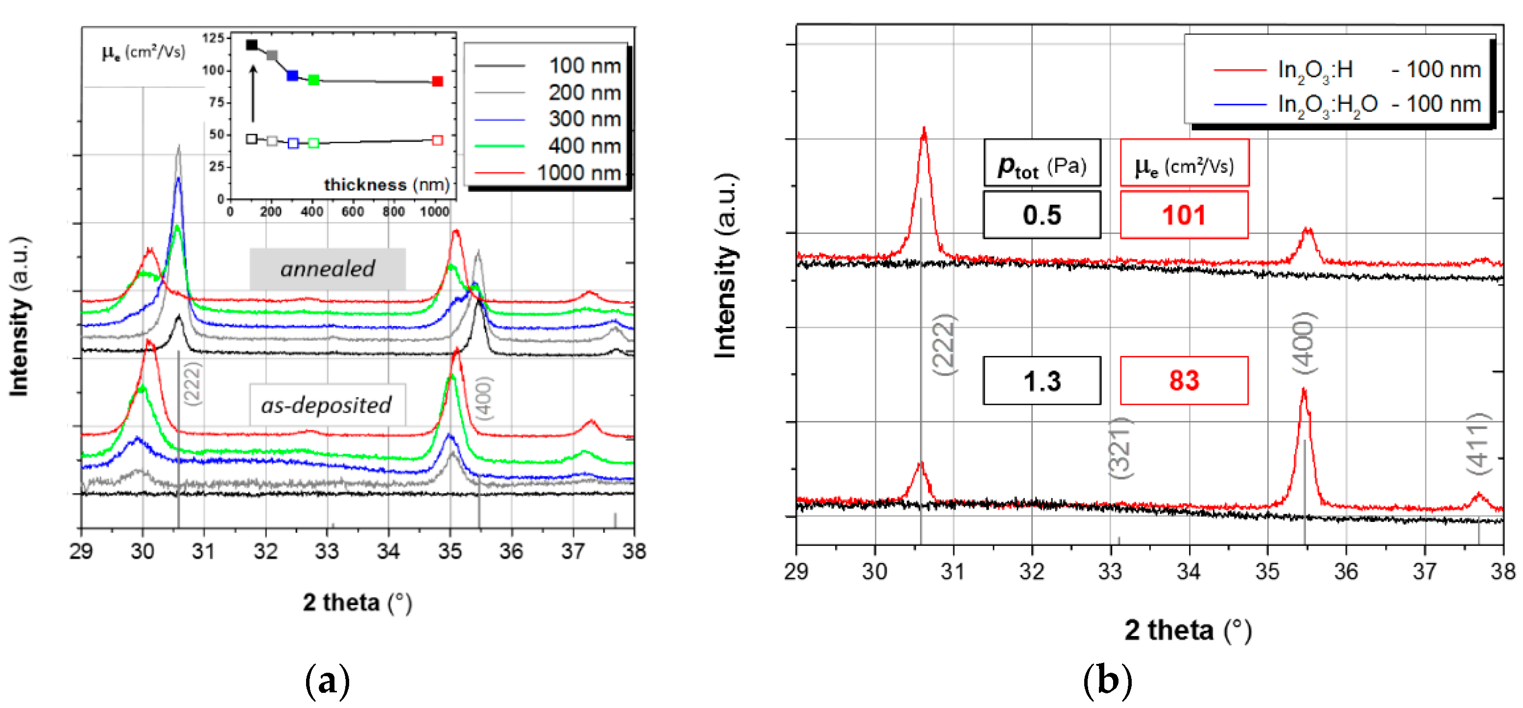
3.1. Crystallinity versus Electron Mobility
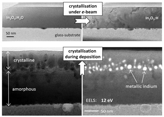
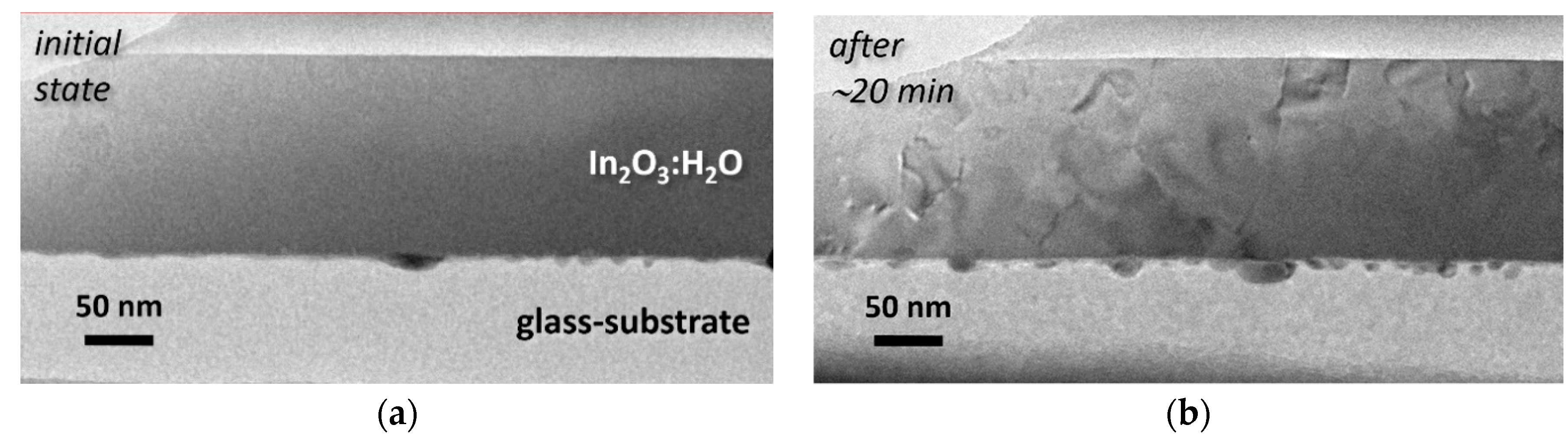
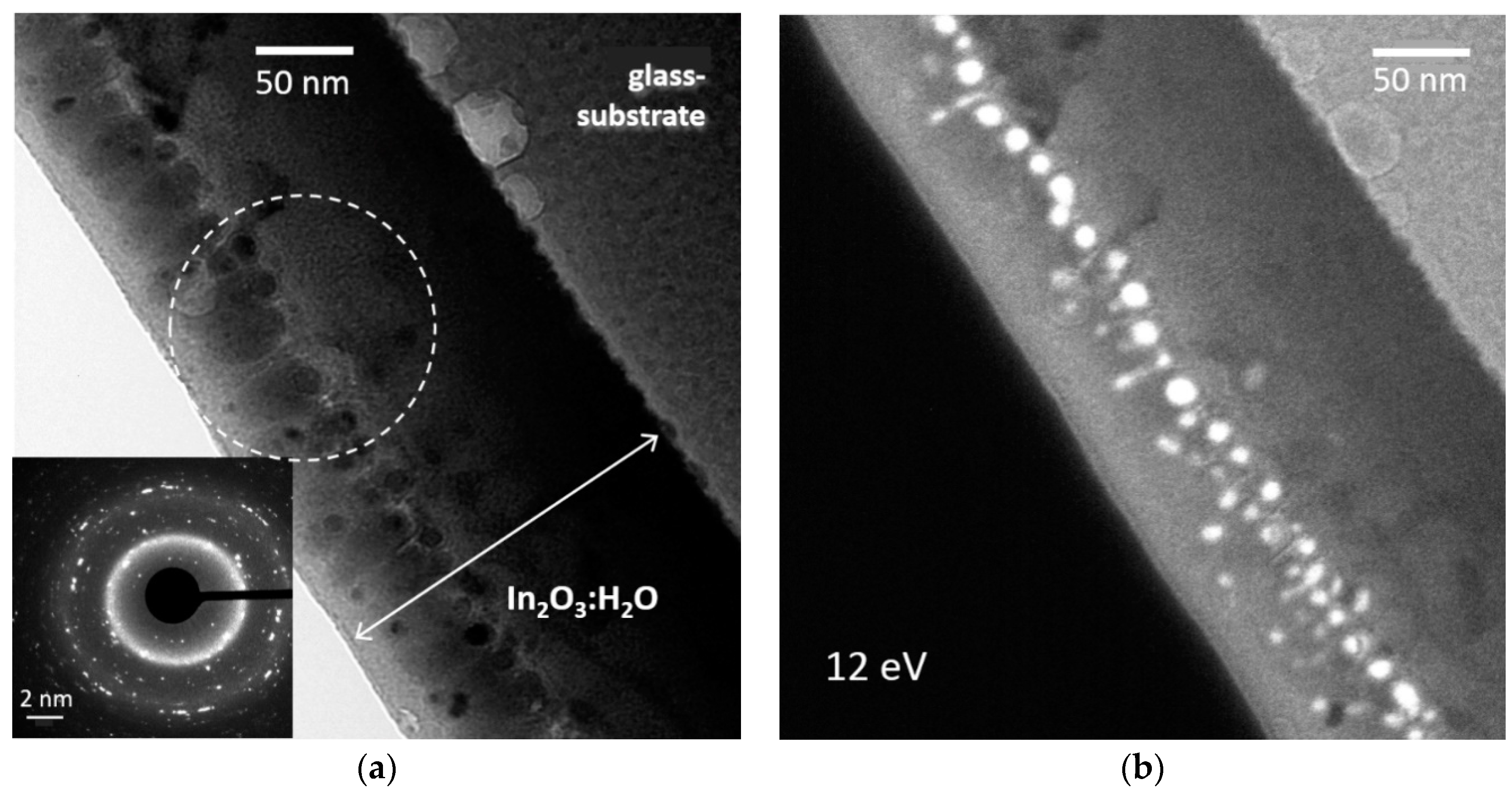
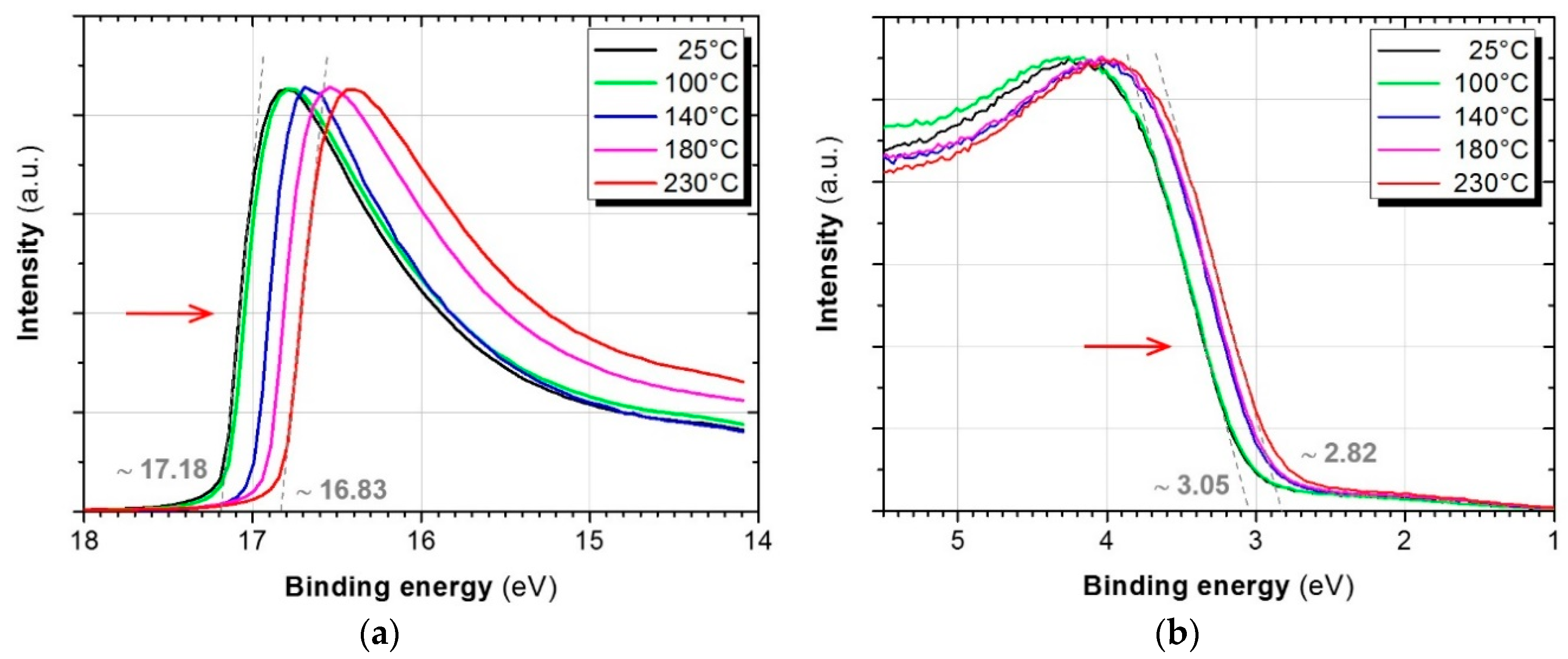
3.2. Presence and Role of Metallic Indium
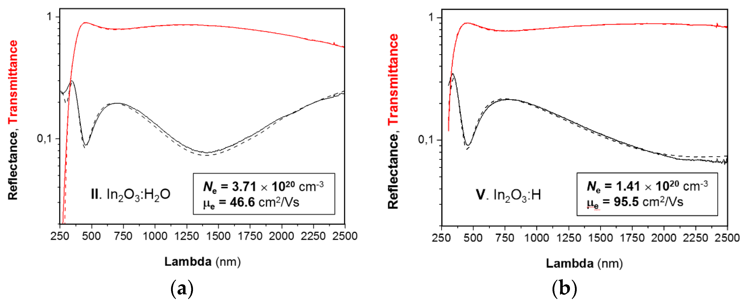
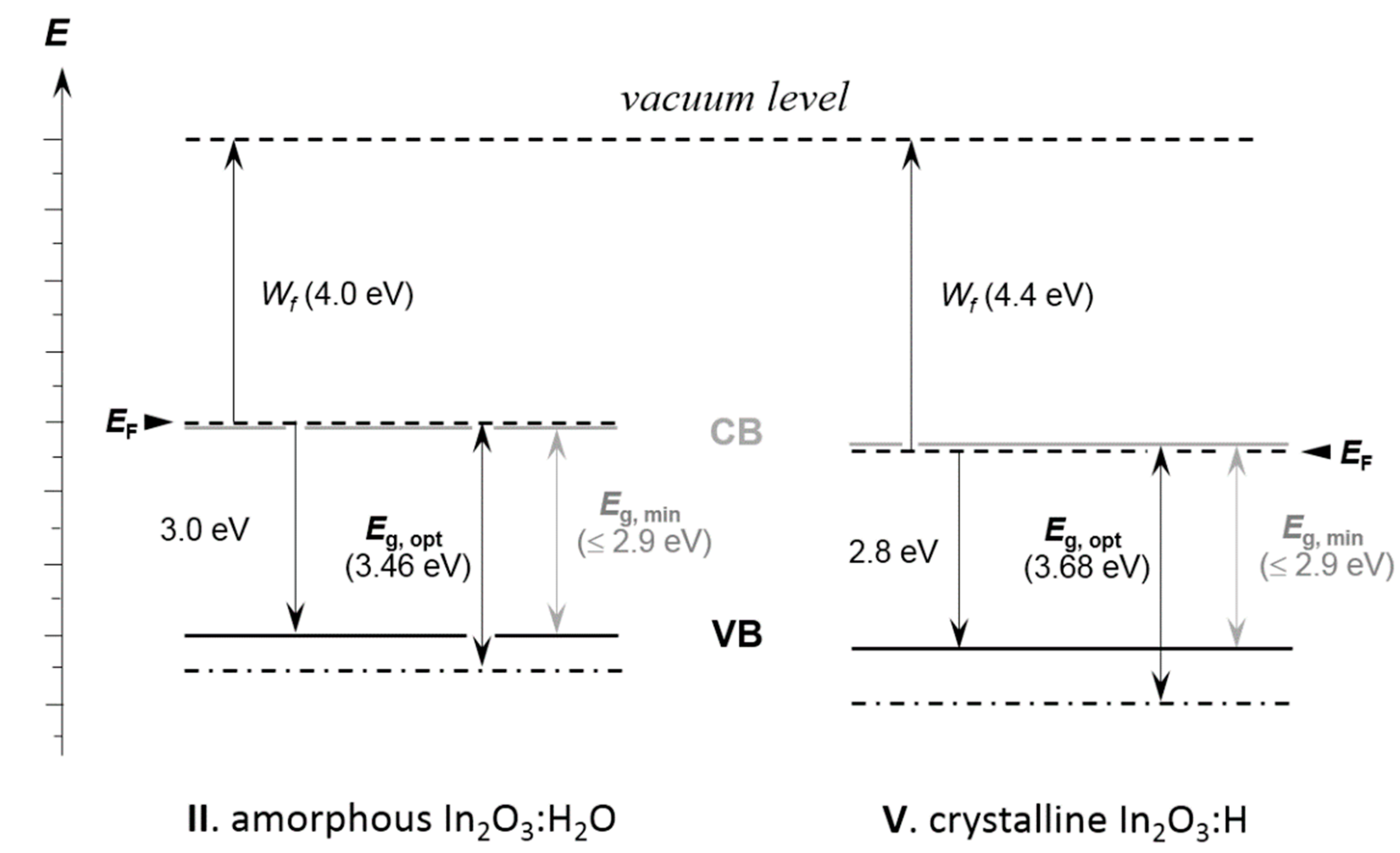
3.3. Optical Properties of In2O3:H2O and In2O3:H
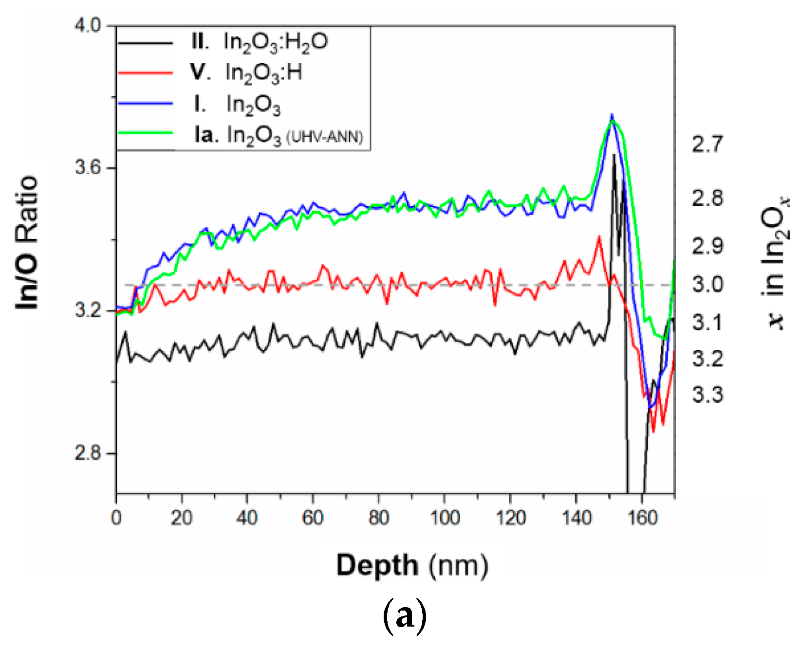
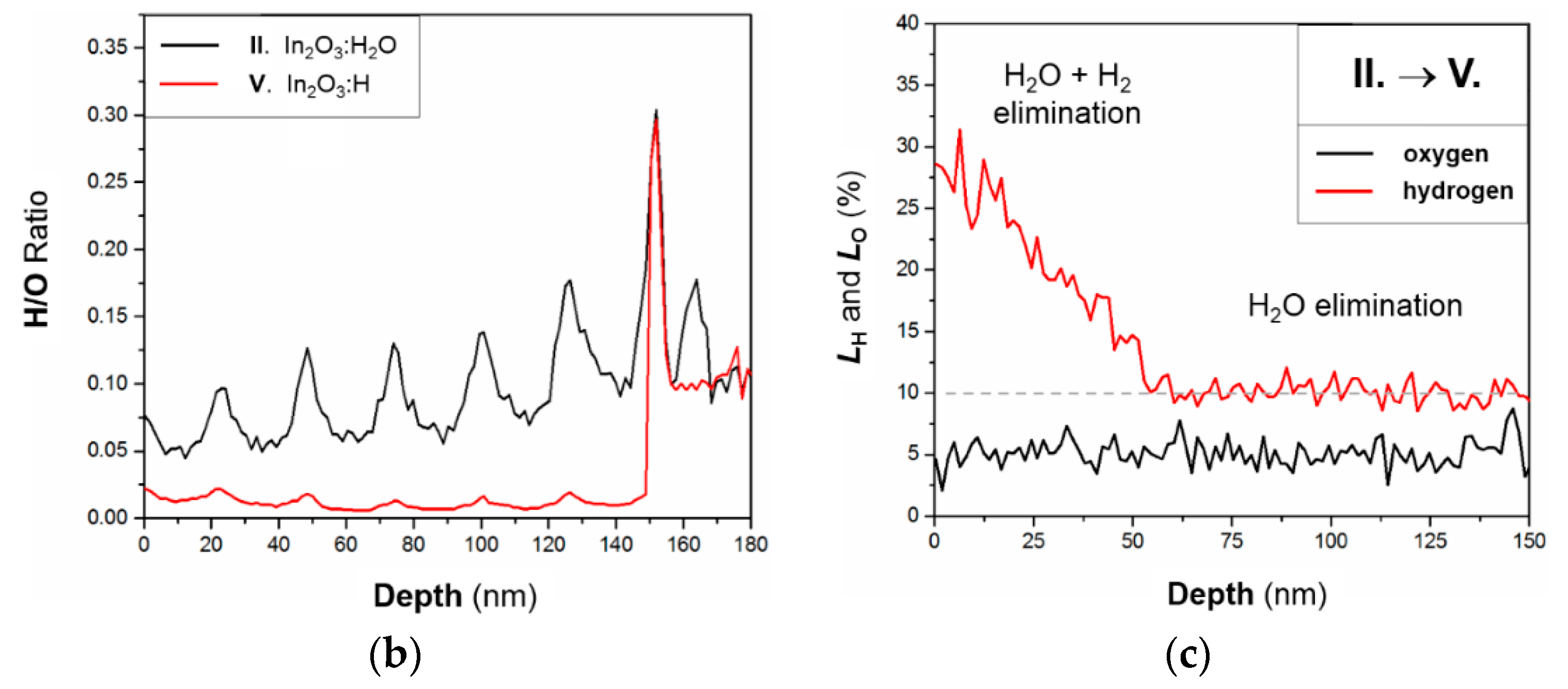
3.4. Chemical Changes in In2O3
4. Discussion
4.1. Appearance of Metallic Indium in In2O3
4.2. Water Containing In2O3
4.3. Doping and Conductivity of In2O3
4.4. High-Mobility of In2O3:H
5. Conclusions
Supplementary Materials
Author Contributions
Funding
Acknowledgments
Conflicts of Interest
References
- Koida, T.; Fujiwara, H.; Kondo, M. Hydrogen-doped In2O3 as High-mobility Transparent Conductive Oxide. Jpn. J. Appl. Phys. 2007, 46, L685–L687. [Google Scholar] [CrossRef]
- Koida, T.; Fujiwara, H.; Kondo, M. Structural and electrical properties of hydrogen-doped In2O3 films fabricated by solid-phase crystallization. J. Non-Cryst. Solids 2008, 354, 2805–2808. [Google Scholar] [CrossRef]
- Scherg-Kurmes, H.; Koerner, S.; Ring, S.; Klaus, M.; Korte, L.; Ruske, F.; Schlatmann, R.; Rech, B.; Szyszka, B. High mobility In2O3:H as contact layer for a-Si:H/c-Si heterojunction and mc-Si:H thin film solar cells. Thin Solid Films 2015, 594, 316–322. [Google Scholar] [CrossRef]
- Koida, T.; Fujiwara, H.; Kondo, M. High-mobility hydrogen-doped transparent conductive oxide for a-Si:H/c-Si heterojunction solar cells. Sol. Energy Mater. Sol. Cells 2009, 93, 851–854. [Google Scholar] [CrossRef]
- Battaglia, C.; Erni, L.; Boccard, M.; Barraud, L.; Escarre, J.; Soderstrom, K.; Bugnon, G.; Billet, A.; Ding, L.; Despeisse, M.; et al. Micromorph thin-film silicon solar cells with transparent high-mobility hydrogenated indium oxide front electrodes. J. Appl. Phys. 2011, 109, 114501. [Google Scholar] [CrossRef]
- Jäger, T.; Romanyuk, Y.E.; Bissig, B.; Pianezzi, F.; Nishiwaki, S.; Reinhard, P.; Steinhauser, J.; Schwenk, J.; Tiwari, A.N. Improved open-circuit voltage in Cu(In,Ga)Se2 solar cells with high work function transparent electrodes. J. Appl. Phys. 2015, 117, 225303. [Google Scholar]
- Jäger, T.; Romanyuk, Y.E.; Nishiwaki, S.; Bissig, B.; Pianezzi, F.; Fuchs, P.; Gretener, C.; Döbeli, M.; Tiwari, A.N. Hydrogenated indium oxide window layers for high-efficiency Cu(In,Ga)Se2 solar cells. J. Appl. Phys. 2015, 117, 205301. [Google Scholar] [CrossRef]
- Keller, J.; Aijaz, A.; Gustavsson, F.; Kubart, T.; Stolt, L.; Edoff, M.; Törndahl, T. Direct comparison of atomic layer deposition and sputtering of In2O3:H used as transparent conductive oxide layer in CuIn1−xGaxSe2 thin film solar cells. Sol. Energy Mater. Sol. Cells 2016, 157, 757–764. [Google Scholar] [CrossRef]
- Wardenga, H.F.; Frischbier, M.V.; Morales-Masis, M.; Klein, A. In Situ Hall Effect Monitoring of Vacuum Annealing of In2O3:H Thin Films. Materials 2015, 8, 561–574. [Google Scholar] [CrossRef]
- Bielz, T.; Lorenz, H.; Jochum, W.; Kaindl, R.; Klauser, F.; Klötzer, B.; Penner, S. Hydrogen on In2O3: Reducibility, Bonding, Defect Formation, and Reactivity. J. Phys. Chem. C 2010, 114, 9022–9029. [Google Scholar] [CrossRef]
- Steigert, A.; Lauermann, I.; Niesen, T.; Dalibor, T.; Palm, J.; Körner, S.; Scherg-Kurmes, H.; Muydinov, R.; Szyszka, B.; Klenk, R. Sputtered Zn(O,S)/In2O3:H window layers for enhanced blue response of chalcopyrite solar cells. Phys. Status Solidi RRL 2015, 9, 627–630. [Google Scholar] [CrossRef]
- Dewald, W.; Sittinger, V.; Werner, W.; Jacobs, C.; Szyszka, B. Optimization of process parameters for sputtering of ceramic ZnO:Al2O3 targets for a-Si:H/µc-Si:H solar cells. Thin Solid Films 2009, 518, 1085–1090. [Google Scholar] [CrossRef]
- Scherg-Kurmes, H.; Hafez, A.; Siemers, M.; Pflug, A.; Schlatmann, R.; Rech, B.; Szyszka, B. Improvement of the homogeneity of high mobility In2O3:H films by sputtering through a mesh electrode studied by Monte Carlo simulation and thin film analysis. Phys. Status Solidi A 2016, 213, 2310–2316. [Google Scholar] [CrossRef]
- Lauermann, I.; Steigert, A. CISSY: A station for preparation and surface/ interface analysis of thin film materials and devices. J. Large-Scale Res. Fac. 2016, 2, A67. [Google Scholar] [CrossRef]
- Storms, H.; Brown, K.; Stein, J. Evaluation of a cesium positive ion source for secondary ion mass spectrometry. Anal. Chem. 1977, 49, 2023–2030. [Google Scholar] [CrossRef]
- Gao, Y. A new secondary ion mass spectrometry technique for III-V semiconductor compounds using the molecular ions CsM+. J. Appl. Phys. 1988, 64, 3760–3762. [Google Scholar] [CrossRef]
- Magee, C.; Harrington, W.; Botnick, E. On the use of CsX+ cluster ions for major element depth profiling in secondary ion mass spectrometry. Int. J. Mass. Spectrom. Ion Process. 1990, 103, 45–56. [Google Scholar] [CrossRef]
- Mikami, A. Investigation of SiCs+, GeCs+ and SiCs2+ Secondary Ion Emission from Si1−xGex. Jpn. J. Appl. Phys. 2004, 43, 2745. [Google Scholar] [CrossRef]
- Saha, B.; Chakraborty, P. MCsn+-SIMS: An Innovative Approach for Direct Compositional Analysis of Materials without Standards. Energy Procedia 2013, 41, 80–109. [Google Scholar] [CrossRef]
- Odaka, H.; Iwata, S.; Taga, N.; Ohnishi, S.; Kaneta, Y.; Shigesato, Y. Study on electronic structure and optoelectronic properties of indium oxide by first-principles calculation. Jpn. J. App. Phys. 1997, 36, 5551–5554. [Google Scholar] [CrossRef]
- Mryasov, O.N.; Freeman, A.J. Electronic band structure of indium tin oxide and criteria for transparent conducting behaviour. Phys. Rev. B 2001, 64, 233111. [Google Scholar] [CrossRef]
- Robertson, J.; Falabretti, B. Handbook of Transparent Conductors; Ginley, D.S., Ed.; Springer Science + Business Media, LLC: Berlin/Heidelberg, Germany, 2010. [Google Scholar] [CrossRef]
- Preissler, N.; Bierwagen, O.; Ramu, A.T.; Speck, J.S. Electrical transport, electrothermal transport, and effective electron mass in single-crystalline In2O3 films. Phys. Rev. B 2013, 88, 085305. [Google Scholar] [CrossRef]
- Galazka, Z.; Uecker, R.; Irmscher, K.; Schulz, D.; Klimm, D.; Albrecht, M.; Pietsch, M.; Ganschow, S.; Kwasniewski, A.; Fornari, R. Melt growth, characterization and properties of bulk In2O3 single crystals. J. Cryst. Growth 2013, 362, 349–352. [Google Scholar] [CrossRef]
- Minami, T.; Kuboi, T.; Miyata, T.; Ohtani, Y. Stability in a high humidity environment of TCO thin films deposited at low temperatures. Phys. Status Solidi A 2008, 205, 255–260. [Google Scholar] [CrossRef]
- Ellmer, K.; Mientus, R. Carrier transport in polycrystalline ITO and ZnO:Al II: The influence of grain barriers and boundaries. Thin Solid Films 2008, 516, 5829–5835. [Google Scholar] [CrossRef]
- Kima, H.-K.; Lee, K.-S. Effect of Introducing H2O Vapor on Properties of RF Sputter-Grown ITO Anode Layer for OLEDs. Electrochem. Solid-State Lett. 2008, 11, J57–J59. [Google Scholar] [CrossRef]
- Krishnasamy, J.; Chan, K.-Y.; Tou, T.-Y. Influence of process parameters on the substrate heating in direct current plasma magnetron sputtering deposition process. Microelectron. Int. 2010, 27, 75–78. [Google Scholar] [CrossRef]
- Buchholz, D.B.; Ma, Q.; Alducin, D.; Ponce, A.; Jose-Yacaman, M.; Khanal, R.; Medvedeva, J.E.; Chang, R.P.H. The Structure and Properties of Amorphous Indium Oxide. Chem. Mater. 2014, 26, 5401–5411. [Google Scholar] [CrossRef]
- Scherrer, P. Bestimmung der Größe und der inneren Struktur von Kolloidteilchen mittels Röntgenstrahlen. Göttinger Nachr. Gesell. 1918, 2, 98–100. [Google Scholar]
- Genzel, C. X-ray residual stress analysis in thin films under grazing incidence—Basic aspects and applications. Mater. Sci. Technol. 2005, 21, 10–18. [Google Scholar] [CrossRef]
- Bartolomé, J.; Hidalgo, P.; Maestre, D.; Cremades, A.; Piqueras, J. In-Situ Scanning Electron Microscopy and Atomic Force Microscopy Young’s Modulus Determination of Indium Oxide Microrods for Micromechanical Resonator Applications. Appl. Phys. Lett. 2014, 104, 161909. [Google Scholar] [CrossRef]
- Zhang, K.H.L.; Regoutz, A.; Palgrave, R.G.; Payne, D.J.; Egdell, R.G. Determination of the Poisson ratio of (001) and (111) oriented thin films of In2O3 by synchrotron-based X-ray diffraction. Phys. Rev. B 2011, 84, 233301. [Google Scholar] [CrossRef]
- Remy, H. Treatise on Inorganic Chemistry: Volume 1; Elsevier: Amsterdam, The Netherlands, 1956; ISBN 978-0444404701. [Google Scholar]
- Egerton, R.F.; Li, P.; Malac, M. Radiation damage in the TEM and SEM. Micron 2004, 35, 399–409. [Google Scholar] [CrossRef] [PubMed]
- Joseph, S.; Berger, S. A study of crystallographic phases in non-stoichiometric (oxygen deficiency) indium oxide thin films. J. Mater. Sci. 2017, 52, 1988–1995. [Google Scholar] [CrossRef]
- Guenther, G.; Schierning, G.; Theissmann, R.; Kruk, R.; Schmechel, R.; Baehtz, C.; Prodi-Schwab, A. Formation of metallic indium-tin phase from indium-tin-oxide nanoparticles under reducing conditions and its influence on the electrical properties. J. Appl. Phys. 2008, 104, 034501. [Google Scholar] [CrossRef]
- Okamoto, H. In-O (Indium-Oxygen). JPEDAV 2007, 28, 591–592. [Google Scholar] [CrossRef]
- Aiyama, T.; Yada, T.J. Plasmon damping in In, Cd and graphite. J. Phys. Soc. Jpn. 1975, 38, 1357–1361. [Google Scholar] [CrossRef]
- Boulenouar, K.; Bouslama, M.; Mokadem, A.; Vizzini, S.; Lounis, Z.; Abdellaoui, A.; Reguad, B.; Bedrouni, M.; Hamaida, K.; Guenouna, T.; et al. Auger Electron Spectroscopy, Electron Energy Loss Spectroscopy, UV Photoelectron Spectroscopy, and Photoluminescence Characterization of In2O3 Associated to the Theoretical Calculations Based on the Generalized Gradient Approximation and Modified Becke Johnson. J. Phys. Chem. C 2017, 121, 8345–8352. [Google Scholar]
- Scheel, H.J. Crystal Growth Technology; Scheel, H.J., Fukuda, T., Eds.; John Wiley & Sons, Ltd.: Chichester, UK, 2003; 694p, ISBN 0-471-49059-8. [Google Scholar]
- Namkoong, G.; Trybus, E.; Lee, K.K.; Moseley, M.; Doolittle, W.A.; Look, D.C. Metal modulation epitaxy growth for extremely high hole concentrations above 1019 cm−3 in GaN. Appl. Phys. Lett. 2008, 93, 172112. [Google Scholar] [CrossRef]
- Molodyk, A.A.; Korsakov, I.E.; Novojilov, M.A.; Graboy, I.E.; Kaul, A.R.; Wahl, G. Volatile Surfactant-Assisted MOCVD: Application to LaAlO3 Thin-Film Growth. Chem. Vapor Depos. 2000, 6, 133–138. [Google Scholar] [CrossRef]
- Koida, T.; Kondo, M.; Tsutsumi, K.; Sakaguchi, A.; Suzuki, M.; Fujiwara, H. Hydrogen-Doped In2O3 Transparent Conducting Oxide Films Prepared By Solid-Phase Crystallization Method. J. Appl. Phys. 2010, 107, 033514. [Google Scholar] [CrossRef]
- Macco, B.; Knoops, H.C.M.; Kessels, W.M.M. Electron Scattering and Doping Mechanisms in Solid-PhaseCrystallized In2O3:H Prepared by Atomic Layer Deposition. ACS Appl. Mater. Interfaces 2015, 7, 16723–16729. [Google Scholar] [CrossRef] [PubMed]
- Muranaka, S.; Bando, Y.; Takada, T. Influence of substrate temperature and film thickness on the structure of reactively evaporated In2O3 films. Thin Solid Films 1987, 151, 355–364. [Google Scholar] [CrossRef]
- Pflug, A.; Sittinger, V.; Ruske, F.; Szyszka, B.; Dittmar, G. Optical characterization of aluminum-doped zinc oxide films by advanced dispersion theories. Thin Solid Films 2004, 455–456, 201–206. [Google Scholar] [CrossRef]
- Wirtz, G.P.; Takiar, H.P. Oxygen Diffusion in Vapor-Deposited Indium Oxide Films. J. Am. Ceram. Soc. 1981, 64/12, 748–752. [Google Scholar] [CrossRef]
- Pan, C.A.; Ma, T.P. Work function of In2O3 film as determined from internal photoemission. Appl. Phys. Lett. 1980, 37, 714–716. [Google Scholar] [CrossRef]
- Hohmann, M.V.; Ágoston, P.; Wachau, A.; Bayer, T.J.; Brötz, J.; Albe, K.; Klein, A. Orientation dependent ionization potential of In2O3: A natural source for inhomogeneous barrier formation at electrode interfaces in organic electronics. J. Phys. Condens. Matter 2011, 23, 334203. [Google Scholar] [CrossRef]
- Shaker, A.; Zekry, A. A New and Simple Model for Plasma-and Doping-Induced Band Gap Narrowing. J. Electron Devices 2010, 8, 293–299. [Google Scholar]
- Jia, J.; Oka, N.; Shigesato, Y. Direct observation of the band gap shrinkage in amorphous In2O3–ZnO thin films. J. Appl. Phys. 2013, 113, 163702. [Google Scholar] [CrossRef]
- Vanýsek, P. Handbook of Chemistry and Physics, 81th ed.; Electrochemical Series; CRC Press LLC: Boca Raton, FL, USA, 2000; ISBN 978-0849304811. [Google Scholar]
- Schoeller, H.E. Thermodynamics and Kinetics of Oxidation and Temperature Dependent Mechanical Characterization of Pure Indium Solder. Ph.D. Thesis, State University of New York, Binghamton, NY, USA, 2007. UMI Number: 1447566. [Google Scholar]
- Mukhopadhyay, S.; Gowtham, S.; Pandey, R.; Costales, A. Theoretical study of small clusters of indium oxide: InO, In2O, InO2, In2O2. J. Mol. Struct. THEOCHEM 2010, 948, 31–35. [Google Scholar] [CrossRef]
- Gordon, D.F.; Helle, M.H.; Jones, T.G.; Fung, K. CHMWTR: A Plasma Chemistry Code for Water Vapor; NRL/MR/6790-12-9383; Naval Research Laboratory Report: Washington, WA, USA, 2011. [Google Scholar]
- Coburn, J.W.; Taglauer, E.; Kay, E. A study of the neutral species rf-sputtered from oxide targets. Jpn. J. Appl. Phys. Suppl. 1974, 2, 501–504. [Google Scholar] [CrossRef]
- Snyder, D.; Carmichael, I.S.E. Olivine-liquid equilibria and the chemical activities of FeO, NiO, Fe2O3, and MgO in natural basic melts. Geochim. Cosmochim. Acta 1991, 56, 303–318. [Google Scholar] [CrossRef]
- Chatterji, D.; Vest, R.W. Thermodynamic Properties of the System Indium-Oxygen. J. Am. Ceram. Soc. 1972, 55, 575–578. [Google Scholar] [CrossRef]
- Coburn, J.W.; Kay, E. Positive-ion bombardment of substrates in rf diode glow discharge sputtering. J. Appl. Phys. 1972, 43, 4965–4971. [Google Scholar] [CrossRef]
- Tominaga, K.; Sueyoshi, Y.; Munfei, Ch.; Chintani, Y. Energetic O- ions and O atoms in planar magnetron sputtering of ZnO target. Jpn. J. Appl. Phys. 1993, 32, 4131–4135. [Google Scholar] [CrossRef]
- Pierre, A.C. Gelation of Aluminum Hydroxide Sols. J. Am. Ceram. Soc. 1987, 70, 28–32. [Google Scholar] [CrossRef]
- Koga, N.; Kimizu, T. Thermal Decomposition of Indium (III) Hydroxide Prepared by the Microwave-Assisted Hydrothermal Method. J. Am. Ceram. Soc. 2008, 91, 4052–4058. [Google Scholar] [CrossRef]
- Jost, G.C.E.; Hamri, A.N.; Köhler, F.; Hüpkes, J. Reliability aspects of hydrogen-doped indium oxide. Phys. Status Solidi A 2016, 213, 1751–1759. [Google Scholar] [CrossRef]
- Sudakar, C.; Dixit, A.; Kumar, S.; Sahana, M.B.; Lawes, G.; Naika, R.; Naik, V.M. Coexistence of anion and cation vacancy defects in vacuum-annealed In2O3 thin films. Scr. Mater. 2010, 62, 63–66. [Google Scholar] [CrossRef]
- King, P.D.C.; Lichti, R.L.; Celebi, Y.G.; Gil, J.M.; Vilão, R.C.; Alberto, H.V.; Duarte, J.P.; Payne, D.J.; Egdell, R.G.; McKenzie, I.; et al. Shallow donor state of hydrogen in In2O3 and SnO2: Implications for conductivity in transparent conducting oxides. Phys. Rev. B 2009, 80, 081201(R). [Google Scholar] [CrossRef]
- Agoston, P.; Albe, K.; Nieminen, R.M.; Puska, M.J. Intrinsic n-type behavior in transparent conducting oxides: A comparative hybrid-functional study of In2O3, SnO2, and ZnO. Phys. Rev. Lett. 2009, 103, 245501. [Google Scholar] [CrossRef] [PubMed]
- De Wit, J.H.W. Structural Aspects and Defect Chemistry in In2O3. J. Sol. St. Chem. 1977, 20, 143–148. [Google Scholar] [CrossRef]
- Liu, J.; Liu, T.; Liu, F.; Li, H. Thermodynamics of native defects in In2O3 crystals using a first-principles method. RSC Adv. 2014, 4, 36983–36989. [Google Scholar] [CrossRef]
- Reunchan, P.; Zhou, X.; Limpijumnong, S.; Janotti, A.; Van de Walle, C.G. Vacancy defects in indium oxide: An ab-initio study. Curr. Appl. Phys. 2011, 11, S296–S300. [Google Scholar] [CrossRef]
- Limpijumnong, S.; Reunchan, P.; Janotti, A.; Van de Walle, C.G. Hydrogen doping in indium oxide: An ab initio study. Phys. Rev. B 2009, 80, 193202. [Google Scholar] [CrossRef]
- Tomita, T.; Yamashita, K.; Hayafuji, Y. The origin of n-type conductivity in un-doped In2O3. Appl. Phys. Lett. 2005, 87, 051911. [Google Scholar] [CrossRef]
- Shannon, R.D. Revised Effective Ionic Radii and Systematic Studies of Interatomie Distances in Halides and Chaleogenides. Acta Cryst. A 1976, 32, 751–767. [Google Scholar] [CrossRef]
- Bushema, I.S.; Headridge, J.B. Determination of indium by hydride generation and atomic-absorption spectrometry. Talanta 1982, 29, 519–520. [Google Scholar] [CrossRef]
- Raghavachari, K.; Fu, Q.; Chen, G.; Li, L.; Li, C.H.; Law, D.C.; Hicks, R.F. Hydrogen Adsorption on the Indium-Rich Indium Phosphide (001) Surface: A Novel Way to Produce Bridging In-H-In Bonds. J. Am. Chem. Soc. 2002, 124, 15119–15124. [Google Scholar] [CrossRef]
- Lany, S.; Zunger, A. Comment on “Intrinsic n-type Behavior in Transparent Conducting Oxides: A Comparative Hybrid-Functional Study of In2O3, SnO2, and ZnO”. Phys. Rev. Lett. 2011, 106, 069601. [Google Scholar] [CrossRef]
- Ohya, Y.; Yamamoto, T.; Ban, T. Equilibrium Dependence of the Conductivity of Pure and Tin-Doped Indium Oxide on Oxygen Partial Pressure and Formation of an Intrinsic Defect Cluster. J. Am. Ceram. Soc. 2008, 91, 240–245. [Google Scholar] [CrossRef]
- Szczyrbowski, J.; Dietrich, A.; Hoffmann, H. Optical Properties of RF-Sputtered Indium Oxide Films. Phys. Stat. Sol. A 1982, 69, 217–226. [Google Scholar] [CrossRef]
- Ibragimov, Kh.I.; Korol’kov, V.A. Temperature Dependence of the Work Function of Metals and Binary Alloys. Inorg. Mater. 2001, 37, 567–572. [Google Scholar] [CrossRef]
- Claflin, B.; Fritzsche, H. The Role of Oxygen Diffusion in Photoinduced Changes of the Electronic and Optical Properties in Amorphous Indium Oxide. J. Electron. Mater. 1996, 25, 1772–1777. [Google Scholar] [CrossRef]
- Guilmeau, E.; Berardan, D.; Simon, C.; Maignan, A.; Raveau, B.; Ovono, D.O.; Delorme, F. Tuning the transport and thermoelectric properties of In2O3 bulk ceramics through doping at In-site. J. Appl. Phys. 2009, 106, 053715. [Google Scholar] [CrossRef]


| States | I. In2O3 As-Deposited w/o Heating | II. In2O3:H2O As-Deposited w/o Heating | III. In2O3:H2O As-Deposited Tdep = 160 °C | IV. In2O3:H Tann = 180 °C, Ambient Air | V. In2O3:H Tann = 230 °C, UHV |
|---|---|---|---|---|---|
| Dlong (nm) | 35 ± 6 | - | 50 ± 15 | 165 ± 6 | 328 ± 5 * |
| Dlat (nm) | 22 ± 2 | - | 32 ± 2 | 230 ± 60 | 205 ± 20 |
| Residual Stress (GPa) | −2.1 ± 0.8 | - | −1.9 ± 0.6 | −0.5 ± 0.1 | −0.6 ± 0.2 |
| μe (cm2/V⋅s) | 22 | 47 | 41 | 117 | 118 |
| Ne (cm−3) | 4.58 × 10²⁰ | 5.85 × 10²⁰ | 2.03 × 10²⁰ | 2.24 × 10²⁰ | 2.57 × 10²⁰ |
| States → Band Gap/Thickness ↓ | I. In2O3 As-Deposited w/o Heating | II. In2O3:H2O As-Deposited w/o Heating | V. In2O3:H Tann = 230 °C, UHV |
|---|---|---|---|
| Eg (eV)/100 nm 400 nm | 3.55 3.50 | 3.46 3.48 | 3.68 3.65 |
© 2019 by the authors. Licensee MDPI, Basel, Switzerland. This article is an open access article distributed under the terms and conditions of the Creative Commons Attribution (CC BY) license (http://creativecommons.org/licenses/by/4.0/).
Share and Cite
Muydinov, R.; Steigert, A.; Wollgarten, M.; Michałowski, P.P.; Bloeck, U.; Pflug, A.; Erfurt, D.; Klenk, R.; Körner, S.; Lauermann, I.; et al. Crystallisation Phenomena of In2O3:H Films. Materials 2019, 12, 266. https://doi.org/10.3390/ma12020266
Muydinov R, Steigert A, Wollgarten M, Michałowski PP, Bloeck U, Pflug A, Erfurt D, Klenk R, Körner S, Lauermann I, et al. Crystallisation Phenomena of In2O3:H Films. Materials. 2019; 12(2):266. https://doi.org/10.3390/ma12020266
Chicago/Turabian StyleMuydinov, Ruslan, Alexander Steigert, Markus Wollgarten, Paweł Piotr Michałowski, Ulrike Bloeck, Andreas Pflug, Darja Erfurt, Reiner Klenk, Stefan Körner, Iver Lauermann, and et al. 2019. "Crystallisation Phenomena of In2O3:H Films" Materials 12, no. 2: 266. https://doi.org/10.3390/ma12020266
APA StyleMuydinov, R., Steigert, A., Wollgarten, M., Michałowski, P. P., Bloeck, U., Pflug, A., Erfurt, D., Klenk, R., Körner, S., Lauermann, I., & Szyszka, B. (2019). Crystallisation Phenomena of In2O3:H Films. Materials, 12(2), 266. https://doi.org/10.3390/ma12020266