Nanotribological Properties of Ga- and N-Faced Bulk Gallium Nitride Surfaces Determined by Nanoscratch Experiments

Abstract
1. Introduction
2. Materials and Methods
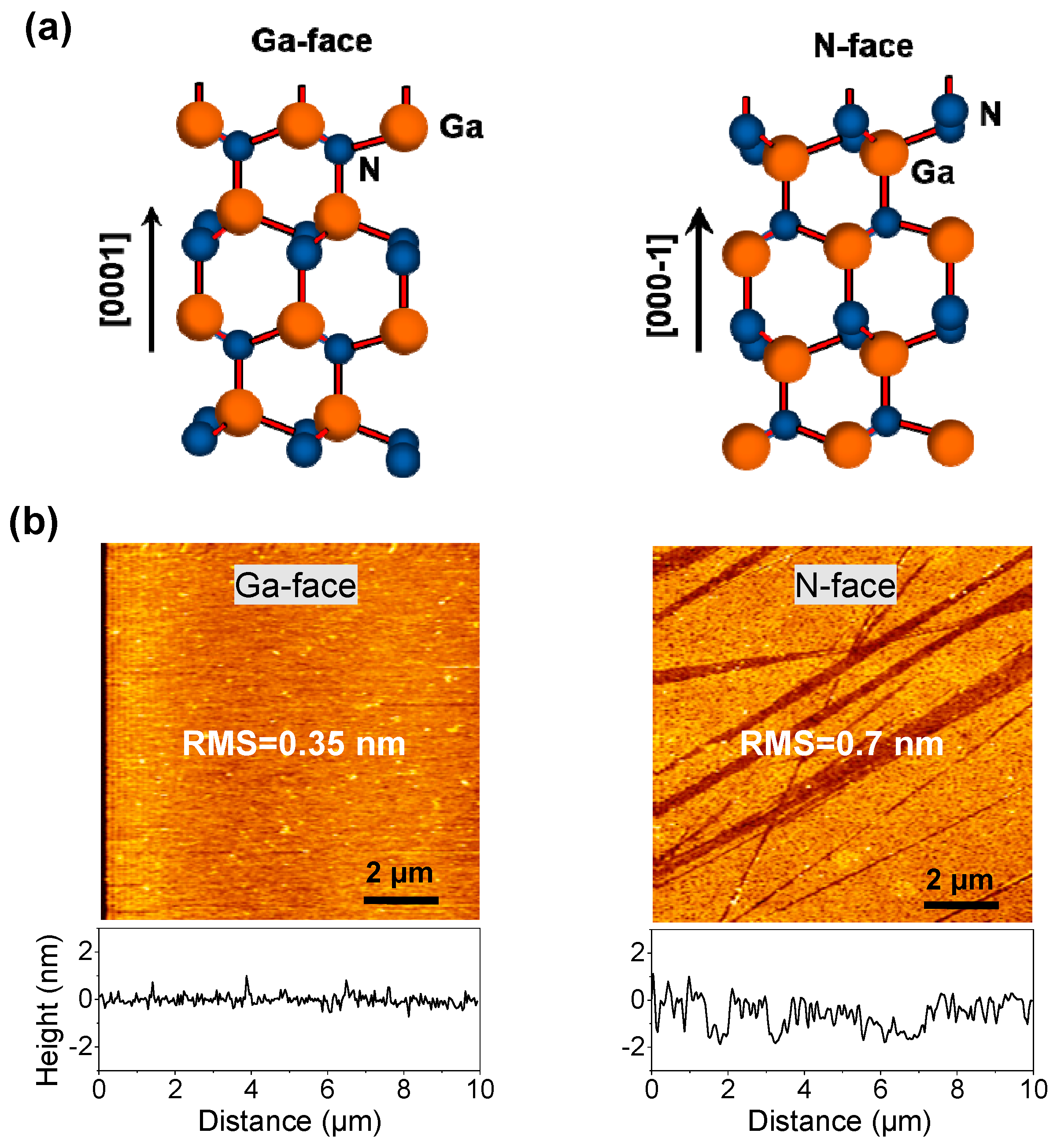
2.1. GaN Material
2.2. Nanoindentation and Nanoscratch Experiments
2.3. HRTEM and XPS Characterization
3. Results and Discussion
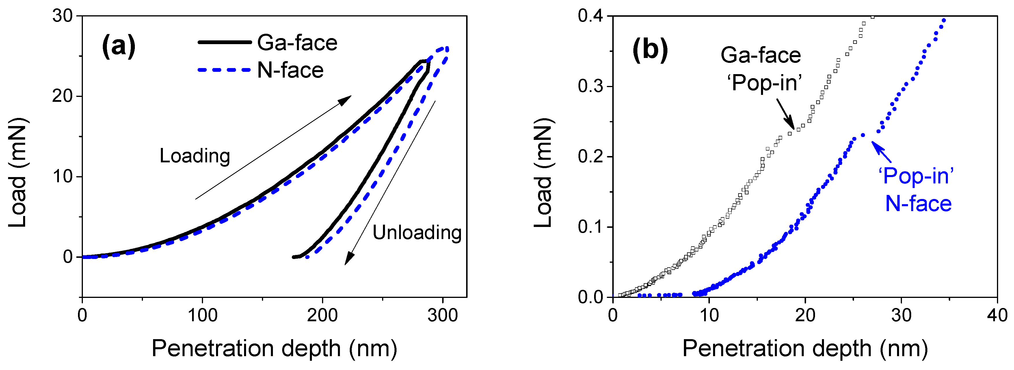
3.1. Nanoindentation Tests on Ga- and N-Faced GaN Samples
3.2. Nanotribological Properties on Ga- and N-Faced GaN Samples
3.3. Explanation of the Difference in Nanotribological Properties for Ga- and N-Faced GaN Samples
4. Conclusions
Author Contributions
Funding
Acknowledgments
Conflicts of Interest
References
- Pust, P.; Schmidt, P.J.; Schnick, W. A revolution in lighting. Nat. Mater. 2015, 14, 454. [Google Scholar] [CrossRef] [PubMed]
- Tsao, J.Y.; Crawford, M.H.; Coltrin, M.E.; Fischer, A.J.; Koleske, D.D.; Subramania, G.S.; Wang, G.T.; Wierer, J.J.; Karlicek, R.F., Jr. Toward smart and ultra-efficient solid-state lighting. Adv. Opt. Mater. 2014, 2, 809–836. [Google Scholar] [CrossRef]
- Roccaforte, F.; Greco, G.; Fiorenza, P.; Iucolano, F. An overview of normally-off GaN-based high electron mobility transistors. Materials 2019, 12, 1599. [Google Scholar] [CrossRef] [PubMed]
- Zeng, F.; An, J.X.; Zhou, G.; Li, W.; Wang, H.; Duan, T.; Jiang, L.; Yu, H. A comprehensive review of recent progress on GaN high electron mobility transistors: devices, fabrication and reliability. Electronics 2018, 7, 377. [Google Scholar] [CrossRef]
- Mishra, U.K.; Shen, L.; Kazior, T.E.; Wu, Y. GaN-based RF power devices and amplifiers. Proc. IEEE 2008, 96, 287–305. [Google Scholar] [CrossRef]
- Meneghesso, G.; Meneghini, M.; Zanoni, E. Gallium Nitride-Enabled High Frequency and High Efficiency Power Conversion; Springer: New York, NY, USA, 2018. [Google Scholar]
- Fang, T.-H.; Chang, W.-J.; Lin, C.-M. Nanoindentation and nanoscratch characteristics of Si and GaAs. Microelectron. Eng. 2005, 77, 389–398. [Google Scholar] [CrossRef]
- Fang, T.-H.; Chang, W.-J.; Lin, C.-M. Nanoindentation characterization of ZnO thin films. Mat. Sci. Eng. A 2007, 452–453, 715–720. [Google Scholar] [CrossRef]
- Jain, S.C.; Willander, M.; Narayan, J.; Overstraeten, R.V. III–nitrides: growth, characterization, and properties. J. Appl. Phys. 2000, 87, 965–1006. [Google Scholar] [CrossRef]
- Doerner, M.F.; Nix, W.D. A method for interpreting the data from depth-sensing indentation instruments. J. Mater. Res. 1986, 1, 601–609. [Google Scholar] [CrossRef]
- Aida, H.; Doi, T.; Takeda, H.; Katakura, H.; Kim, S.-W.; Koyama, K.; Yamazaki, T.; Uneda, M. Ultraprecision CMP for sapphire, GaN, and SiC for advanced optoelectronics materials. Curr. Appl. Phys. 2012, 12, 41–46. [Google Scholar] [CrossRef]
- Gong, H.; Pan, G.; Zhou, Y.; Shi, X.; Zou, C.; Zhang, S. Investigation on the surface characterization of Ga-faced GaN after chemical-mechanical polishing. Appl. Surf. Sci. 2015, 338, 85–91. [Google Scholar] [CrossRef]
- Drory, M.D.; III, J.W.A.; Suski, T.; Grzegory, I.; Porowski, S. Hardness and fracture toughness of bulk single crystal gallium nitride. Appl. Phys. Lett. 1996, 69, 4044–4046. [Google Scholar] [CrossRef]
- Geetha, D.; Joice Sophia, P.; Radhika, R.; Arivuoli, D. Evaluation of nanoindentation and nanoscratch characteristics of GaN/InGaN epilayers. Mat. Sci. Eng. A 2017, 683, 64–69. [Google Scholar] [CrossRef]
- Hayashi, S.; Koga, T.; Goorsky, M.S. Chemical mechanical polishing of GaN. J. Electrochem. Soc. 2008, 155, 113–116. [Google Scholar] [CrossRef]
- Asghar, K.; Qasim, M.; Das, D. Effect of polishing parameters on chemical mechanical planarization of c-plane (0001) gallium nitride surface using SiO2 and Al2O3 abrasives. ECS J. Solid. State. Sc. 2014, 3, 277–284. [Google Scholar]
- Zeng, G.; Tan, C.K.; Tansu, N.; Krick, B.A. Ultralow wear gallium nitride. Appl. Phys. Lett. 2016, 109, 51602. [Google Scholar] [CrossRef]
- Zeng, G.; Sun, W.; Song, R.; Tansu, N.; Krick, B.A. Crystal orientation dependence of gallium nitride wear. Sci. Rep. 2017, 7, 14126. [Google Scholar] [CrossRef] [PubMed]
- Zeng, G.; Tansu, N.; Krick, B.A. Moisture dependent wear mechanisms of gallium nitride. Tribol. Int. 2018, 118, 120–127. [Google Scholar] [CrossRef]
- Lin, M.-H.; Wen, H.-C.; Jeng, Y.-R.; Chou, C.-P. Nanoscratch characterization of GaN epilayers on c- and a-axis sapphire substrates. Nanoscale Res. Lett. 2010, 5, 1812. [Google Scholar] [CrossRef] [PubMed]
- Jung, Y.; Ahn, J.; Baik, K.H.; Kim, D.; Pearton, S.J.; Ren, F.; Kim, J. Chemical etch characteristics of N-Face and Ga-Face GaN by phosphoric acid and potassium hydroxide solutions. J. Electrochem. Soc. 2011, 159, 117–120. [Google Scholar] [CrossRef]
- Ng, H.M.; Weimann, N.G.; Chowdhury, A. GaN nanotip pyramids formed by anisotropic etching. J. Appl. Phys. 2003, 94, 650–653. [Google Scholar] [CrossRef]
- Zou, C.; Guoshun, P.; Hua, G.; Xu, L.; Yan, Z.; Liu, Y. A study of surface defects of GaN during CMP process. In Proceedings of the 2015 International Conference on Planarization/CMP Technology (ICPT), Chandler, AZ, USA, 30 September–2 October 2015; pp. 1–3. [Google Scholar]
- Freitas, J.A.; Culbertson, J.C.; Mahadik, N.A.; Sochacki, T.; Bockowski, M.; Iwinska, M. Growth of high crystalline quality HVPE-GaN crystals with controlled electrical properties. Cryst. Growth. Des. 2015, 15, 4837–4842. [Google Scholar] [CrossRef]
- Ng, H.M.; Parz, W.; Weimann, N.G.; Chowdhury, A. Patterning GaN microstructures by polarity-selective chemical etching. Jan. J. Appl. Phys. 2003, 42, 1405–1407. [Google Scholar] [CrossRef]
- Li, X.; Bhushan, B. A review of nanoindentation continuous stiffness measurement technique and its applications. Mater. Charact. 2002, 48, 11–36. [Google Scholar] [CrossRef]
- Oliver, W.C.; Pharr, G.M. An improved technique for determining hardness and elastic modulus using load and displacement sensing indentation experiments. J. Mater. Res. 1992, 7, 1564–1583. [Google Scholar] [CrossRef]
- Navamathavan, R.; Moon, Y.-T.; Kim, G.-S.; Lee, T.G.; Hahn, J.-H.; Park, S.-J. ‘Pop-in’ phenomenon during nanoindentation in epitaxial GaN thin films on c-plane sapphire substrates. Mater. Chem. Phys. 2006, 99, 410–413. [Google Scholar] [CrossRef]
- Nowak, R.; Pessa, M.; Suganuma, M.; Leszczynski, M.; Grzegory, I.; Porowski, S.; Yoshida, F. Elastic and plastic properties of GaN determined by nano-indentation of bulk crystal. Appl. Phys. Lett. 1999, 75, 2070–2072. [Google Scholar] [CrossRef]
- Chakraborty, R.; Dey, A.; Mukhopadhyay, A.K. Loading rate effect on nanohardness of soda-lime-silica glass. Metall. Mat. Trans. A 2010, 41, 1301–1312. [Google Scholar] [CrossRef]
- Klapperich, C.; Komvopoulos, K.; Pruitt, L. Nanomechanical properties of polymers determined from nanoindentation experiments. J. Tribol. 2000, 123, 624–631. [Google Scholar] [CrossRef]
- Zywietz, T.K.; Neugebauer, J.; Scheffler, M. The adsorption of oxygen at GaN surfaces. Appl. Phys. Lett. 1999, 74, 1695–1697. [Google Scholar] [CrossRef]
- Eickhoff, M.; Neuberger, R.; Steinhoff, G.; Ambacher, O.; Müller, G.; Stutzmann, M. Wetting behaviour of GaN surfaces with Ga- or N-face polarity. Phys. Status Solidi(b) 2001, 228, 519–522. [Google Scholar] [CrossRef]


© 2019 by the authors. Licensee MDPI, Basel, Switzerland. This article is an open access article distributed under the terms and conditions of the Creative Commons Attribution (CC BY) license (http://creativecommons.org/licenses/by/4.0/).
Share and Cite
Guo, J.; Qiu, C.; Zhu, H.; Wang, Y. Nanotribological Properties of Ga- and N-Faced Bulk Gallium Nitride Surfaces Determined by Nanoscratch Experiments. Materials 2019, 12, 2653. https://doi.org/10.3390/ma12172653
Guo J, Qiu C, Zhu H, Wang Y. Nanotribological Properties of Ga- and N-Faced Bulk Gallium Nitride Surfaces Determined by Nanoscratch Experiments. Materials. 2019; 12(17):2653. https://doi.org/10.3390/ma12172653
Chicago/Turabian StyleGuo, Jian, Changjun Qiu, Huiling Zhu, and Yongqiang Wang. 2019. "Nanotribological Properties of Ga- and N-Faced Bulk Gallium Nitride Surfaces Determined by Nanoscratch Experiments" Materials 12, no. 17: 2653. https://doi.org/10.3390/ma12172653
APA StyleGuo, J., Qiu, C., Zhu, H., & Wang, Y. (2019). Nanotribological Properties of Ga- and N-Faced Bulk Gallium Nitride Surfaces Determined by Nanoscratch Experiments. Materials, 12(17), 2653. https://doi.org/10.3390/ma12172653