Strong and Ductile Electroplated Heterogeneous Bulk Nanostructured Nickel


Abstract
1. Introduction
2. Materials and Methods
3. Results
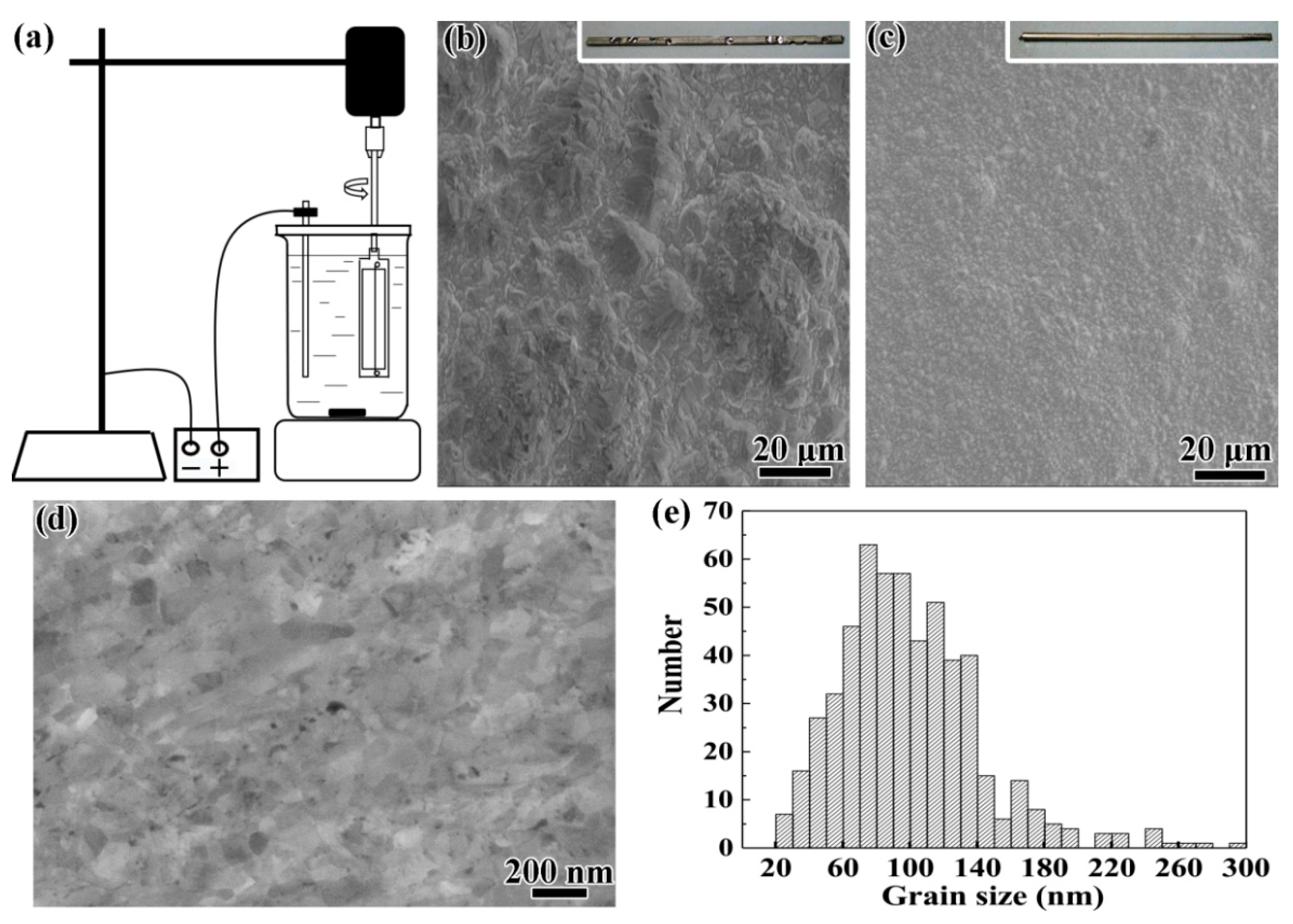
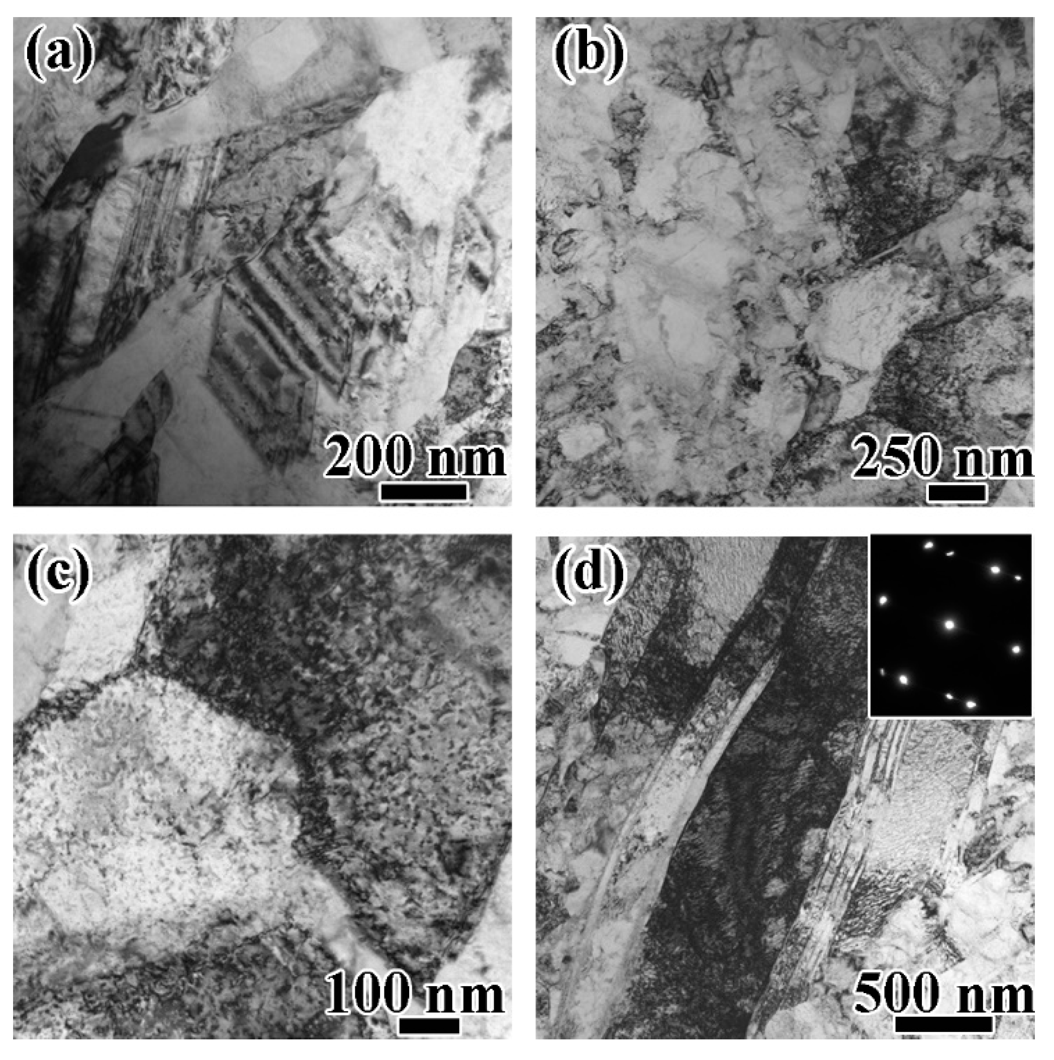
3.1. Microstructure
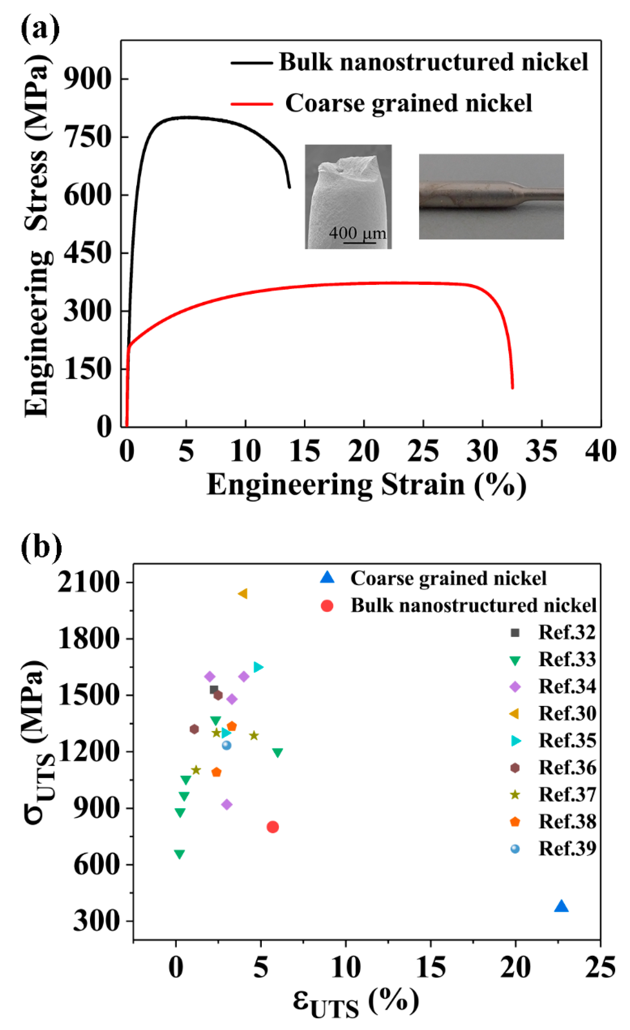
3.2. Mechanical Behaviours
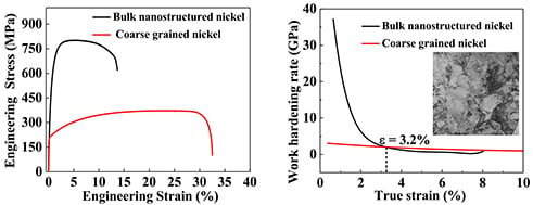
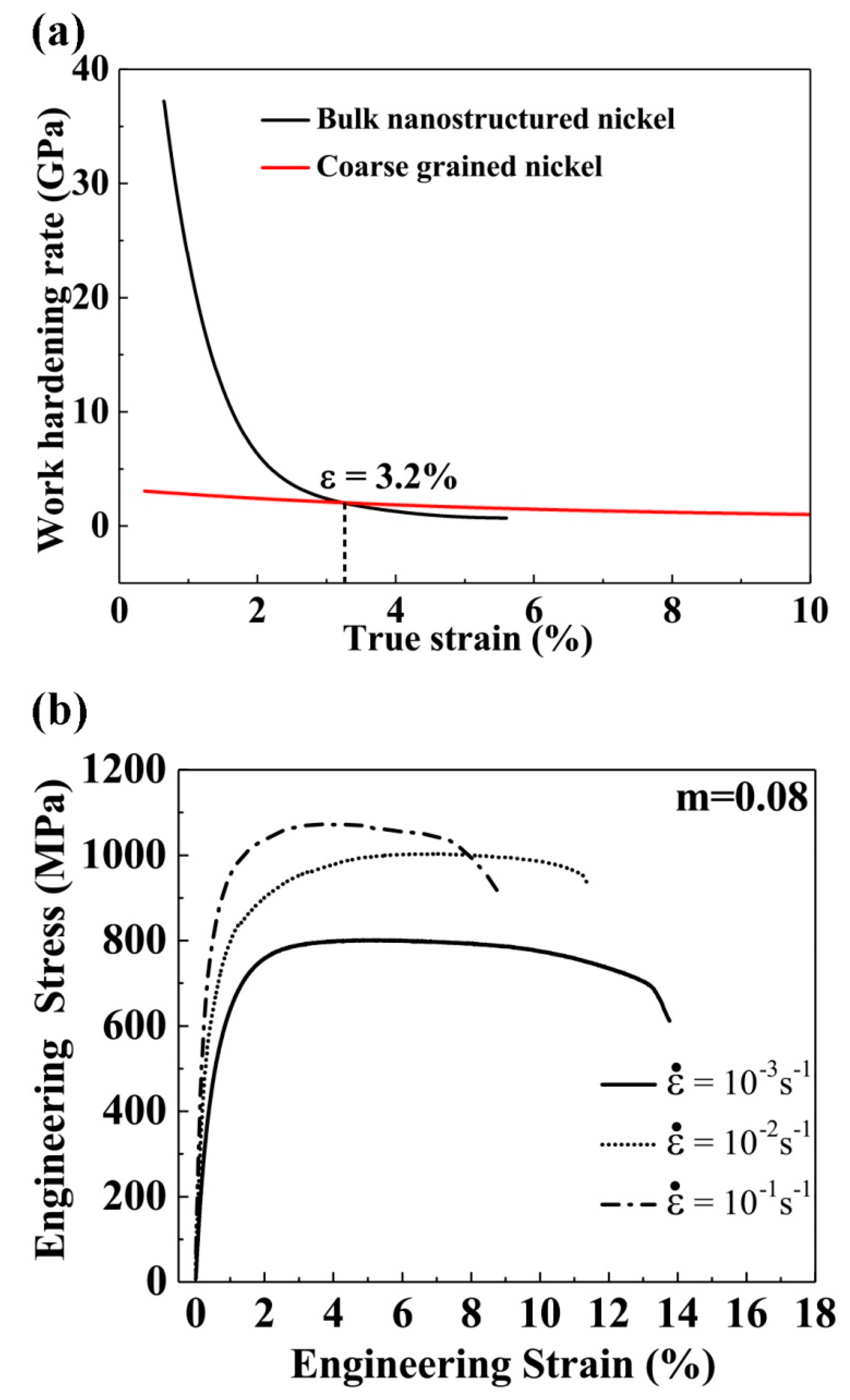
3.3. Work Hardening Rate
3.4. Deformation Mechanism
4. Discussion
5. Conclusions
Author Contributions
Funding
Conflicts of Interest
References
- Gleiter, H. Nanocrystalline materials. Prog. Mater. Sci. 1989, 33, 223–315. [Google Scholar] [CrossRef]
- El-Sherik, A.M.; Erb, U.; Palumbo, G.; Aust, K.T. Deviations from hall-petch behaviour in as-prepared nanocrystalline nickel. Scr. Mater. 1992, 27, 1185–1188. [Google Scholar] [CrossRef]
- Suryanarayana, C. Nanocrystalline materials. Int. Mater. Rev. 1995, 40, 41–64. [Google Scholar] [CrossRef]
- Erb, U. Electrodeposited nanocrystals: Synthesis, properties and industrial applications. Nanostruct. Mater. 1995, 6, 533–538. [Google Scholar] [CrossRef]
- Padmanabhan, K.A. Mechanical properties of nanostructured materials. Mater. Sci. Eng. A 2001, 304–306, 200–205. [Google Scholar] [CrossRef]
- Schuh, C.A.; Nieh, T.G.; Yamasaki, T. Hall–Petch breakdown manifested in abrasive wear resistance of nanocrystalline nickel. Scr. Mater. 2002, 46, 735–740. [Google Scholar] [CrossRef]
- Gertsman, V.Y.; Hoffmann, M.; Gleiter, H.; Birringer, R. The study of grain size dependence of yield stress of copper for a wide grain size range. Acta Mater. 1994, 42, 3539–3544. [Google Scholar] [CrossRef]
- Wang, Y.; Chen, M.; Zhou, F.; Ma, E. High tensile ductility in a nanostructured metal. Nature 2002, 419, 912–915. [Google Scholar] [CrossRef]
- Zhao, Y.; Topping, T.; Bingert, J.F.; Thornton, J.J.; Dangelewicz, A.M.; Li, Y.; Liu, W.; Zhu, Y.; Zhou, Y.; Lavernia, E.J. High Tensile Ductility and Strength in Bulk Nanostructured Nickel. Adv. Mater. 2008, 20, 3028–3033. [Google Scholar] [CrossRef]
- Erb, U.; Aust, K.T.; Palumbo, G. 6-Electrodeposited Nanocrystalline Metals, Alloys, and Composites. In Nanostructured Materials, 2nd ed.; Koch, C.C., Ed.; William Andrew Publishing: Norwich, NY, USA, 2007; pp. 235–292. [Google Scholar]
- McFadden, S.X.; Mishra, R.S.; Valiev, R.Z.; Zhilyaev, A.P.; Mukherjee, A.K. Low-temperature superplasticity in nanostructured nickel and metal alloys. Nature 1999, 398, 684–686. [Google Scholar] [CrossRef]
- Fecht, H.J.; Hellstern, E.; Fu, Z.; Johnson, W.L. Nanocrystalline metals prepared by high-energy ball milling. Metall. Trans. A 1990, 21, 2333–2337. [Google Scholar] [CrossRef]
- Valiev, R.Z.; Islamgaliev, R.K.; Alexandrov, I.V. Bulk nanostructured materials from severe plastic deformation. Prog. Mater. Sci. 2000, 45, 103–189. [Google Scholar] [CrossRef]
- Dao, M.; Lu, L.; Asaro, R.J.; De Hosson, J.T.M.; Ma, E. Toward a quantitative understanding of mechanical behavior of nanocrystalline metals. Acta Mater. 2007, 55, 4041–4065. [Google Scholar] [CrossRef]
- Chen, A.-Y.; Li, D.-F.; Zhang, J.-B.; Song, H.-W.; Lu, J. Make nanostructured metal exceptionally tough by introducing non-localized fracture behaviors. Scr. Mater. 2008, 59, 579–582. [Google Scholar] [CrossRef]
- Fang, T.H.; Li, W.L.; Tao, N.R.; Lu, K. Revealing Extraordinary Intrinsic Tensile Plasticity in Gradient Nano-Grained Copper. Science 2011, 331, 1587–1590. [Google Scholar] [CrossRef] [PubMed]
- Lu, K. Making strong nanomaterials ductile with gradients. Science 2014, 345, 1455–1456. [Google Scholar] [CrossRef]
- Wu, X.; Jiang, P.; Chen, L.; Yuan, F.; Zhu, Y.T. Extraordinary strain hardening by gradient structure. Proc. Natl. Acad. Sci. USA 2014, 111, 7197–7201. [Google Scholar] [CrossRef]
- Lu, K.; Lu, L.; Suresh, S. Strengthening Materials by Engineering Coherent Internal Boundaries at the Nanoscale. Science 2009, 324, 349–352. [Google Scholar] [CrossRef]
- Lu, L.; Shen, Y.; Chen, X.; Qian, L.; Lu, K. Ultrahigh Strength and High Electrical Conductivity in Copper. Science 2004, 304, 422–426. [Google Scholar] [CrossRef]
- Zhao, Y.H.; Liao, X.Z.; Cheng, S.; Ma, E.; Zhu, Y.T. Simultaneously Increasing the Ductility and Strength of Nanostructured Alloys. Adv. Mater. 2006, 18, 2280–2283. [Google Scholar] [CrossRef]
- Ovid'ko, I.A.; Valiev, R.Z.; Zhu, Y.T. Review on superior strength and enhanced ductility of metallic nanomaterials. Prog. Mater. Sci. 2018, 94, 462–540. [Google Scholar] [CrossRef]
- Injeti, G.; Leo, B. Electrodeposition of nanostructured coatings and their characterization—A review. Sci. Technol. Adv. Mater. 2008, 9, 043001. [Google Scholar] [CrossRef]
- Erb, U.; El-Sherik, A.M.; Palumbo, G.; Aust, K.T. Synthesis, structure and properties of electroplated nanocrystalline materials. Nanostruct. Mater. 1993, 2, 383–390. [Google Scholar] [CrossRef]
- Cziráki, Á.; Fogarassy, B.; Geröcs, I.; Tóth-Kádár, E.; Bakonyi, I. Microstructure and growth of electrodeposited nanocrystalline nickel foils. J. Mater. Sci 1994, 29, 4771–4777. [Google Scholar] [CrossRef]
- Lu, L.; Sui, M.L.; Lu, K. Superplastic Extensibility of Nanocrystalline Copper at Room Temperature. Science 2000, 287, 1463. [Google Scholar] [CrossRef]
- Maner, A.; Harsch, S.; Ehrfeld, W. Mass production of microstructures with extreme aspect ratios by electroforming. In Proceedings of the 74th AESF Annual Technical Conference (SUR/FIN'87), Chicago, IL, USA, 13–16 July 1987. [Google Scholar]
- Bacher, W.; Bade, K.; Matthis, B.; Saumer, M.; Schwarz, R. Fabrication of LIGA mold inserts. Microsyst. Technol. 1998, 4, 117–119. [Google Scholar] [CrossRef]
- Stark, W.; Matthis, B.; Saumer, M. Nickel sulphamate electrolytes for micro-electroforming. Galvanotechnik 1996, 87, 1107–1111. [Google Scholar]
- Schlesinger, M. Modern Electroplating, 5th ed.; John Wiley & Snos: Hoboken, NJ, USA, 2010; pp. 79–114. [Google Scholar]
- Hussain, I.; Jiang, Y.Y.; Jia, Y.D.; Wang, G.; Zhai, Q.J.; Chan, K.C.; Yi, J. Tensile behavior of Cu-coated Pd40Cu30Ni10P20 metallic glassy wire. Sci. Rep. 2018, 8, 5659. [Google Scholar] [CrossRef]
- Dalla Torre, F.; Van Swygenhoven, H.; Victoria, M. Nanocrystalline electrodeposited Ni: Microstructure and tensile properties. Acta Mater. 2002, 50, 3957–3970. [Google Scholar] [CrossRef]
- Dalla Torre, F.; Spätig, P.; Schäublin, R.; Victoria, M. Deformation behaviour and microstructure of nanocrystalline electrodeposited and high pressure torsioned nickel. Acta Mater. 2005, 53, 2337–2349. [Google Scholar] [CrossRef]
- Xiao, C.; Mirshams, R.A.; Whang, S.H.; Yin, W.M. Tensile behavior and fracture in nickel and carbon doped nanocrystalline nickel. Mater. Sci. Eng. A 2001, 301, 35–43. [Google Scholar] [CrossRef]
- Gu, C.; Lian, J.; Jiang, Z.; Jiang, Q. Enhanced tensile ductility in an electrodeposited nanocrystalline Ni. In Proceedings of the 2006 IEEE Conference on Emerging Technologies—Nanoelectronics, Singapore, 10–13 January 2006; pp. 293–297. [Google Scholar]
- Schwaiger, R.; Moser, B.; Dao, M.; Chollacoop, N.; Suresh, S. Some critical experiments on the strain-rate sensitivity of nanocrystalline nickel. Acta Mater. 2003, 51, 5159–5172. [Google Scholar] [CrossRef]
- Ebrahimi, F.; Ahmed, Z.; Li, H.Q. Tensile Properties of Electrodeposited Nanocrystalline FCC Metals. Mater. Manuf. Prog. 2006, 21, 687–693. [Google Scholar] [CrossRef]
- Shen, Y.F.; Xue, W.Y.; Wang, Y.D.; Liu, Z.Y.; Zuo, L. Mechanical properties of nanocrystalline nickel films deposited by pulse plating. Surf. Coat. Technol. 2008, 202, 5140–5145. [Google Scholar] [CrossRef]
- Ebrahimi, F.; Ahmed, Z. The effect of current density on properties of electrodeposited nanocrystalline nickel. J. Appl. Electrochem. 2003, 33, 733–739. [Google Scholar] [CrossRef]
- Ebrahimi, F.; Bourne, G.R.; Kelly, M.S.; Matthews, T.E. Mechanical properties of nanocrystalline nickel produced by electrodeposition. Nanostruc. Mater. 1999, 11, 343–350. [Google Scholar] [CrossRef]
- Wang, Y.M.; Cheng, S.; Wei, Q.M.; Ma, E.; Nieh, T.G.; Hamza, A. Effects of annealing and impurities on tensile properties of electrodeposited nanocrystalline Ni. Scr. Mater. 2004, 51, 1023–1028. [Google Scholar] [CrossRef]
- Hart, E.W. Theory of the tensile test. Acta Metall. 1967, 15, 351–355. [Google Scholar] [CrossRef]
- Youssef, K.M.; Scattergood, R.O.; Murty, K.L.; Horton, J.A.; Koch, C.C. Ultrahigh strength and high ductility of bulk nanocrystalline copper. Appl. Phys. Lett. 2005, 87, 091904. [Google Scholar] [CrossRef]
- Weibull, W.; Sweden, S. A Statistical Distribution Function of Wide Applicability. J. Appl. Mech. 1951, 18, 293–297. [Google Scholar] [CrossRef]
- Ashby, M.F. The deformation of plastically non-homogeneous materials. Philos. Mag. 1970, 21, 399–424. [Google Scholar] [CrossRef]
- Chakravarthy, S.S.; Curtin, W.A. Stress-gradient plasticity. Proc. Natl. Acad. Sci. USA 2011, 108, 15716–15720. [Google Scholar] [CrossRef] [PubMed]


© 2019 by the authors. Licensee MDPI, Basel, Switzerland. This article is an open access article distributed under the terms and conditions of the Creative Commons Attribution (CC BY) license (http://creativecommons.org/licenses/by/4.0/).
Share and Cite
Jiang, Y.; Yi, J.; Hu, K.; Zhao, J.; Huang, B.; Jia, Y.; Wang, G. Strong and Ductile Electroplated Heterogeneous Bulk Nanostructured Nickel. Materials 2019, 12, 1573. https://doi.org/10.3390/ma12101573
Jiang Y, Yi J, Hu K, Zhao J, Huang B, Jia Y, Wang G. Strong and Ductile Electroplated Heterogeneous Bulk Nanostructured Nickel. Materials. 2019; 12(10):1573. https://doi.org/10.3390/ma12101573
Chicago/Turabian StyleJiang, Yaoyao, Jun Yi, Kai Hu, Jing Zhao, Bo Huang, Yandong Jia, and Gang Wang. 2019. "Strong and Ductile Electroplated Heterogeneous Bulk Nanostructured Nickel" Materials 12, no. 10: 1573. https://doi.org/10.3390/ma12101573
APA StyleJiang, Y., Yi, J., Hu, K., Zhao, J., Huang, B., Jia, Y., & Wang, G. (2019). Strong and Ductile Electroplated Heterogeneous Bulk Nanostructured Nickel. Materials, 12(10), 1573. https://doi.org/10.3390/ma12101573