Article

In-Situ and Ex-Situ Characterization of Femtosecond Laser-Induced Ablation on As2S3 Chalcogenide Glasses and Advanced Grating Structures Fabrication

1
Laboratory of Infrared Materials and Devices, The Research Institute of Advanced Technologies, Ningbo University, Ningbo 315211, China
2
College of Mechanical and Electronic Engineering, Chaohu University, Hefei 230000, China
*
Authors to whom correspondence should be addressed.
Materials 2019, 12(1), 72; https://doi.org/10.3390/ma12010072
Submission received: 11 November 2018 / Revised: 20 December 2018 / Accepted: 21 December 2018 / Published: 26 December 2018
(This article belongs to the Section Optical and Photonic Materials)

Abstract

:
Femtosecond laser pulse of 800 nm wavelength and 150 fs temporal width ablation of As2S3 chalcogenide glasses is investigated by pump-probing technology. At lower laser fluence (8.26 mJ/cm2), the surface temperature dropping to the melting point is fast (about 43 ps), which results in a clean hole on the surface. As the laser fluence increases, it takes a longer time for lattice temperature to cool to the melting point at high fluence (about 200 ps for 18.58 mJ/cm2, about 400 ps for 30.98 mJ/cm2). The longer time of the surface heating temperature induces the melting pool in the center, and accelerates material diffusing and gathering surrounding the crater, resulting in the peripheral rim structure and droplet-like structure around the rim. In addition, the fabricated long periodic As2S3 glasses diffraction gratings can preserve with high diffraction efficiency by laser direct writing technology.

1. Introduction

Chalcogenide glasses (ChGs) have gained extensive interest due to its wide transparency range, high refractive index, high nonlinear optical coefficient and high photosensitivity [1,2,3,4]. In this case, ChGs can be used as excellent candidate materials for optical communication, optical sensing and optical recording areas [5,6]. In particular, the generation in surface nano-structures and nanohole arrays or nano-gratings with the largest achievable manipulation of refractive index, master the key to functional devices in future optical systems [7,8,9]. Among these manufacturing technologies, femtosecond lasers has opened up new applications and possibilities in the bulk glass materials due to its limited heat affected zone, very high flexibility and noncontact process, which has been used in the manufacturing of Nd:LuVO4, Ge-Sb-Se,As2Se3, Tm:YVO4 and Nd:GLSG (neodymium doped gallium lanthanum sulfide glass) [10,11,12,13,14]. Femtosecond direct writing methods in the case of chalcogenide bulk glass and fibers have been used to make 3D holographic recordings, bulks of gratings and waveguides [15,16,17,18]. In addition, long-period gratings are an important part of optical communication systems for optical filtering and mode conversion, optical gain, and sensing applications. [19,20]. For example, the long periodic gratings have nonlinear periodic structure embodiment; in this condition, the nonlinear refractive index is used as optical switching devices [21].
Basic understanding of the process of femtosecond laser-induced material changes is important for the prediction and optimization of laser processes [22,23]. At present, optical detection technology has been used in laser–material interaction research [24,25]. For example, Pump-probing and time-resolved shadow-graphics techniques have been used to directly observe ablation processes in very short (picosecond) timescale [26,27,28,29]. At present, there were few studies on the surface morphology evolution of femtosecond laser-induced chalcogenide glass materials, and the mechanism of the surface morphology evolution is still not perfectly explained. Nevertheless, even in the simplest case of chalcogenide materials, such as As2S3 and As2Se3, the femtosecond laser-induced process of phase change and the ablation have not been investigated. What is more important is that basic understanding of the process of femtosecond laser-induced processes is important for the prediction of laser manufacturing.
In this letter, we study the evolution process of surface morphology of femtosecond laser-induced As2S3 chalcogenide glasses, and the basic structural property of the As2S3 has been reported in some references [30]. We have carried out pump-probing technology to investigate the femtosecond laser-induced ablation processes in As2S3 glass. The pump-probing setup elucidates the transient breakup of the edge rim, droplet-like and ablation area. By studying the relationship between the surface morphologies and the laser fluences, we can fabricate a long-period grating structure with smooth morphology on the surface of As2S3.

2. Materials and Methods

The pump-probing setup revealed the evolution of different morphologies during the ablation processes. The pump-probing imaging system was set up as shown in Figure 1. Ti Sapphire laser pulses of 800 nm wavelength and 150 fs temporal width impinged As2S3 targets. The laser beam was focused by a × 5 corrected, non-achromatic long working distance objective lens at normal incidence. For the reflection probing system, the 632.8 nm He-Ne continuous laser has been focused onto the center of the irradiated region at normal incidence. The As2S3 specimens are positioned at the focal plane of the probing laser whose location is defined by knife-edge beam profiling. The laser processing beam and probe beam are also measured under the knife-edge method. The intensity of the reflection probe signal was measured by a fast photodiode coupled to an oscilloscope. The oscilloscope is used to record the actual delay time of the processing laser signal and the probing laser signal. To ensure true representation, at least four signals are examined at each delay setting.

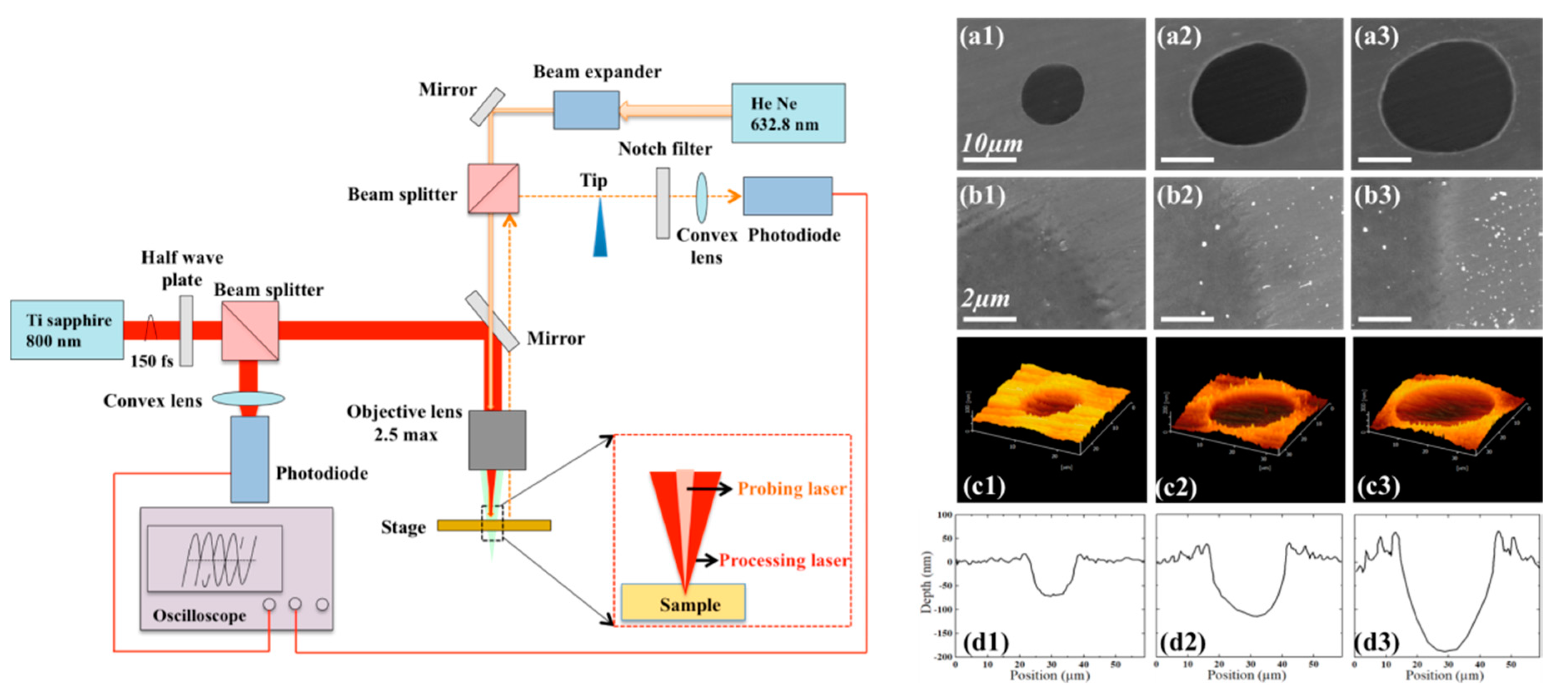
3. Results and Discussion

Typical submicron-scale structures are shown in SEM and AFM images. Smooth crater structures can be formed after irradiation of laser at lower laser fluence (8.26 mJ/cm2) on As2S3 glass surface, and rim structure around the crater appears as the increasing of the laser fluences, as shown in Figure 1(a1–a3). Figure 1(b1–b3) give detailed information of edges of the surface crater structures, and the outer edge is relatively smooth at low laser fluence (8.26 mJ/cm2). As the fluence of laser increases to 18.58mJ/cm2, rim structure combined with some droplet-like structures on the edge appear, and the size of these droplet-like structures grows bigger around the crater outskirt as the increasing of the laser fluence (30.98 mJ/cm2). The detailed crossing-sectional characters of the crater structures are measured by the AFM images. At higher laser fluence, as shown in Figure 1(d1–d3), the rim structure round the crater appears and the height of the rims becomes larger.
Next, the detailed relationship between the characters of the surface craters and the laser fluences are investigated, which is shown in Figure 2. The red data points show the measured crater depth as a function of fluence, and the red curve is the corresponding simulated result. For the femtosecond laser irradiation, the OPA (one-photon absorption) should be taken into account to explain the ablation depth. Besides, laser fluences described by a Lambert–Beer, the balance equation for carrier number density N, the complex refractive index n of the material should be considered [31]:
Lambert–Beer law:
I z = ( α 0 + α D r u d e ) I β I 2
Carrier number density N of the balance equation:
N t + ( D 0 N ) = α 0 I h ω + β I 2 2 h ω
The complex refractive index n is calculated by the Drude model:
n = ε A s 2 S 3 ω p 2 ω 2 + i ω / τ d
In Equation (1), I = (1 − R)I0, R is the surface reflectivity. For the As2S3 materials, the OPA coefficient α0~103/cm [32,33,34], ε A s 2 S 3 is the dielectric constant of As2S3 [35], ω is the angular frequency of the pulse, and τ d is the damping time (1.1 fs). The plasma frequency ωp = (4πNe2/m*)1/2, and electron effective mass m* = 0.18 me. The absorption of the incident laser in the plasma αDrude = 4πk/λ, D0 is the coefficient of ambipolar diffusivity (18 cm2/s) and h ω is the photon energy. A single shot ablation threshold Fth = 7.21 mJ/cm2 can be measured. In addition, we also determine Fth by measuring the crater diameter D for different laser fluences and by using the linear relationship D2 = 2rf2[ln(F) − ln(Fth)] [36], where the 1/e beam radius, rf, is about 18 μm. The black data points show the hole diameter as a function of laser intensity, and the As2S3 ablation threshold (Fth) is estimated as 7.19 mJ/cm2, which is consistent with the former result (Fth = 7.21 mJ/cm2). Finally, the aspect ratio (color in blue), the crater diameter divide by the depth, is also described. As the laser pulse energy increases, the aspect ratio first increases and then decreases. The largest aspect ratio is 156 at 12.39 mJ/cm2 of laser fluence, which is related to the competition mechanism between the melting depth and Gaussian laser beam distribution, and the melting depth grows directly with the laser fluence and reaches the saturation state [37].
The reflection probing reveals the transient dynamics of laser interaction with As2S3, which is shown in Figure 3. The drop in low fluence can be concluded as the effect of the ablation since the ablation gives a crater in the irradiation area, indicating a weaker reflection. And under high fluence pump laser irradiation, the reflections directly drop to a lower state. Therefore, the reflection measurement validates the dynamics of ablation processing. Besides, the trends of the surface temperature after laser irradiation are also investigated, as shown in Figure 3. The energy conversion follows a one-dimensional dual temperature model which was proposed by Qiu and Tien [38].
C e t T e = t k x T e G ( T e T l ) + S
C l t T l = G ( T e T l )
S = 0.94 1 R t p δ J exp [ x δ 2.77 ( t t p ) 2 ]
In this equation, Ce, is the electron heat capacity and Cl is the lattice heat capacity. G is the electron-lattice coupling factor, S is the radiation heating source term, and R is the reflectivity, δ is the radiation penetration depth, J is the energy of laser pulse [39]. All the material simulated is As2S3 glass and its physical constants are listed in Table 1, and the initial and boundary conditions for both the electron and the lattice systems can be defied as T e ( x , 2 t p ) =   T l ( x , 2 t p ) = T 0 . At low laser fluences, the energy of these heated electrons can be transferred to the surrounded lattice very rapidly (several picoseconds), as shown in Figure 4.
We can find that the surface temperature reaches a maximum value of 697 K at 6 ps, and the melting depth is 68 nm when the laser fluence is 8.26 mJ/cm2. With the increase of laser fluence, the surface temperature can reach 969 K and 1246 K after 7 and 8 ps laser irradiation, as shown in Figure 4. Besides, the melting depths are 161 nm and 252 nm, respectively. The depths obtained by experiments at the same three fluences are 72 nm, 162 nm and 262 nm, which are consistent with the theory results. For the different laser fluences, it takes about 43 ps, 173 ps and 450 ps for the temperature dropping to the melting point of the material, which is consistent with reflection probing experimental results, as shown in Figure 3.
At lower laser fluence, as shown in Figure 3, and the non-thermal mechanisms play a major role for the laser–materials processing, which results in a clean hole on the surface. As the laser fluence increases, firstly, lattice temperature reaches a maximum (7 ps) and then the lattice temperature begins to gradually decline. Since it takes longer for the lattice temperature to drop to the material melting point at high fluence, with increasing laser fluence, it takes much longer for the surface temperature to drop to the melting temperature, which is due to the theory of the one-dimensional dual temperature model. In this condition, the laser is the only heating source and the higher laser fluence induces the higher surface temperature; it takes more time to diffuse the surface heat. The material surface reflectivity decreases more slowly (about 200 ps for 18.58 mJ/cm2 in Figure 3). The time of the surface heating temperature can reach 200 ps or above, causing the melting pool in the center, resulting in the material diffuses and gathers surround the crater. For higher laser fluence (above 30.98 mJ/cm2), the liquid As2S3 materials are rapidly pulled out of the pool, resulting the peripheral rim structures.
The former results show that holes can be fabricated at the fluence of 8.26 mJ/cm2. In addition, direct laser writing (DLW) in processing is a fast and flexible method for long periodic grating fabrication [29]. Figure 5 shows the laser direct writing single gratings (a–c) and the composite gratings (d–f) at the laser scanning velocity of 1, 2 and 5 mm/s, respectively. In the optical microscope pattern, black color areas are the laser direct writing areas, and gray areas are single grating (a1–c1) and the composite grating structures (d1–f1) with a period of 48, 35 and 20μm, respectively. The depths of these gratings are about 3.8, 2.6, 1.1 μm, respectively. For the lower scanning velocity, the morphology of the gratings is not perfect, which result from the multiple-pulse laser acting on the surface, and thereby forming some rim structure around the grating, as shown in Figure 5(a2,d2). For the larger scanning velocity, it is equivalent to a single-pulse laser irradiation effect, and wrinkled structures are formed around the grating, as shown in Figure 5(c1,f1).
In order to investigate the quality of the grating, we measured the diffraction efficiency of single gratings, as shown in Figure 5(a3–c3) and composite gratings (d3–f3). The laser fluence of the light source with a wavelength of 632.8 nm is 2.3 mw and the distance between the grating and the screen is 60 cm, and the incident angle of the laser through the grating is θ = 0°. The diffraction efficiency of long periodic gratings is η + 1 = 3.48% for d = 20 μm, η + 1 = 6.30% for d = 35 μm, and η + 1 = 5.74% for d = 48 μm. And, efficiency values of (η + 2) are 0.91%, 1.71%, and 1.52%, respectively. The diffraction efficiency of composite gratings is η + 1 = 1.74% for d = 20 μm, η + 1 = 3.17% for d = 35 μm, and η + 1 = 2.70% for d = 48 μm. The diffraction efficiency of the grating increases first and then decreases with the increases of laser scanning velocity, which results from the morphologies of the grating structures. The diffraction efficiency of the grating increases and then decreases with the increases of laser scanning velocity, which results from the morphologies of the grating structures. The grating structures with such wrinkled or rim structures around gratings and the photo-darkening process [43,44] can scatter or absorb the incident light, finally reducing the diffraction efficiency of the grating structures. In this condition, the long periodic gratings on As2S3 glasses surface can preserve high diffraction efficiency with a wide range (0.6–8 μm).

4. Conclusions

In conclusion, we have carried out pump-probing technology to investigate the femtosecond laser-induced ablation processes in As2S3 glass. The pump-probing setup elucidates the transient breakup of the edge rim, droplet-like and ablation area. Besides, diffraction gratings with period of 20, 35, and 48 μm on the As2S3 chalcogenide glass surface are fabricated with different laser scanning velocity. And the first-order diffraction efficiency of the gratings to be up to 6.3% at λ (632.8 nm) with transmittance operation at normal incidence can be fabricated at a proper laser scanning velocity and laser fluence.

Author Contributions

Data curation, H.W.; Formal analysis, H.W.; Funding acquisition, D.Q.; Investigation, Z.Z., Y.Z., T.X., X.Z., S.D., X.S., B.S., P.Z. and Y.X.; Project administration, D.Q.; Software, H.W.; Supervision, X.Y.

Funding

Acknowledge the Natural Science Foundation of China (61705117), and thank the support of the Key Research and Development Program of Zhejiang Province (2017C01005), and Anhui Provincial Natural Science Foundation under Grant 1808085QF216. And acknowledge the support of 3315 innovation team, Ningbo city. It was also support by K.C. Wong Magna Fund in Ningbo University.

Conflicts of Interest

The authors declare no conflict of interest.

References

  1. Smektala, F.; Quemard, C.; Leneindre, L.; Lucas, J.; Barthélémy, A.; Angelis, C.D. Chalcogenide glasses with large non-linear refractive indices. J. Non-Cryst. Solids 1998, 239, 139–142. [Google Scholar] [CrossRef]
  2. Petkov, K.; Ewen, P.J.S. Photoinduced changes in the linear and non-linear optical properties of chalcogenide glasses. J. Non-Cryst. Solids 1999, 249, 150–159. [Google Scholar] [CrossRef]
  3. Sanghera, J.S.; Shaw, L.B.; Aggarwal, I.D. Chalcogenide Glass-Fiber-Based Mid-IR Sources and Applications. IEEE J. Sel. Top. Quantum Electron. 2009, 15, 114–119. [Google Scholar] [CrossRef]
  4. Shimakawa, K.; Kolobov, A.; Elliott, S.R. Photoinduced effects and metastability in amorphous semiconductors and insulators. Adv. Phys. 1995, 44, 475–588. [Google Scholar] [CrossRef]
  5. Marie-Laure, A.; Julie, K.; Virginie, N.; Koji, H.; Satoru, I.; Catherine, B.P.; Hervé, L.; Joël, C.; Kiyoyuki, Y.; Olivier, L. Chalcogenide Glass Optical Waveguides for Infrared Biosensing. Sensors 2009, 9, 7398–7411. [Google Scholar] [Green Version]
  6. Madden, S.J.; Choi, D.; Bulla, D.A.; Rode, A.V.; Lutherdavies, B.; Ta’Eed, V.G.; Pelusi, M.D.; Eggleton, B.J. Long, low loss etched As2S3 chalcogenide waveguides for all-optical signal regeneration. Opt. Express 2007, 15, 14414–14421. [Google Scholar] [CrossRef] [PubMed]
  7. Wang, L.; Rho, Y.; Shou, W.; Hong, S.; Kato, K.; Eliceiri, M.; Shi, M.; Grigoropoulos, C.P.; Pan, H.; Carraro, C. Programming Nanoparticles in Multiscale: Optically Modulated Assembly and Phase Switching of Silicon Nanoparticle Array. ACS Nano 2018, 12, 2231. [Google Scholar] [CrossRef] [PubMed]
  8. Qi, D.; Tang, S.; Wang, L.; Dai, S.; Shen, X.; Wang, C.; Chen, S. Pulse laser-induced size-controllable and symmetrical ordering of single-crystal Si islands. Nanoscale 2018, 10, 8133–8138. [Google Scholar] [CrossRef] [PubMed]
  9. Zhang, Q.; Lin, H.; Jia, B.; Xu, L.; Gu, M. Nanogratings and nanoholes fabricated by direct femtosecond laser writing in chalcogenide glasses. Opt. Express 2010, 18, 6885–6890. [Google Scholar] [CrossRef]
  10. Velea, A.; Popescu, M.; Sava, F.; Lorinczi, A.; Simandan, I.D.; Socol, G.; Mihailescu, I.N.; Stefan, N.; Jipa, F.; Zamfirescu, M. Photoexpansion and nano-lenslet formation in amorphous As2S3 thin films by 800 nm femtosecond laser irradiation. J. Appl. Phys. 2012, 112, 499. [Google Scholar] [CrossRef]
  11. You, C.; Dai, S.; Zhang, P.; Xu, Y.; Wang, Y.; Xu, D.; Wang, R. Mid-infrared femtosecond laser-induced damages in As2S3 and As2Se3 chalcogenide glasses. Sci. Rep. 2017, 7, 6497. [Google Scholar] [CrossRef] [PubMed]
  12. Cumming, B.P.; Debbarma, S.; Luther-Davies, B.; Gu, M. Effect of refractive index mismatch aberration in arsenic trisulfide. Appl. Phys. B 2012, 109, 227–232. [Google Scholar] [CrossRef]
  13. Blackburn, D.H.; Osmalov, J.S. Properties of arsenic sulfide glass. J. Res. Natl. Bur. Stand. 1957, 59, 2774. [Google Scholar]
  14. Richardson, M.C.; Zoubir, A.; Rivero, C.; Lopez, C.; Petit, L.C.; Richardson, K.A. Femtosecond laser microstructuring and refractive index modification applied to laser and photonic devices. Proc. SPIE–Int. Soc. Opt. Eng. 2004, 5347, 18–27. [Google Scholar]
  15. Juodkazis, S.; Rode, A.V.; Matsuo, S. Three-dimensional recording and structuring of chalcogenide glasses by femtosecond pulses. Int. Symp. Laser Precis. Microfabr. 2004, 5662, 179–184. [Google Scholar]
  16. Mihailov, S.J.; Dan, G.; Smelser, C.W.; Lu, P.; Walker, R.B.; Ding, H. Bragg grating inscription in various optical fibers with femtosecond infrared lasers and a phase mask. Opt. Mater. Express 2011, 1, 754–765. [Google Scholar] [CrossRef]
  17. Kohoutek, T.; Hughes, M.A.; Orava, J.; Mastumoto, M.; Misumi, T.; Kawashima, H.; Suzuki, T.; Ohishi, Y. Direct laser writing of relief diffraction gratings into a bulk chalcogenide glass. J. Opt. Soc. Am. B 2012, 29, 2779. [Google Scholar] [CrossRef]
  18. Hughes, M.; Yang, W.; Hewak, D. Fabrication and characterization of femtosecond laser written waveguides in chalcogenide glass. Appl. Phys. Lett. 2007, 90, 704. [Google Scholar] [CrossRef]
  19. James, S.W.; Tatam, R.P. Optical fibre long-period grating sensors: characteristics and application. Meas. Sci. Technol. 2003, 14, 49–61. [Google Scholar] [CrossRef]
  20. Pudo, D.; Mägi, E.C.; Eggleton, B.J. Long-period gratings in chalcogenide fibers. Opt. Express 2006, 14, 3763–3766. [Google Scholar] [CrossRef]
  21. Finsterbusch, K.; Baker, N.; Ta’Eed, V.G.; Eggleton, B.J.; Choi, D.; Madden, S.; Lutherdavis, B. Long-period gratings in chalcogenide rib waveguides. Electron. Lett. 2006, 42, 1094–1095. [Google Scholar] [CrossRef]
  22. Rebollar, E.; Vázquez de Aldana, J.R.; Pérez-Hernández, J.A.; Ezquerra, T.A.; Moreno, P.; Castillejo, M. Ultraviolet and infrared femtosecond laser induced periodic surface structures on thin polymer films. Appl. Phys. Lett. 2012, 100, 041106. [Google Scholar] [CrossRef] [Green Version]
  23. Favazza, C.; Kalyanaraman, R.; Sureshkumar, R. Robust nanopatterning by laser-induced dewetting of metal nanofilms. Nanotechnology 2006, 17, 4229. [Google Scholar] [CrossRef] [PubMed]
  24. Hono, K.; Ohkubo, T.; Chen, Y.M.; Kodzuka, M.; Ohishi, K.; Sepehriamin, H.; Li, F.; Kinno, T.; Tomiya, S.; Kanitani, Y. Broadening the applications of the atom probe technique by ultraviolet femtosecond laser. Ultramicroscopy 2011, 111, 576–583. [Google Scholar] [CrossRef] [PubMed]
  25. Greenfield, M.; Guo, Y.Q.; Bernstein, E.R. Ultrafast photodissociation dynamics of HMX and RDX from their excited electronic states via femtosecond laser pump–probe techniques. Chem. Phys. Lett. 2006, 430, 277–281. [Google Scholar] [CrossRef]
  26. Mouskeftaras, A.; Guizard, S.; Fedorov, N.; Klimentov, S. Mechanisms of femtosecond laser ablation of dielectrics revealed by double pump–probe experiment. Appl. Phys. A 2013, 110, 709–715. [Google Scholar] [CrossRef]
  27. Qi, D.; Zhang, Z.; Yu, X.; Zhang, Y. Visualization of nanosecond laser-induced dewetting, ablation and crystallization processes in thin silicon films. Phys. Lett. A 2018, 1540–1544. [Google Scholar] [CrossRef]
  28. Zhang, N.; Zhu, X.; Yang, J.; Wang, X.; Wang, M. Time-resolved shadowgraphs of material ejection in intense femtosecond laser ablation of aluminum. Phys. Rev. Lett. 2007, 99, 167602. [Google Scholar] [CrossRef]
  29. Qi, D.; Paeng, D.; Yeo, J.; Kim, E.; Wang, L.; Chen, S.; Grigoropoulos, C.P. Time-resolved analysis of thickness-dependent dewetting and ablation of silver films upon nanosecond laser irradiation. Appl. Phys. Lett. 2016, 108, 193. [Google Scholar] [CrossRef]
  30. Georgescu, G.; Sava, F.; Rares-Medianu, M. Structure of bulk glassy As2Se3 and As2S3. J. Optoelectron. Adv. Mater. 2006, 8, 1801–1805. [Google Scholar]
  31. Zhang, H.; Oosten, D.V.; Krol, D.M.; Dijkhuis, J.I. Saturation effects in femtosecond laser ablation of silicon-on-insulator. Appl. Phys. Lett. 2011, 99, 214101. [Google Scholar] [CrossRef]
  32. Shaaban, E.R. Optical characterization of arsenic sulfide semiconducting glass films using the transmittance measurements. Mater. Chem. Phys. 2006, 100, 411–417. [Google Scholar] [CrossRef]
  33. Marquez, E.; Ramirezmalo, J.; Villares, P.; Jimenezgaray, R.; Ewen, P.J.S.; Owen, A.E. Calculation of the thickness and optical constants of amorphous arsenic sulphide films from their transmission spectra. J. Phys. D Appl. Phys. 2000, 139, 535. [Google Scholar] [CrossRef]
  34. Kosa, T.I.; Rangel-Rojo, R.; Hajto, E.; Ewen, P.J.S.; Owen, A.E.; Kar, A.K.; Wherrett, B.S. Nonlinear optical properties of silver-doped As2S3. J. Non-Cryst. Solids 1993, 164–166, 1219–1222. [Google Scholar] [CrossRef]
  35. Synowicki, R.A.; Tiwald, T.E. Optical properties of bulk c-ZrO2, c-MgO and a-As2S3 determined by variable angle spectroscopic ellipsometry. Thin Solid Films 2004, 455, 248–255. [Google Scholar] [CrossRef]
  36. Jandeleit, J.; Urbasch, G.; Hoffmann, H.D.; Treusch, H.G.; Kreutz, E.W. Picosecond laser ablation of thin copper films. Appl. Phys. A 1996, 63, 117–121. [Google Scholar] [CrossRef]
  37. Krause, S.; Miclea, P.T.; Steudel, F.; Schweizer, S.; Seifert, G. Precise microstructuring of indium-tin oxide thin films on glass by selective femtosecond laser ablation. EPJ Photovolt. 2013, 4, 40601. [Google Scholar] [CrossRef] [Green Version]
  38. Qiu, T.Q.; Tien, C.L. Femtosecond laser heating of multi-layer metals—I. Analysis. Int. J. Heat Mass Transf. 1994, 37, 2789–2797. [Google Scholar] [CrossRef]
  39. Sanghera, J.S.; Aggarwal, I.D. Active and passive chalcogenide glass optical fibers for IR applications: A review. J. Non-Cryst. Solids 1999, 256–257, 6–16. [Google Scholar] [CrossRef]
  40. Espeau, P.; Tamarit, J.L.; Barrio, M.; López, D.Ó.; Perrin, M.A.; Allouchi, H.; Céolin, R. Solid State Studies on Synthetic and Natural Crystalline Arsenic(III) Sulfide, As2S3 (Orpiment):  New Data for an Old Compound. Chem. Mater. 2006, 18, 3821–3826. [Google Scholar] [CrossRef]
  41. Sheng, W.W.; Westgate, C.R. On the preswitching phenomena in semiconducting glasses. Solid State Commun. 1971, 9, 387–391. [Google Scholar] [CrossRef]
  42. Hattori, M.; Nagaya, K.; Umebachi, S.; Tanaka, M. Heat capacities of AsS glasses. J. Non-Cryst. Solids 1970, 3, 195–204. [Google Scholar] [CrossRef]
  43. Juodkazis, S.; Misawa, H.; Louchev, O.A.; Kitamura, K. Femtosecond laser ablation of chalcogenide glass: Explosive formation of nano-fibres against thermo-capillary growth of micro-spheres. Nanotechnology 2006, 17, 4802–4805. [Google Scholar] [CrossRef]
  44. Juodkazis, S.; Kondo, T.; Misawa, H.; Rode, A.; Samoc, M.; Luther-Davies, B. Photo-structuring of As2S3 glass by femtosecond irradiation. Opt. Express 2006, 14, 7751–7756. [Google Scholar] [CrossRef] [PubMed]
Figure 1. The left image, pump-probing setup of femtosecond laser-induced in As2S3, and the fullwidthathalfmaximum (FWHM) of pump laser and probing laser are 36 μm and 20 μm, respectively. (a1)–(a3) The right image, scanning electron microscopy; (b1)–(b3) the magnified SEM images; (c1)–(c3) AFM images; (d1)–(d3) and the cross-sections AFM images. Irradiation laser flences: 8.26 mJ/cm2, 18.58 mJ/cm2 and 30.98 mJ/cm2, respectively.
Materials 12 00072 g001
Figure 2. (a) The ablation diameter of ra2, versus the laser fluence ln(F). (b) The data points in red, black and blue indicate the hole depth, the diameter and the corresponding aspect ratio, respectively, the red solid curve, the black solid curve and the blue solid curve show the calculated hole depth, the diameter and the aspect ratio using a 150-fs pulse duration laser, respectively.
Materials 12 00072 g002
Figure 3. The pump-probing reflectivity signals of laser-induced ablation of As2S3 with different laser fluences in scatter-lines, and the corresponding simulated surface temperature as a relationship of time for the applied incident laser intensity in solid lines.
Materials 12 00072 g003
Figure 4. The relationship between surface temperature and depth of the material at different delay times, (a) 8.26 mJ/cm2, (b) 18.58 mJ/cm2, (c) 30.98 mJ/cm2, respectively.
Materials 12 00072 g004
Figure 5. The laser energy was 8.26 mJ/cm2, the scanning speed were 1, 2 and 5 mm/s, and the corresponding period were 48, 35 and 20μm single gratings (ac) and composite gratings (df). (a1f1) were the pattern of optical microscope, (a2f2) were the step meter profile, and (a3f3) were the grating diffraction pattern.
Materials 12 00072 g005aMaterials 12 00072 g005b
Table 1. Parameters forAs2S3 used in heat calculation [38,39,40,41,42].
As2S3 (Parameters)Values
Initial temperature (T0)300 K
Thermal conductivity (k)0.17 W·m−1·C−1
Lattice heat capacity (Ci)1 × 10⁶ J·m−3·K−1
Electron heat capacity (Ce)502 J·Kg−1·K−1
Electron-phonon coupling factor (G)2.6 × 10¹⁶ W·m−3·K−1
Reflection coefficient (R)0.6
Radiation penetration depth (δ)15.3 nm

