Article

Research on the Factors Affecting the Growth of Large-Size Monolayer MoS2 by APCVD

1
Key Laboratory for Wide-Band Gap Semiconductor Materials and Devices of Education, School of Microelectronics, Xidian University, Xi’an 710071, China
2
The School of Mathematics and Statistics, Xidian University, Xi’an 710071, China
*
Authors to whom correspondence should be addressed.
Materials 2018, 11(12), 2562; https://doi.org/10.3390/ma11122562
Submission received: 16 November 2018 / Revised: 10 December 2018 / Accepted: 14 December 2018 / Published: 17 December 2018

Abstract

:
The transition-metal chalcogenides (TMDs) are gaining increased attention from many scientists recently. Monolayer MoS2 is an emerging layered TMD material with many excellent physical and electrical properties. It can be widely used in catalysis, transistors, optoelectronics and integrated circuits. Here, the large-sized monolayer MoS2 is grown on the silicon substrate with a 285-nm-thick oxide layer by atmospheric pressure chemical vapor deposition (APCVD) of sulfurized molybdenum trioxide. This method is simple and it does not require vacuum treatment. In addition, the effects of growth conditions, such as sulfur source, molybdenum source, growth temperature, and argon flow rate on the quality and area of MoS2 are further studied systematically. These analysis results help to master the morphology and optical properties of monolayer MoS2. The high quality, excellent performance, and large-size monolayer MoS2 under the optimal growth condition is characterized by optical microscopy, AFM, XPS, photoluminescence, and Raman spectroscopy. The Raman spectrum and PL mapping show that the grown MoS2 is a uniform triangular monolayer with a side length of 100 μm, which can pave the way for the applications of photodetectors and transistors.

1. Introduction

In recent years, two-dimensional materials have been a hot topic in Nano-electronic research [1,2,3]. Many scientists have conducted extensive research on graphene with ultra-thin, ultra-strong and super-conductive properties. The pristine graphene has no band gap, so it cannot be used in the logic circuits. To compensate for the lack of band gap in graphene, researchers have begun to focus on the monolayer MoS2 with its graphene-like structure [4]. Monolayer MoS2 has a sandwich layered structure, the upper and lower layers are hexagonal planes composed of sulfur atoms, and the middle is a metal molybdenum atomic layer [5]. The atoms in monolayer MoS2 are covalently bonded, whereas multilayer MoS2 is bonded by the weak van der Waals force, and the space between adjacent layers is about 0.7 nm [6]. The band gap of MoS2 decreases with an increase of the number of layers due to quantum confinement [7]. Monolayer MoS2 has a direct band gap of 1.90 eV, which has the best luminescence properties. However, multilayer MoS2 has an indirect band gap of 1.29 eV [8,9]. As graphene-like material, the direct-bandgap semiconductor has excellent electrical and optical properties, so it can be used in the fabrication of photodetectors [10], transistors [11,12], sensors [13,14], and logic circuits.
There are two methods for the synthesis of monolayer MoS2: The top-down peeling method and the bottom-up growth method. It has been reported in the literature that the size of monolayer triangular MoS2 is 20–30 μm generally [15,16,17]. Novoselov et al. obtained monolayer MoS2 with the side length of 10 μm by the micromechanical stripping method, which is simple in process but low in yield and poor in repeatability [18]. Zeng et al. used the lithium ion intercalation method to grew monolayer MoS2 with the size of 20 μm [19]. This method has high stripping efficiency, large area and wide range, but the operation is complicated and the cost is high. Yan et al. used the hydrothermal method to obtain 4–6 nm thick MoS2 nano-sheets. The ammonium tetrathiomolybdate was used in a hydrothermal method, which has the advantages of simple operation, mild conditions, and low pollution, but it cannot control the synthesis of monolayer MoS2, and the crystallization quality is poor [20]. Zhan et al. and Lin et al. deposited Mo and MoO3 on the SiO2/Si substrate and the sapphire substrate, respectively. The deposited Mo and MoO3 are reacted with sulfur to grow the MoS2 film. The method is complicated and it is also difficult to control the deposition of uniform monolayer MoS2 film [21]. The current existing problem is that small-size monolayer MoS2 cannot meet the requirements for the application of optoelectronic devices. Therefore, the growth of the monolayer MoS2 with high quality, large size, and excellent performance has been became a research hotspot.
Here, the high quality, large-size monolayer MoS2 was grown on the Si substrate with 285-nm-thick SiO2 by atmospheric pressure chemical vapor deposition (APCVD) of sulfurized molybdenum trioxide. This growth method is simple, and it does not require vacuum treatment. The detailed growth parameters are: Temperature T = 720 °C, mass of the MoO3 powder M1 = 3 mg, mass of the S powder M2 = 100 mg, argon flow rate R = 35 sccm. Compared to previous literature reports, the grown MoS2 by APCVD is a uniform triangular monolayer with a side length of 100 μm. The specific sections are as follows: Section 2 introduces the specific growth experiment of MoS2, including substrate cleaning, heating process, and characterization methods. In Section 3, the growth experiments are studied in detail, and the optimal growth conditions are obtained. In Section 4, MoS2 sample under the optimal growth conditions is characterized by optical microscopy, AFM, XPS, Raman, and photoluminescence spectroscopy systematically. Section 5 is the conclusion of this paper.

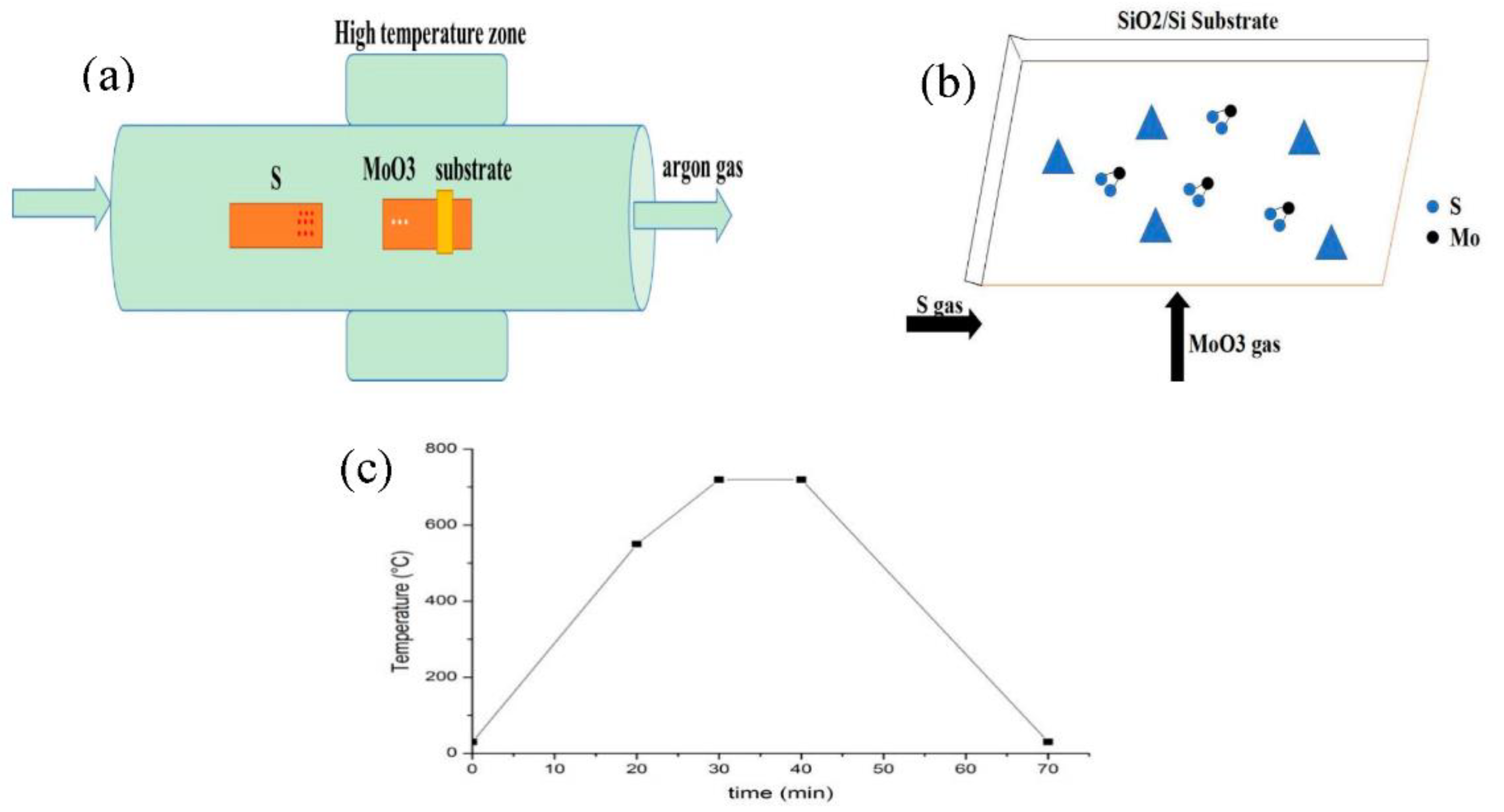
2. Experimental Methods

The specific experiment steps are provided here. First, the 4-inch silicon wafer with a thickness of 285 nm SiO2 was cut into square small pieces with an area of 4–6 cm2 by a diamond pen. Then, the SiO2/Si substrates were placed into acetone, deionized water, absolute ethanol, and deionized water for ultrasonic cleaning in 15 min, 10 min, 15 min, and 10 min, respectively [22]. And these cleaned substrates were blown dry with the nitrogen gas gun. Subsequently, a certain mass of sulfur powder (purity, 99.5%, Alfa Aesar, Shanghai, China) and MoO3 powder (purity, 99.95%, Alfa Aesar, Shanghai, China) were weighed by the electronic analytical balance, and then put into two quartz boats, respectively. Next, the first quartz boat with S powder was placed in the low temperature zone of the tube furnace, and then the second quartz boat with MoO3 powder and SiO2/Si substrate was placed in the middle position of the tube furnace, wherein the cleaned SiO2/Si substrate was placed face down on the downstream from the MoO3 powder for 5 cm, as shown in Figure 1a. Afterwards, the argon gas (purity, 99.999%) was inserted into the tube furnace in order to purge the air in the tube furnace, a flow rate of 300 sccm (1 sccm = 1 mL/min) argon gas was then introduced in the tube furnace for 5 min before the heating process. Figure 1b shows the growth mechanism of MoS2. During the heating process, argon gas with a flow rate of 35 sccm was continuously supplied as the carrier gas. It can be observed from Figure 1c that the temperature of the SiO2/Si substrate rises from room temperature to 550 °C in 20 min initially, then rises to 720 °C in 10 min, and maintains the growth temperature 720 °C in 10 min, and then cools to room temperature naturally. Finally, the samples were taken out and some characterizations on the grown MoS2 samples were executed.
To characterize the surface morphology of grown MoS2, the new generation of high-resolution Raman spectrometer LabRam HR Evolution produced by HORIBA Jobin Yvon, was used. First, the MoS2 sample was placed on the stage of the microscope, then the Hg lamp emit laser light to the MoS2 sample. Subsequently, the scattered light from the monolayer MoS2 was collected and removed by the coupled optical path and the Rayleigh filter, respectively. Finally, the light was be converted into electrical signal by the charge coupled device (CCD), which is a special semiconductor device with many photosensitive elements in the LabRam HR Evolution with the single grating. The specific test conditions were: Spectral range of 300–450 cm−1; PL of 600–800 nm; spectral resolution ≤ 0.65 cm−1; spatial resolution was Lateral ≤ 1 μm, longitudinal ≤ 2 μm; Raman spectrum of 10 mW; PL spectrum of 25 mW; the scan time of 10 s; and the accumulation time of 3 s. The Raman and photoluminescence characterization were measured by using the LabRam HR Evolution with 532 nm laser and 50 × objective [23,24,25]. At the same time, in order to master the growth mechanism of monolayer MoS2, the X-ray photoelectron spectroscopy and Atomic Force Microscope, were also used.

3. The Experimental Results and Discussion

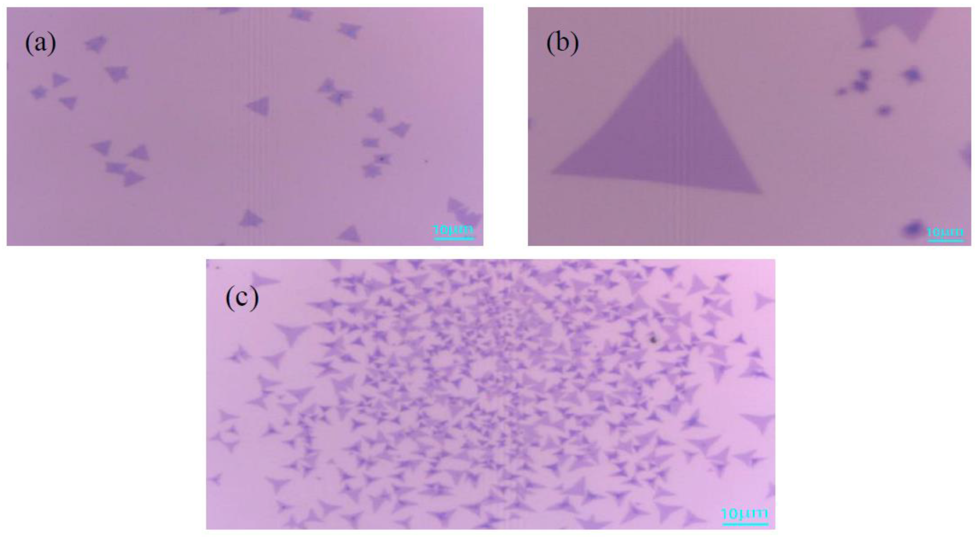
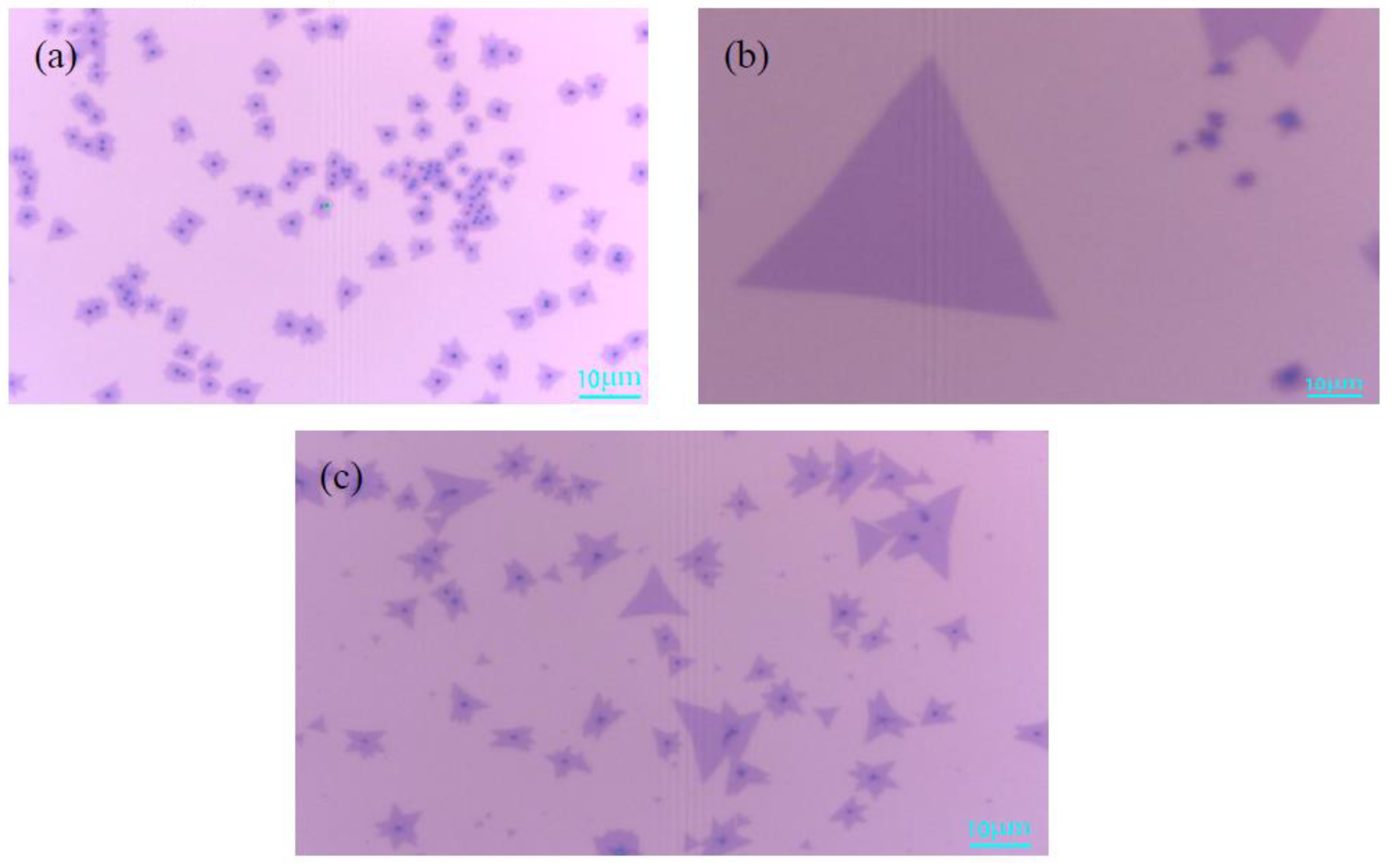
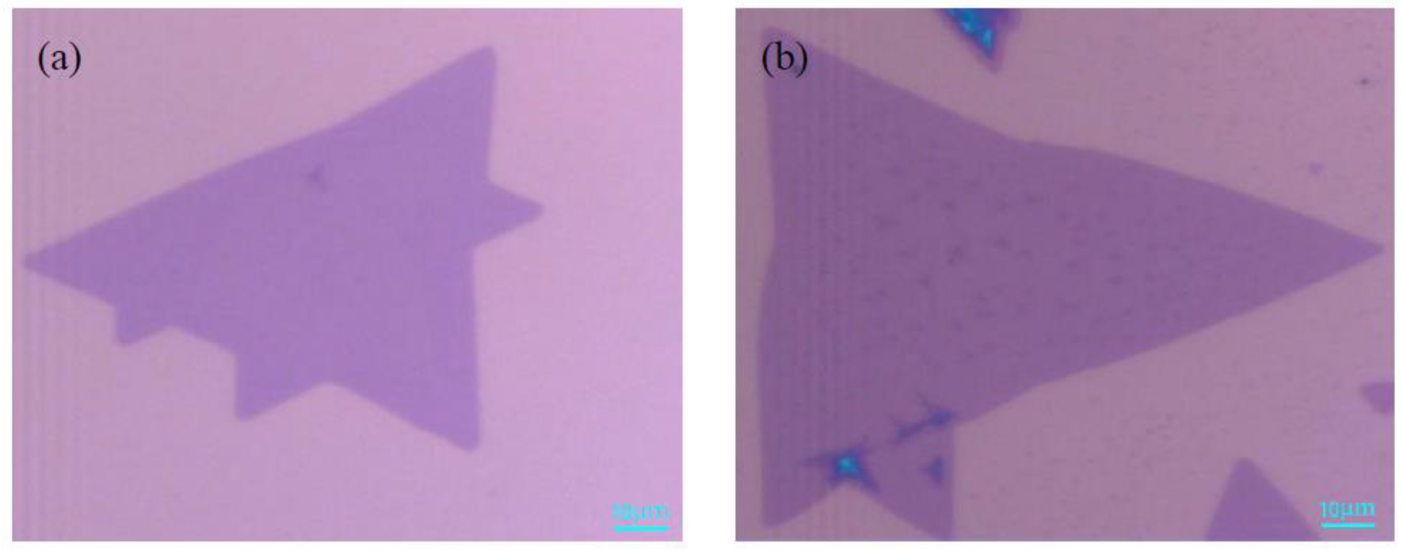
3.1. Effects of the Growth Temperature on MoS2

Figure 2a is an optical micrograph of MoS2 grown at 670 °C. A small amount of triangular monolayer MoS2 on the substrate, 8–10 μm in size, was observed. The temperature was lower, the MoO3 powder evaporated slowly, and most of the MoO3 was carried away by the argon gas, which resulted in a small amount of MoS2 deposit on the substrate. Figure 2b shows a very regular triangular MoS2, and that the single crystal size can reach up to 40 μm, which indicates that the gas concentration of MoS2 is sufficient and the nucleation density of MoS2 increases when the growth temperature is 720 °C. In Figure 2c, the substrate exists as both triangular MoS2 and some body materials, which is due to the temperature being too high and the MoO3 powder evaporating quickly, thereby forming a mixture of MoO3 and MoS2. The above analysis indicates that 720 °C is the ideal temperature for growth of the monolayer MoS2.

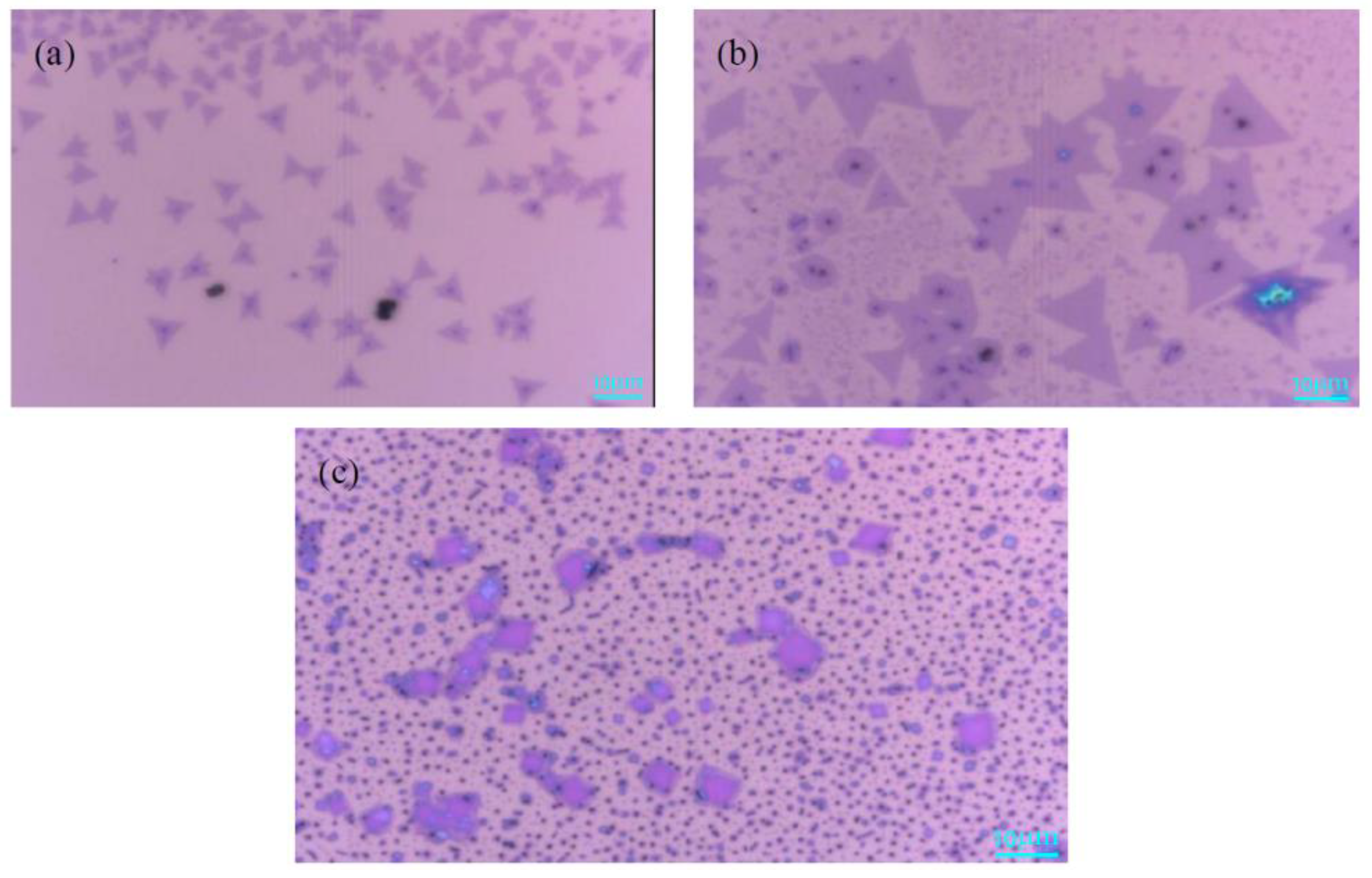
3.2. Effects of the Mass of MoO3 Powder on MoS2

The mass of MoO3 has a direct impact on the growth of MoS2 crystals. Under the premise that other growth conditions are consistent, 1 mg, 3 mg, and 5 mg of the MoO3 powder were weighed during the experiment, respectively. Figure 3a is an optical microscope image of MoS2 when the mass of MoO3 is 1 mg. It can be found that the size of the triangular single crystal MoS2 is about 10 μm, the surface of the sample is clean, and the contrast between the sample and the substrate is obvious. This is because the amount of MoO3 was small, which lead to low nucleation density. Figure 3b shows that the size of single crystal MoS2 can be as large as 30 μm, and the morphology of the sample was better, which reveals that the Mo:S ratio is >1:2 and the gas concentration of MoS2 is sufficient in this area. Meanwhile, the nucleation density is high. In Figure 3c, there is no obvious triangular single crystal MoS2, and the surface of SiO2/Si substrate is covered with fine black particles when the amount of MoO3 is increased to 5 mg. The reason is that the excessive amount of molybdenum source, which resulted in a large nucleation density and MoS2, grew toward the bulk material. From the above comparison, it can be found that the optimum mass of MoO3 is 3 mg.

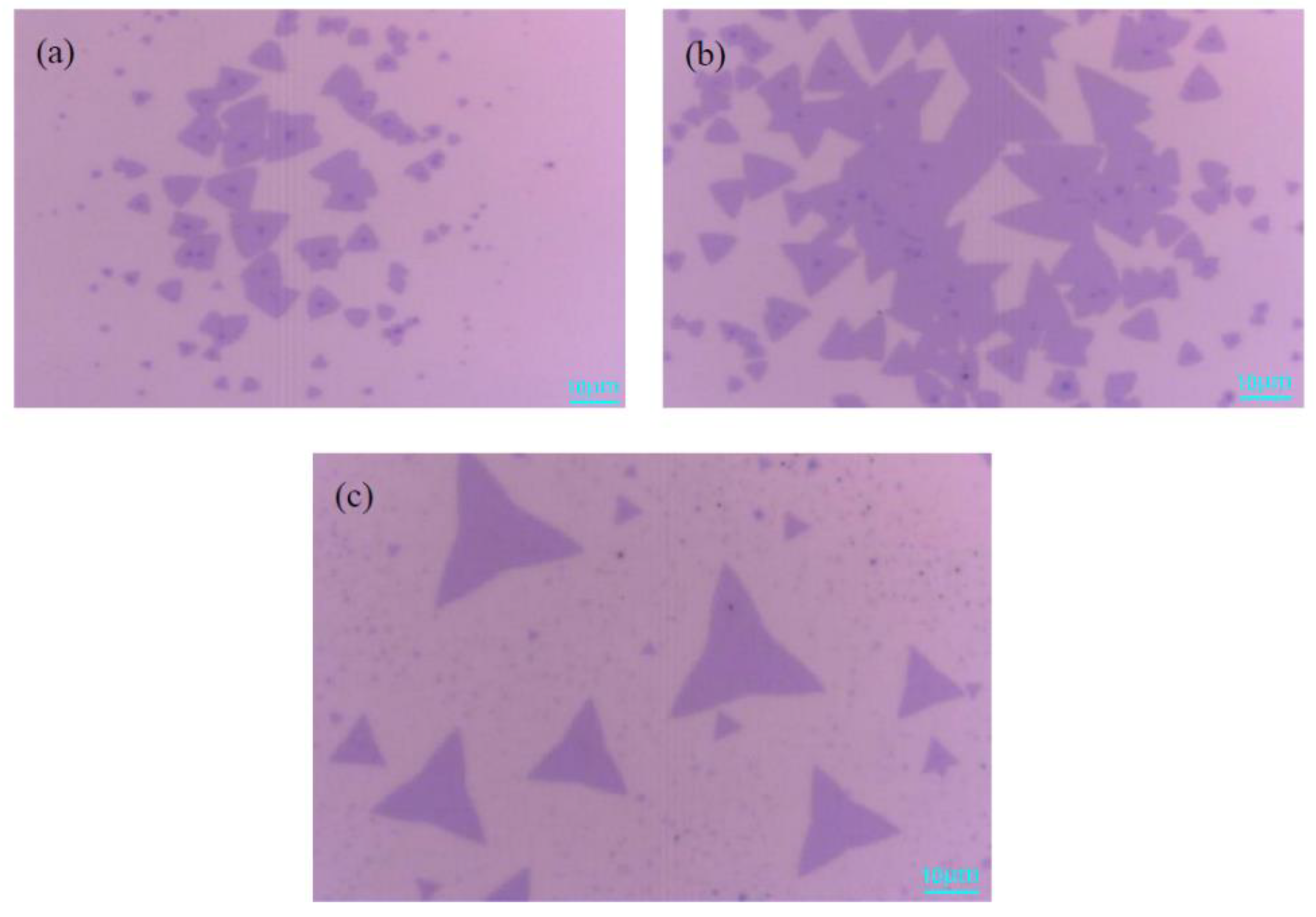
3.3. Effects of the Mass of S Powder on MoS2

In Figure 4a, when the mass of S powder was 50 mg, some small triangles and black dots were formed on the substrate, the ratio of Mo:S was <1:2. The sulfur powder was too little to provide enough S gas to react with MoO3, which caused the MoO3 to be deposited on the substrate in the form of particles. Figure 4b shows that the shape of MoS2 is very regular, and the size of MoS2 can reach up to 40 μm, which reveals that the nucleation density is high and the gas concentration of MoS2 is sufficient in this area. Meanwhile, when the Mo:S ratio was >1:2, it increased the size of MoS2. When the mass of sulfur powder was increased to 150 mg, the shape of MoS2 in Figure 4c was the same as that in Figure 4b. When the Mo:S ratio was >1:2, it produced lager triangles. It can be inferred that the mass of S powder should be excessive during the experiment, which is beneficial to the growth of monolayer MoS2. The optimum mass of S powder is 100 mg according to the above results.

3.4. Effects of the Argon Flow Rate on MoS2

The high purity argon gas had two functions during the experiment. The first was to prevent impure gas from entering the tube furnace so that the reaction of sulfurized molybdenum trioxide would be carried out in the argon gas. The second was to transport S gas to the high temperature zone to react with the MoO3 gas. Finally, the MoS2 was transferred on the surface of substrate.
Figure 5a shows a mixture of MoO2 and MoS2 on the substrate. Owing to the sufficient S, gas could not be transported to the top of the MoO3, and the synthesis efficiency of MoS2 gas was relatively low, which limited the growth response of MoS2 when the argon flow rate is 20 sccm. In Figure 5b, it is observed that the shape of the MoS2 is triangular, and the MoS2 single crystal has a size of 60 μm when the argon gas flow rate is 35 sccm. The suitable argon flow rate caused the reaction of sulfurized molybdenum trioxide more thoroughly, which can make the gas concentration of MoS2 higher. In Figure 5c, the size of the MoS2 single crystal is greatly reduced, and the number of monolayer MoS2 is also sparse. It can be inferred that the surface of SiO2/Si substrate is not conducive to the nucleation and growth of monolayer MoS2 when the gas flow is 50 sccm. When the flow rate of argon gas becomes larger, the gas concentration and the nucleation density of MoS2 become smaller, resulting in the size of the triangular MoS2 becomes smaller. In summary, the optimal argon flow rate is 35 sccm.
According to the above analysis, the optimal growth conditions for monolayer MoS2 were obtained by atmospheric pressure chemical vapor deposition. The optimal growth parameters were: 720 °C temperature, 3 mg MoO3 powder, 100 mg S powder, and 35 sccm argon gas. At the same time, the Atomic Force Microscope, Raman spectroscopic, and X-ray photoelectron spectrum were used to analyze the prepared monolayer MoS2 sample under optimal growth conditions.

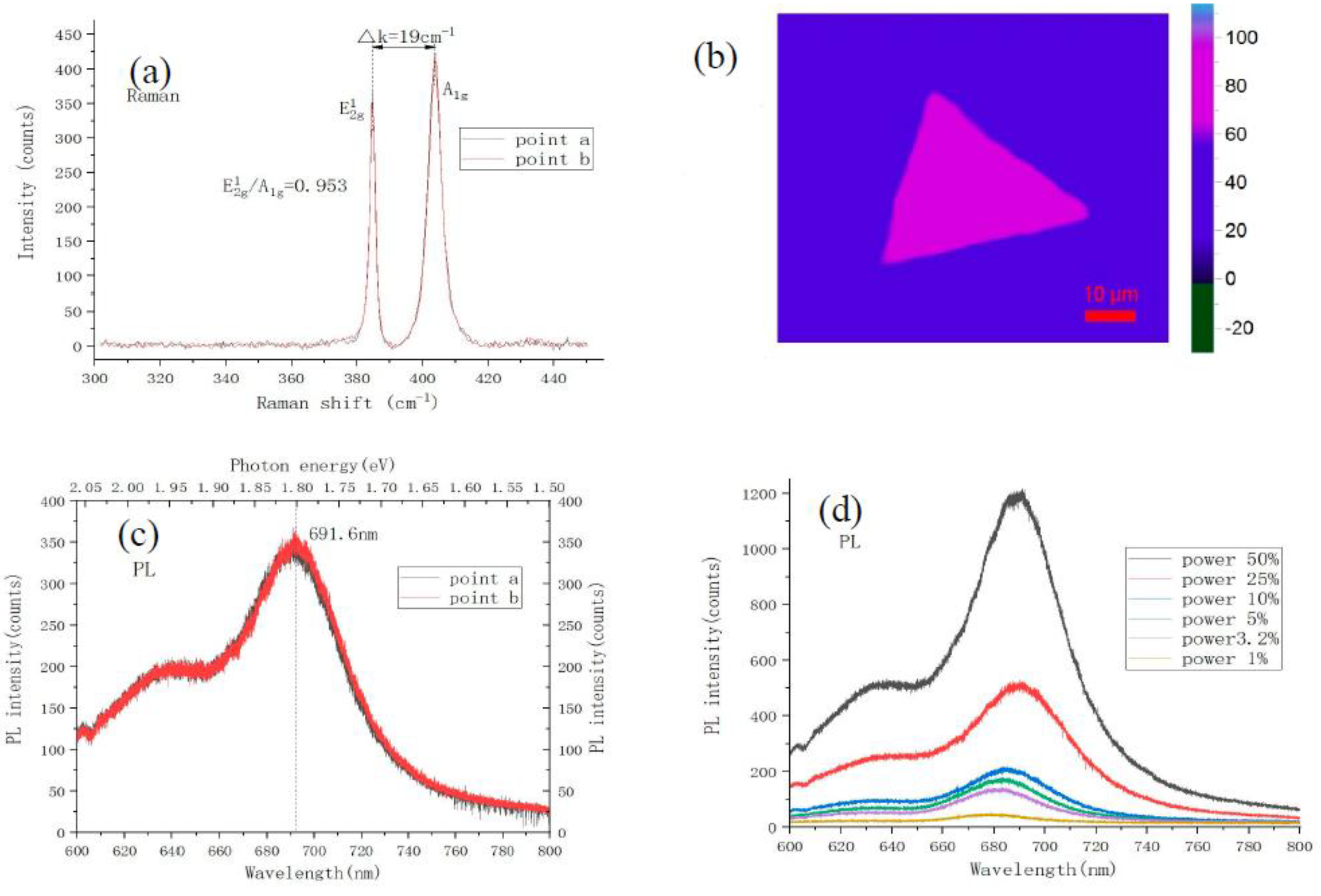
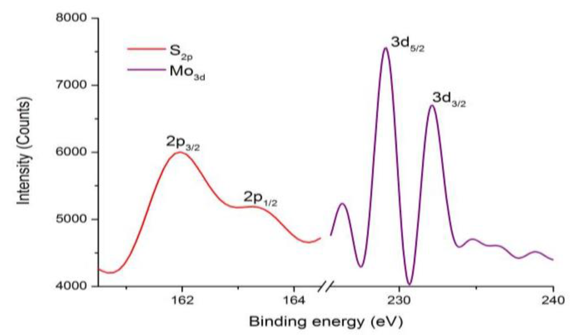
4. The Characterization of Monolayer MoS2 under Optimal Growth Conditions

In Figure 6, it is observed that the grown MoS2 is a triangle with a size of 100 μm, which is much larger than the peeled off sample micromechanically. When the growth of MoS2 is under optimal growth conditions, the gas concentration of MoS2 is the largest and the nucleation density reaches a maximum. Moreover, the surface of the grown MoS2 is uniform, and the contrast between the sample and SiO2/Si substrate is obvious. Therefore, the grown MoS2 by optimal conditions can be judged to be a single-layer initially.
Raman spectrum has become an effective method for the detection and identification of films prepared by chemical vapor deposition (CVD). The optical properties of monolayer MoS2, obtained under optimal growth conditions, are characterized by Raman and PL spectroscopies. These spectral measurement conditions were in a super-clean lab with constant temperature and humidity. Figure 7a shows two obvious characteristic peaks in the Raman spectrum of MoS2, E12g: 384.6 cm−1, A1g: 403.6 cm−1, which is fitted by the Gaussian-Lorenze curve. The E12g peak corresponds to the vibration of sulfur atoms in the horizontal plane, and A1g peak represents the vibration of sulfur atoms in the vertical horizontal plane direction. Due to the gradual increase of the van der Waals force, the E12g characteristic peak was blue-shifted, and the A1g characteristic peak was red-shifted when the number of layers was reduced [26]. Therefore, the layer number of MoS2 sample can be determined based on the wavenumber difference of two characteristic peaks A1g and E12g modes. It can be seen from the above two peak positions in Figure 7a that the wavenumber difference is about 19 cm−1, and the intensity ratio of E12g/A1g ≈ 0.95, which indicates that the grown MoS2 sample is a monolayer. Figure 7b is a triangular MoS2 single crystal with Raman mapping image of the A1g peak intensity (4000 points total), which is randomly selected on the grown MoS2 sample. It can be seen from Figure 7b that the thickness of triangular MoS2 is uniformly high. To the best of our knowledge, when MoS2 transforms from bulk material into monolayer material, the band gap changes from indirect band gap to direct band gap, and the fluorescence efficiency is enhanced significantly. Figure 7c shows the PL spectrum fitted by the Gaussian-Lorenze curve, the two main exciton peaks of the monolayer MoS2 luminescence are located at 642 nm (B excitons) and 691 nm (A excitons), respectively. The neutral excitons of A and B arise from valence band to conduction band transitions within the direct band gap of monolayer MoS2, directly. The relative contribution of excitons and triangles determines the peak position of PL spectrum. The shape of PL spectrum is consistent with the previous reported result of monolayer MoS2 obtained by mechanically exfoliated, CVD, physical vapor deposition (PVD), and so on [27,28,29]. Due to strain during thermal growth and different test environments, the peak position of A and B exciton results in a small fluctuation shift, which is within the allowable range [30]. According to the conversion relationship between wavelength and electron volt, the photon energy is inversely proportional to the wavelength:
E = h × H = h k × C λ = 1243 λ
In the formula (1), the symbol E, h, C, λ and k refer to the energy, Planck constant, light speed, wavelength and constant, respectively. Their units respectively are eV, J·s, nm/s, nm and J/eV.
The strongest luminescence peak is at 691.6 nm, the transition energy level is about 1.80 eV in Figure 7c. It is known that the direct band-gap of monolayer MoS2 is 1.8–1.9 eV, which can further prove that the sample is a monolayer MoS2. Figure 7d is the power-dependent PL spectrum of monolayer MoS2 under ambient condition, it can be seen that the PL intensity increases as laser power increases, and the relative positions of the A and B neutral excitons in the PL spectrum take place red-shifting, when the laser power increases due to the n-type doping of SiO2/Si substrate.
In order to obtain the binding energy of grown MoS2, the X-ray photoelectron spectroscopy (XPS) of Theta 300 XPS system, produced by Thermo Fisher, was adopted. The specific test conditions were: Source Gun Type: Al K Alpha; Spot Size: 650 μm; Lens Mode: Standard; Analyser Mode: Pass Energy 30.0 eV of CAE; Energy Step Size: 0.100 eV; Number of Energy Steps: 181, the number of scans in S2p and Mo3d is 8 and 7, respectively. The X-ray photoelectron spectrum image of the MoS2 sample is shown in Figure 8, it can be observed that the MoS2 sample have Mo4+ and S2− signals, which is consistent with the results reported in the literature [31]. The 3d orbital peaks of Mo are at 229.17 eV and 232.17 eV, corresponding to 3d5/2 and 3d3/2 orbitals respectively. The 2p orbital peaks of S are at 161.97 eV and 163.27 eV, corresponding to 2p3/2 and 2p1/2 orbitals respectively. At the same time, the atomic percentages of Mo3d and S2p elements are 5.42% and 11.36%, respectively, which indicates that the ratio of the atomic numbers of Mo and S is approximately 1:2. It indicates the presence of monolayer MoS2.
Figure 9a shows that the surface roughness of MoS2 sample is extremely low, the contrast and height of the sample surface are not changed obviously, which indicates the formation of monolayer MoS2 [32]. The height of the MoS2 sample in Figure 9b is around 0.72 nm. Therefore, it further evidences that the grown MoS2 is a single layer.

5. Conclusions

The large-size and high-quality monolayer MoS2 is grown on the Si substrate with a 285-nm-thick oxide layer by APCVD. The effects of MoO3 powder, S powder, temperature and argon flow rate on the growth of MoS2 are analyzed systematically. The optimum growth condition parameters for monolayer MoS2 are: 720 °C temperature, 3 mg MoO3 powder, 100 mg S powder and 35 sccm argon gas. The above results can effectively help us to understand the morphology and optical properties of monolayer MoS2. The optical microscopy, XPS, AFM, Raman, and photoluminescence spectroscopy are used to characterize the grown monolayer MoS2 under optimal condition. The results show that the grown MoS2 sample is a single layer with the size of 100μm, which can pave the way for the applications of photodetectors and transistors.

Author Contributions

Conceptualization, H.L. and T.H.; methodology, S.W.; software, S.C.; validation, T.H., W.L. and M.C.; data curation, X.Y.; writing—original draft preparation, T.H.; writing—review and editing, H.L. and W.L.; funding acquisition, H.L.

Funding

This research was funded by the National Natural Science Foundation of China (Grant No. 61434007 and Grant No. U1866212), the Foundation for Fundamental Research of China (Grant No. JSZL2016110B003), the Major Fundamental Research Program of Shaanxi (Grant 2017ZDJC-26), and supported by 111 project (Grant No. B12026).

Conflicts of Interest

The authors declare no conflict of interest.

References

  1. Lopez-Sanchez, O.; Alarcon Llado, E.; Koman, V.; Fontcuberta i Morral, A.; Radenovic, A.; Kis, A. Light generation and harvesting in a van der Waals heterostructure. ACS Nano 2014, 8, 3042–3048. [Google Scholar] [CrossRef] [PubMed]
  2. Lopez-Sanchez, O.; Lembke, D.; Kayci, M.; Radenovic, A.; Kis, A. Ultrasensitive photodetectors based on monolayer MoS2. Nat. Nanotechnol. 2013, 8, 497. [Google Scholar] [CrossRef] [PubMed]
  3. Yin, Z.; Li, H.; Li, H.; Jiang, L.; Shi, Y.; Sun, Y.; Lu, G.; Zhang, Q.; Chen, X.; Zhang, H. Single-layer MoS2 phototransistors. ACS Nano 2011, 6, 74–80. [Google Scholar] [CrossRef] [PubMed]
  4. Sundaram, R.; Engel, M.; Lombardo, A.; Krupke, R.; Ferrari, A.; Avouris, P.; Steiner, M. Electroluminescence in single layer MoS2. Nano Lett. 2013, 13, 1416–1421. [Google Scholar] [CrossRef] [PubMed]
  5. Hinnemann, B.; Moses, P.G.; Bonde, J.; Jørgensen, K.P.; Nielsen, J.H.; Horch, S.; Chorkendorff, I.; Nørskov, J.K. Biomimetic hydrogen evolution: MoS2 nanoparticles as catalyst for hydrogen evolution. J. Am. Chem. Soc. 2005, 127, 5308–5309. [Google Scholar] [CrossRef] [PubMed]
  6. Lauritsen, J.V.; Kibsgaard, J.; Helveg, S.; Topsøe, H.; Clausen, B.S.; Lægsgaard, E.; Besenbacher, F. Size-dependent structure of MoS2 nanocrystals. Nat. Nanotechnol. 2007, 2, 53. [Google Scholar] [CrossRef] [PubMed]
  7. Das, S.; Chen, H.-Y.; Penumatcha, A.V.; Appenzeller, J. High performance multilayer MoS2 transistors with scandium contacts. Nano Lett. 2012, 13, 100–105. [Google Scholar] [CrossRef]
  8. Lee, G.-H.; Yu, Y.-J.; Cui, X.; Petrone, N.; Lee, C.-H.; Choi, M.S.; Lee, D.-Y.; Lee, C.; Yoo, W.J.; Watanabe, K. Flexible and transparent MoS2 field-effect transistors on hexagonal boron nitride-graphene heterostructures. ACS Nano 2013, 7, 7931–7936. [Google Scholar] [CrossRef]
  9. Liu, H.; Neal, A.T.; Ye, P.D. Channel length scaling of MoS2 MOSFETs. ACS Nano 2012, 6, 8563–8569. [Google Scholar] [CrossRef]
  10. Bertolazzi, S.; Krasnozhon, D.; Kis, A. Nonvolatile memory cells based on MoS2/graphene heterostructures. ACS Nano 2013, 7, 3246–3252. [Google Scholar] [CrossRef]
  11. Kaasbjerg, K.; Thygesen, K.S.; Jacobsen, K.W. Phonon-limited mobility in n-type single-layer MoS2 from first principles. Phys. Rev. B 2012, 85, 115317. [Google Scholar] [CrossRef]
  12. Zhang, Y.; Oka, T.; Suzuki, R.; Ye, J.; Iwasa, Y. Electrically switchable chiral light-emitting transistor. Science 2014, 344, 725–728. [Google Scholar] [CrossRef] [PubMed]
  13. He, Q.; Zeng, Z.; Yin, Z.; Li, H.; Wu, S.; Huang, X.; Zhang, H. Fabrication of flexible MoS2 thin-film transistor arrays for practical gas-sensing applications. Small 2012, 8, 2994–2999. [Google Scholar] [CrossRef] [PubMed]
  14. Li, H.; Yin, Z.; He, Q.; Li, H.; Huang, X.; Lu, G.; Fam, D.W.H.; Tok, A.I.Y.; Zhang, Q.; Zhang, H. Fabrication of single-and multilayer MoS2 film-based field-effect transistors for sensing NO at room temperature. Small 2012, 8, 63–67. [Google Scholar] [CrossRef] [PubMed]
  15. Chae, W.H.; Cain, J.D.; Hanson, E.D.; Murthy, A.A.; Dravid, V.P. Substrate-induced strain and charge doping in CVD-grown monolayer MoS2. Appl. Phys. Lett. 2017, 111, 143106. [Google Scholar] [CrossRef]
  16. Li, X.; Zhu, H. Two-dimensional MoS2: Properties, preparation, and applications. J. Materiom. 2015, 1, 33–44. [Google Scholar] [CrossRef]
  17. Zafar, A.; Nan, H.; Zafar, Z.; Wu, Z.; Jiang, J.; You, Y.; Ni, Z. Probing the intrinsic optical quality of CVD grown MoS2. Nano Res. 2017, 10, 1608–1617. [Google Scholar] [CrossRef]
  18. Novoselov, K.; Jiang, D.; Schedin, F.; Booth, T.; Khotkevich, V.; Morozov, S.; Geim, A. Two-dimensional atomic crystals. Proc. Nat. Acad. Sci. USA 2005, 102, 10451–10453. [Google Scholar] [CrossRef] [Green Version]
  19. Jiang, L.; Lin, B.; Li, X.; Song, X.; Xia, H.; Li, L.; Zeng, H. Monolayer MoS2–graphene hybrid aerogels with controllable porosity for lithium-ion batteries with high reversible capacity. ACS Appl. Mater. Inter. 2016, 8, 2680–2687. [Google Scholar] [CrossRef]
  20. Wu, J.; Dai, J.; Shao, Y.; Cao, M.; Wu, X. Carbon dot-assisted hydrothermal synthesis of flower-like MoS2 nanospheres constructed by few-layered multiphase MoS2 nanosheets for supercapacitors. RSC Adv. 2016, 6, 77999–78007. [Google Scholar] [CrossRef]
  21. Chow, P.K.; Singh, E.; Viana, B.C.; Gao, J.; Luo, J.; Li, J.; Lin, Z.; Elías, A.L.; Shi, Y.; Wang, Z. Wetting of mono and few-layered WS2 and MoS2 films supported on Si/SiO2 substrates. ACS Nano 2015, 9, 3023–3031. [Google Scholar] [CrossRef] [PubMed]
  22. Wen, Y.-N.; Xia, M.-G.; Zhang, S.-L. Size effect on the magnetic and electronic properties of the monolayer lateral hetero-junction WS2-MoS2 nanoribbon. Appl. Surf. Sci. 2016, 371, 376–382. [Google Scholar] [CrossRef]
  23. Friedman, A.L.; Perkins, F.K.; Cobas, E.; Jernigan, G.G.; Campbell, P.M.; Hanbicki, A.T.; Jonker, B.T. Chemical vapor sensing of two-dimensional MoS2 field effect transistor devices. Solid-State Electron. 2014, 101, 2–7. [Google Scholar] [CrossRef]
  24. Late, D.J.; Huang, Y.-K.; Liu, B.; Acharya, J.; Shirodkar, S.N.; Luo, J.; Yan, A.; Charles, D.; Waghmare, U.V.; Dravid, V.P. Sensing behavior of atomically thin-layered MoS2 transistors. ACS Nano 2013, 7, 4879–4891. [Google Scholar] [CrossRef] [PubMed]
  25. Qiu, D.; Lee, D.U.; Pak, S.W.; Kim, E.K. Structural and optical properties of MoS2 layers grown by successive two-step chemical vapor deposition method. Thin Solid Films 2015, 587, 47–51. [Google Scholar] [CrossRef]
  26. Li, Z.; Ye, R.; Feng, R.; Kang, Y.; Zhu, X.; Tour, J.M.; Fang, Z. Graphene quantum dots doping of MoS2 monolayers. Adv. Mater. 2015, 27, 5235–5240. [Google Scholar] [CrossRef] [PubMed]
  27. Frisenda, R.; Niu, Y.; Gant, P.; Molina-Mendoza, A.J.; Schmidt, R.; Bratschitsch, R.; Liu, J.; Fu, L.; Dumcenco, D.; Kis, A. Micro-reflectance and transmittance spectroscopy: A versatile and powerful tool to characterize 2D materials. J. Phys. D Appl. Phys. 2017, 50, 074002. [Google Scholar] [CrossRef]
  28. Xu, H.; Zhou, W.; Zheng, X.; Huang, J.; Feng, X.; Ye, L.; Xu, G.; Lin, F. Control of the Nucleation Density of Molybdenum Disulfide in Large-Scale Synthesis Using Chemical Vapor Deposition. Materials 2018, 11, 870. [Google Scholar] [CrossRef]
  29. Xu, W.; Li, S.; Zhou, S.; Lee, J.K.; Wang, S.; Sarwat, S.G.; Wang, X.; Bhaskaran, H.; Pasta, M.; Warner, J.H. Large Dendritic Monolayer MoS2 Grown by Atmospheric Pressure Chemical Vapor Deposition for Electrocatalysis. ACS Appl. Mater. Interfaces 2018, 10, 4630–4639. [Google Scholar] [CrossRef]
  30. Plechinger, G.; Mann, J.; Preciado, E.; Barroso, D.; Nguyen, A.; Eroms, J.; Schueller, C.; Bartels, L.; Korn, T. A direct comparison of CVD-grown and exfoliated MoS2 using optical spectroscopy. Semicond. Sci. Technol. 2014, 29, 064008. [Google Scholar] [CrossRef]
  31. Wang, S.; Rong, Y.; Fan, Y.; Pacios, M.; Bhaskaran, H.; He, K.; Warner, J.H. Shape evolution of monolayer MoS2 crystals grown by chemical vapor deposition. Chem. Mater. 2014, 26, 6371–6379. [Google Scholar] [CrossRef]
  32. Li, X.; Li, X.; Zang, X.; Zhu, M.; He, Y.; Wang, K.; Xie, D.; Zhu, H. Role of hydrogen in the chemical vapor deposition growth of MoS2 atomic layers. Nanoscale 2015, 7, 8398–8404. [Google Scholar] [CrossRef] [PubMed]
Figure 1. (a) Schematic illustration of the single temperature zone chemical vapor deposition (CVD) system; (b) schematic diagram of the MoS2 growth; (c) temperature change curve diagram of the SiO2/Si substrate.
Materials 11 02562 g001
Figure 2. Optical microscope images of MoS2 grown at different temperatures (a) 670 °C; (b) 720 °C; (c) 770 °C. Scale bar: 10 μm.
Materials 11 02562 g002
Figure 3. Optical microscope images of MoS2 with the different MoO3 mass (a) 1 mg; (b) 3 mg; (c) 5 mg. Scale bar: 10 μm.
Materials 11 02562 g003
Figure 4. Optical microscope images of MoS2 with the different mass of S powder (a) 50 mg; (b) 100 mg; (c) 150 mg. Scale bar: 10 μm.
Materials 11 02562 g004
Figure 5. Optical microscope images of MoS2 with different argon flow rate (a) 20 sccm; (b) 35 sccm; (c) 50 sccm. Scale bar: 10 μm.
Materials 11 02562 g005
Figure 6. Optical microscope images of two different positions of the same sample (a) 80 μm; (b) 100 μm. Scale bar: 10 μm.
Materials 11 02562 g006
Figure 7. Raman and photoluminescence spectrum of the monolayer MoS2. (a) is the Raman spectrum of MoS2 corresponding to Figure 6, wherein the black line corresponds to Figure 6a, and the red line corresponds to Figure 6b; (b) is the Raman mapping of A1g; (c) shows the MoS2 photoluminescence spectrum corresponding to Figure 6. The black line corresponds to Figure 6a, and the red line corresponds to Figure 6b; (d) is the power-dependant PL spectrum under ambient condition.
Materials 11 02562 g007
Figure 8. XPS spectra of Mo3d and S2p for the monolayer MoS2.
Materials 11 02562 g008
Figure 9. (a) Two-dimensional AFM topography image of the monolayer MoS2; (b) Height profile of the monolayer MoS2.
Materials 11 02562 g009

