Plasmonic Metasurface Absorber Based on Electro-Optic Substrate for Energy Harvesting

 and
and 
Abstract
1. Introduction
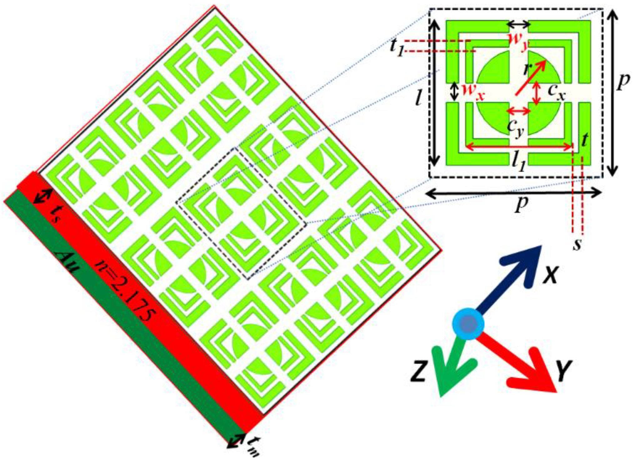
2. Physical Design
3. Results and Discussion
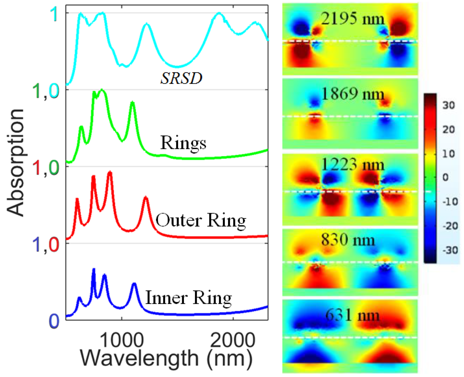
3.1. Basic Studies
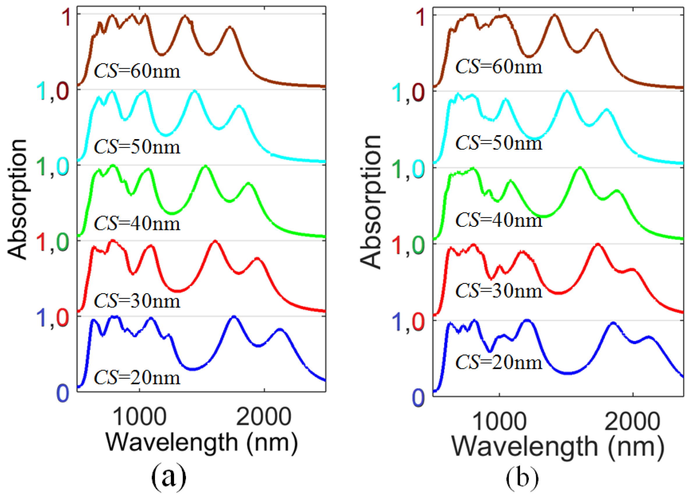
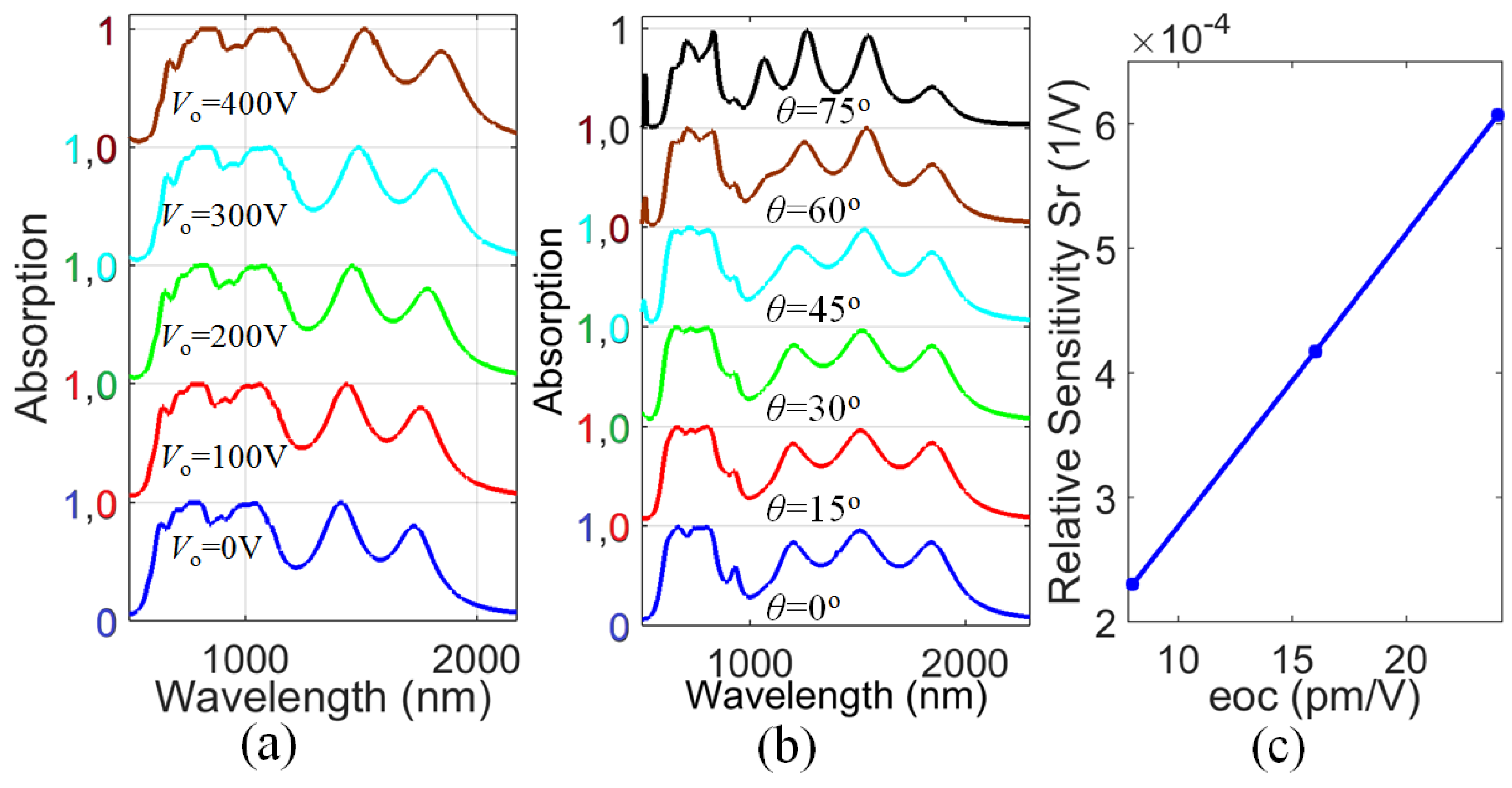
3.2. Influence of Structural Parameters on the Absorption Spectra
4. Conclusion
Author Contributions
Funding
Conflicts of Interest
References
- Shelby, R.A.; Smith, D.R.; Schultz, S. Experimental verification of a negative index of refraction. Science 2001, 292, 77–79. [Google Scholar] [CrossRef] [PubMed]
- Ramakrishna, S.A. Physics of negative refractive index materials. Rep. Prog. Phys. 2005, 68, 449. [Google Scholar] [CrossRef]
- La Spada, L.; Vegni, L. Near-zero-index wires. Opt. Express 2017, 25, 23699–23708. [Google Scholar] [CrossRef] [PubMed]
- Fang, N.; Lee, H.; Sun, C.; Zhang, X. Sub–diffraction-limited optical imaging with a silver superlens. Science 2005, 308, 534–537. [Google Scholar] [CrossRef] [PubMed]
- Muhammad, N.; Khan, A.D. Tunable fano resonances and electromagnetically induced transparency in all-dielectric holey block. Plasmonics 2015, 10, 1687–1693. [Google Scholar] [CrossRef]
- Muhammad, N.; Khan, A.D. Electromagnetically induced transparency and sharp asymmetric fano line shapes in all-dielectric nanodimer. Plasmonics 2017, 12, 1399–1407. [Google Scholar] [CrossRef]
- Muhammad, N.; Khan, A.D.; Deng, Z.-L.; Khan, K.; Yadav, A.; Liu, Q.; Ouyang, Z. Plasmonic spectral splitting in ring/rod metasurface. Nanomaterials 2017, 7, 397. [Google Scholar] [CrossRef] [PubMed]
- Guo, C.F.; Sun, T.; Cao, F.; Liu, Q.; Ren, Z. Metallic nanostructures for light trapping in energy-harvesting devices. Light: Sci. Appl. 2014, 3, e161. [Google Scholar]
- Wang, Y.; Ren, Z.; Kempa, K. Metamaterial-plasmonic ultra-thin absorbers for thin film solar cells. In Proceedings of the Asia Communications and Photonics Conference, Guangzhou, China, 7–10 November 2012. [Google Scholar]
- Cui, Y.; He, Y.; Jin, Y.; Ding, F.; Yang, L.; Ye, Y.; Zhong, S.; Lin, Y.; He, S. Plasmonic and metamaterial structures as electromagnetic absorbers. Laser Photonics Rev. 2014, 8, 495–520. [Google Scholar] [CrossRef]
- Ra’Di, Y.; Simovski, C.; Tretyakov, S. Thin perfect absorbers for electromagnetic waves: Theory, design, and realizations. Phys. Rev. Appl. 2015, 3, 037001. [Google Scholar] [CrossRef]
- Yong, Z.; Zhang, S.; Gong, C.; He, S. Narrow band perfect absorber for maximum localized magnetic and electric field enhancement and sensing applications. Sci. Rep. 2016, 6, 24063. [Google Scholar] [CrossRef] [PubMed]
- Luo, S.; Zhao, J.; Zuo, D.; Wang, X. Perfect narrow band absorber for sensing applications. Opt. Express 2016, 24, 9288–9294. [Google Scholar] [CrossRef] [PubMed]
- Iovine, R.; La Spada, L.; Vegni, L. Nanoplasmonic sensor for chemical measurements. In Proceedings of the Optical Sensors 2013, Prague, Czech Republic, 15–18 April 2013. [Google Scholar]
- Lee, Y.; Kim, S.-J.; Park, H.; Lee, B. Metamaterials and metasurfaces for sensor applications. Sensors 2017, 17, 1726. [Google Scholar] [CrossRef] [PubMed]
- Bibbò, L.; Khan, K.; Liu, Q.; Lin, M.; Wang, Q.; Ouyang, Z. Tunable narrowband antireflection optical filter with a metasurface. Photonics Research 2017, 5, 500–506. [Google Scholar] [CrossRef]
- Landy, N.I.; Sajuyigbe, S.; Mock, J.; Smith, D.; Padilla, W. Perfect metamaterial absorber. Phys. Rev. Lett. 2008, 100, 207402. [Google Scholar] [CrossRef] [PubMed]
- Aydin, K.; Ferry, V.E.; Briggs, R.M.; Atwater, H.A. Broadband polarization-independent resonant light absorption using ultrathin plasmonic super absorbers. Nat. Commun. 2011, 2, 517. [Google Scholar] [CrossRef] [PubMed]
- Hao, J.; Wang, J.; Liu, X.; Padilla, W.J.; Zhou, L.; Qiu, M. High performance optical absorber based on a plasmonic metamaterial. Appl. Phys. Lett. 2010, 96, 251104. [Google Scholar] [CrossRef]
- Tao, H.; Landy, N.I.; Bingham, C.M.; Zhang, X.; Averitt, R.D.; Padilla, W.J. A metamaterial absorber for the terahertz regime: Design, fabrication and characterization. Opt. Express 2008, 16, 7181–7188. [Google Scholar] [CrossRef] [PubMed]
- Sun, J.; Liu, L.; Dong, G.; Zhou, J. An extremely broad band metamaterial absorber based on destructive interference. Opt. Express 2011, 19, 21155–21162. [Google Scholar] [CrossRef] [PubMed]
- Li, S.; Gao, J.; Cao, X.; Zhang, Z.; Zheng, Y.; Zhang, C. Multiband and broadband polarization-insensitive perfect absorber devices based on a tunable and thin double split-ring metamaterial. Opt. Express 2015, 23, 3523–3533. [Google Scholar] [CrossRef] [PubMed]
- XU, Y.Q.; Zhou, P.H.; Zhang, H.B.; Chen, L.; Deng, L.J. A wide-angle planar metamaterial absorber based on split ring resonator coupling. J. Appl. Phys. 2011, 110, 044102. [Google Scholar]
- Shi, C.; Zang, X.; Ji, X.; Chen, L.; Cai, B.; Zhu, Y. Ultra-Broadband Terahertz Perfect Absorber Based on Multi-Frequency Destructive Interference and Grating Diffraction. Available online: https://arxiv.org/ftp/arxiv/papers/1409/1409.6103.pdf. (accessed on 15 November 2018).
- Khan, A.D.; Amin, M. Tunable salisbury screen absorber using square lattice of plasmonic nanodisk. Plasmonics 2017, 12, 257–262. [Google Scholar] [CrossRef]
- Mulla, B.; Sabah, C. Multiband metamaterial absorber design based on plasmonic resonances for solar energy harvesting. Plasmonics 2016, 11, 1313–1321. [Google Scholar] [CrossRef]
- Wang, B.-X.; Zhai, X.; Wang, G.; Huang, W.; Wang, L. Design of a four-band and polarization-insensitive terahertz metamaterial absorber. IEEE Photonics J. 2015, 7, 1–8. [Google Scholar] [CrossRef]
- Shen, X.; Cui, T.J.; Zhao, J.; Ma, H.F.; Jiang, W.X.; Li, H. Polarization-independent wide-angle triple-band metamaterial absorber. Opt. Express 2011, 19, 9401–9407. [Google Scholar] [CrossRef] [PubMed]
- Tao, H.; Bingham, C.; Pilon, D.; Fan, K.; Strikwerda, A.; Shrekenhamer, D.; Padilla, W.; Zhang, X.; Averitt, R. A dual band terahertz metamaterial absorber. J. Phys. D Appl. Phys. 2010, 43, 225102. [Google Scholar] [CrossRef]
- Ullah, H.; Khan, A.D.; Noman, M.; Rehman, A.U. Novel multi-broadband plasmonic absorber based on a metal-dielectric-metal square ring array. Plasmonics 2017, 13, 591–597. [Google Scholar] [CrossRef]
- He, X.; Yan, S.; Lu, G.; Zhang, Q.; Wu, F.; Jiang, J. An ultra-broadband polarization-independent perfect absorber for the solar spectrum. RSC Adv. 2015, 5, 61955–61959. [Google Scholar] [CrossRef]
- Nielsen, M.G.; Pors, A.; Albrektsen, O.; Bozhevolnyi, S.I. Efficient absorption of visible radiation by gap plasmon resonators. Opt. Express 2012, 20, 13311–13319. [Google Scholar] [CrossRef] [PubMed]
- Rufangura, P.; Sabah, C. Dual-band perfect metamaterial absorber for solar cell applications. Vacuum 2015, 120, 68–74. [Google Scholar] [CrossRef]
- Zhu, L.; Wang, Y.; Liu, Y.; Yue, C. Design and analysis of ultra broadband nano-absorber for solar energy harvesting. Plasmonics 2017, 1–7. [Google Scholar] [CrossRef]
- Lei, L.; Li, S.; Huang, H.; Tao, K.; Xu, P. Ultra-broadband absorber from visible to near-infrared using plasmonic metamaterial. Opt. Express 2018, 26, 5686–5693. [Google Scholar] [CrossRef] [PubMed]
- Hedayati, M.K.; Javaherirahim, M.; Mozooni, B.; Abdelaziz, R.; Tavassolizadeh, A.; Chakravadhanula, V.S.K.; Zaporojtchenko, V.; Strunkus, T.; Faupel, F.; Elbahri, M. Design of a perfect black absorber at visible frequencies using plasmonic metamaterials. Adv. Mater. 2011, 23, 5410–5414. [Google Scholar] [CrossRef] [PubMed]
- Wu, D.; Liu, C.; Liu, Y.; Yu, L.; Yu, Z.; Chen, L.; Ma, R.; Ye, H. Numerical study of an ultra-broadband near-perfect solar absorber in the visible and near-infrared region. Opt. lett. 2017, 42, 450–453. [Google Scholar] [CrossRef] [PubMed]
- Chen, J.; Guo, J.; Chen, L.-Y. Super-wideband perfect solar light absorbers using titanium and silicon dioxide thin-film cascade optical nanocavities. Opt. Mater. Express 2016, 6, 3804–3813. [Google Scholar] [CrossRef]
- Yan, M.; Dai, J.; Qiu, M. Lithography-free broadband visible light absorber based on a mono-layer of gold nanoparticles. J. Opt. 2014, 16, 025002. [Google Scholar] [CrossRef]
- Wang, Z.; Zhang, Z.M.; Quan, X.; Cheng, P. A perfect absorber design using a natural hyperbolic material for harvesting solar energy. Solar Energy 2018, 159, 329–336. [Google Scholar] [CrossRef]
- Alici, K.B.; Turhan, A.B.; Soukoulis, C.M.; Ozbay, E. Optically thin composite resonant absorber at the near-infrared band: A polarization independent and spectrally broadband configuration. Opt. Express 2011, 19, 14260–14267. [Google Scholar] [CrossRef] [PubMed]
- Wang, H.; Yang, Y.; Wang, L. Switchable wavelength-selective and diffuse metamaterial absorber/emitter with a phase transition spacer layer. Appl. Phys. Lett. 2014, 105, 071907. [Google Scholar] [CrossRef]
- Wang, H.; Wang, L. Perfect selective metamaterial solar absorbers. Opt. Express 2013, 21, A1078–A1093. [Google Scholar] [CrossRef] [PubMed]
- Mulla, B.; Sabah, C. Perfect metamaterial absorber design for solar cell applications. Waves Random Complex Media 2015, 25, 382–392. [Google Scholar] [CrossRef]
- Bağmancı, M.; Karaaslan, M.; Altıntaş, O.; Karadağ, F.; Tetik, E.; Bakır, M. Wideband metamaterial absorber based on crrs with lumped elements for microwave energy harvesting. J. Microw. Power Electromagn. Energy 2017, 52, 1–15. [Google Scholar] [CrossRef]
- Bağmancı, M.; Karaaslan, M.; Ünal, E.; Akgol, O.; Karadağ, F.; Sabah, C. Broad-band polarization-independent metamaterial absorber for solar energy harvesting applications. Phys. E Low Dimensional Syst. Nanostruct. 2017, 90, 1–6. [Google Scholar] [CrossRef]
- Bağmancı, M.; Karaaslan, M.; Ünal, E.; Akgol, O.; Sabah, C. Extremely-broad band metamaterial absorber for solar energy harvesting based on star shaped resonator. Opt. Quantum Electron. 2017, 49, 257. [Google Scholar] [CrossRef]
- Karaaslan, M.; Bağmancı, M.; Ünal, E.; Akgol, O.; Sabah, C. Microwave energy harvesting based on metamaterial absorbers with multi-layered square split rings for wireless communications. Opt. Commun. 2017, 392, 31–38. [Google Scholar] [CrossRef]
- Hokmabadi, M.P.; Wilbert, D.S.; Kung, P.; Kim, S.M. Terahertz metamaterial absorbers. Terahertz Sci. Technol. 2013, 6, 40–58. [Google Scholar]
- Duan, G.; Schalch, J.; Zhao, X.; Zhang, J.; Averitt, R.; Zhang, X. An air-spacer terahertz metamaterial perfect absorber for sensing and detection applications. In Proceedings of the 19th International Conference on Solid-State Sensors, Actuators and Microsystems (TRANSDUCERS), Kaohsiung, Taiwan, 18–22 June 2017. [Google Scholar]
- Hedayati, M.K.; Faupel, F.; Elbahri, M. Review of plasmonic nanocomposite metamaterial absorber. Materials 2014, 7, 1221–1248. [Google Scholar] [CrossRef] [PubMed]
- Lesina, A.C.; Vaccari, A.; Berini, P.; Ramunno, L. On the convergence and accuracy of the fdtd method for nanoplasmonics. Opt. Express 2015, 23, 10481–10497. [Google Scholar] [CrossRef] [PubMed]
- Chen, H.-T. Interference theory of metamaterial perfect absorbers. Opt. Express 2012, 20, 7165–7172. [Google Scholar] [CrossRef] [PubMed]
- Ullah, H.; Khan, A.D.; Ullah, A.; Ullah, I.; Noman, M. Plasmonic perfect absorber for solar cell applications. In Proceedings of the 2016 International Conference on Emerging Technologies (ICET), Islamabad, Pakistan, 18–19 October 2016. [Google Scholar]
- Huck, C.; Neubrech, F.; Vogt, J.; Toma, A.; Gerbert, D.; Katzmann, J.; Härtling, T.; Pucci, A. Surface-enhanced infrared spectroscopy using nanometer-sized gaps. ACS Nano 2014, 8, 4908–4914. [Google Scholar] [CrossRef] [PubMed]


| Parameters | Split | 20 nm | 30 nm | 40 nm | 50 nm | 60 nm |
|---|---|---|---|---|---|---|
| wx | (%) | 61.28 | 62.02 | 62.51 | 62.86 | 62.36 |
| wy | (%) | 62.06 | 61.29 | 61.70 | 61.14 | 62.04 |
| cy | (%) | 66.90 | 66.31 | 65.33 | 63.59 | 62.31 |
| Disk Radius | CS | 20 nm | 30 nm | 40 nm | 50 nm | 60 nm |
|---|---|---|---|---|---|---|
| r = 80 nm | (%) | 69.98 | 66.94 | 65.27 | 61.68 | 63.99 |
| r = 90 nm | (%) | 69.22 | 67.85 | 65.30 | 63.44 | 66.96 |
| Substrate Thickness | 70 nm | 80 nm | 90 nm | 100 nm | 110 nm | |
|---|---|---|---|---|---|---|
| AZO | (%) | 76.35 | 67.97 | 65.26 | 57.17 | 50.36 |
| ITO | (%) | 75.31 | 66.40 | 62.78 | 55.01 | 48.33 |
| SiO2 | (%) | 70.36 | 67.94 | 68.76 | 64.61 | 60.20 |
| ZnO | (%) | 72.96 | 63.93 | 60.26 | 51.62 | 46.56 |
© 2018 by the authors. Licensee MDPI, Basel, Switzerland. This article is an open access article distributed under the terms and conditions of the Creative Commons Attribution (CC BY) license (http://creativecommons.org/licenses/by/4.0/).
Share and Cite
Muhammad, N.; Fu, T.; Liu, Q.; Tang, X.; Deng, Z.-L.; Ouyang, Z. Plasmonic Metasurface Absorber Based on Electro-Optic Substrate for Energy Harvesting. Materials 2018, 11, 2315. https://doi.org/10.3390/ma11112315
Muhammad N, Fu T, Liu Q, Tang X, Deng Z-L, Ouyang Z. Plasmonic Metasurface Absorber Based on Electro-Optic Substrate for Energy Harvesting. Materials. 2018; 11(11):2315. https://doi.org/10.3390/ma11112315
Chicago/Turabian StyleMuhammad, Naseer, Tao Fu, Qiang Liu, Xiaopin Tang, Zi-Lan Deng, and Zhengbiao Ouyang. 2018. "Plasmonic Metasurface Absorber Based on Electro-Optic Substrate for Energy Harvesting" Materials 11, no. 11: 2315. https://doi.org/10.3390/ma11112315
APA StyleMuhammad, N., Fu, T., Liu, Q., Tang, X., Deng, Z.-L., & Ouyang, Z. (2018). Plasmonic Metasurface Absorber Based on Electro-Optic Substrate for Energy Harvesting. Materials, 11(11), 2315. https://doi.org/10.3390/ma11112315