
A Study of Polycrystalline Silicon Damage Features Based on Nanosecond Pulse Laser Irradiation with Different Wavelength Effects

Abstract
:1. Introduction
2. Theoretical Analysis of Thermodynamic Effects of Polycrystalline Silicon Irradiated by Single Pulse Laser
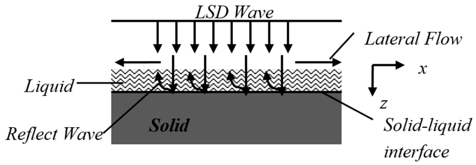
2.1. Analysis of Vapor Pressure Effect
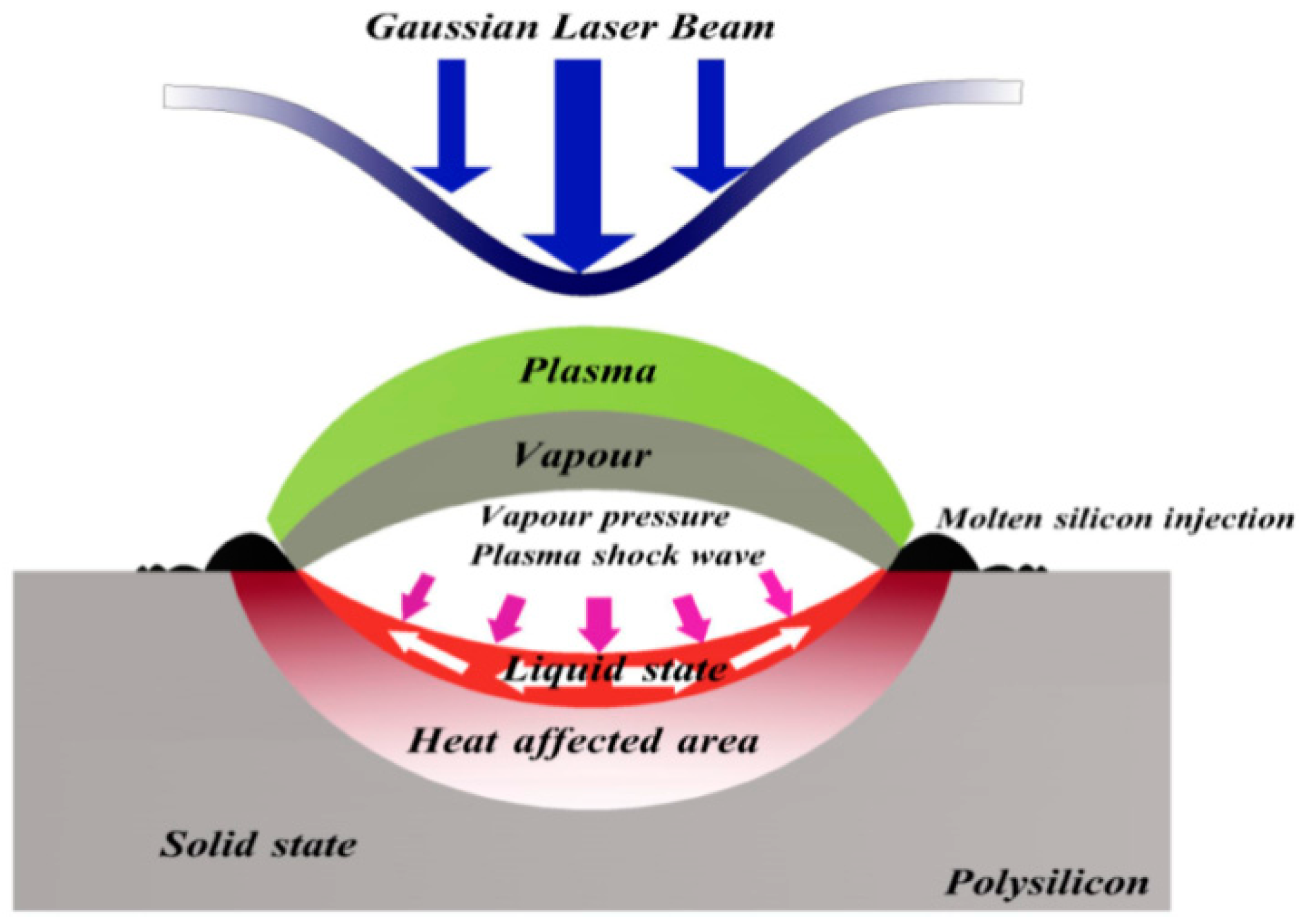
2.2. Plasma Shock Wave Pressure Effect
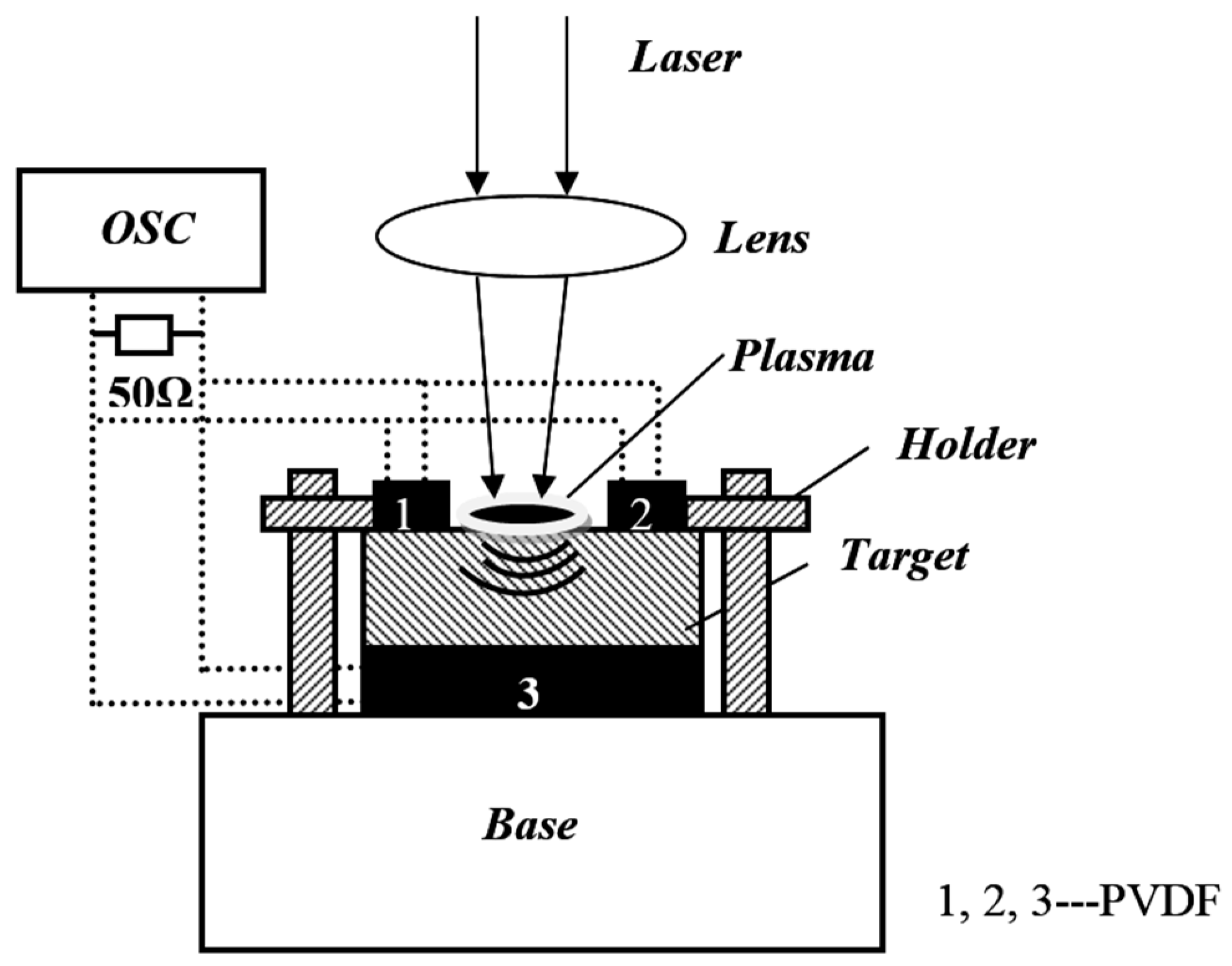
3. Experimental Equipment and Methods
4. Experimental Results and Analysis
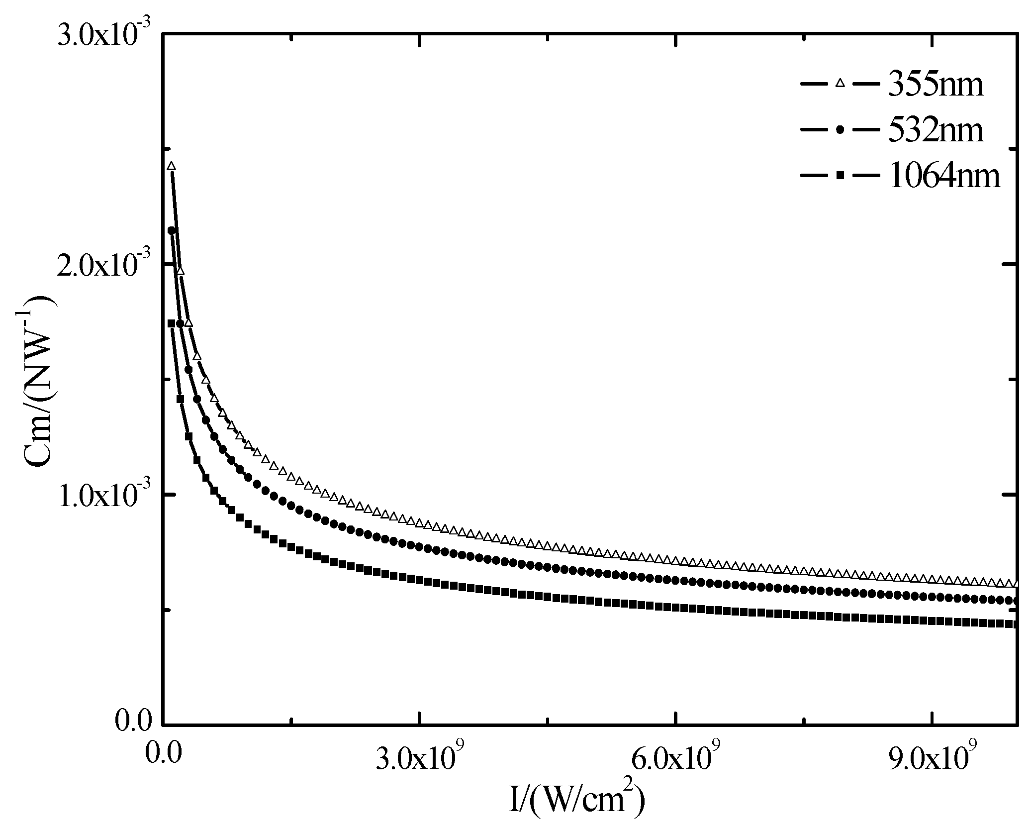
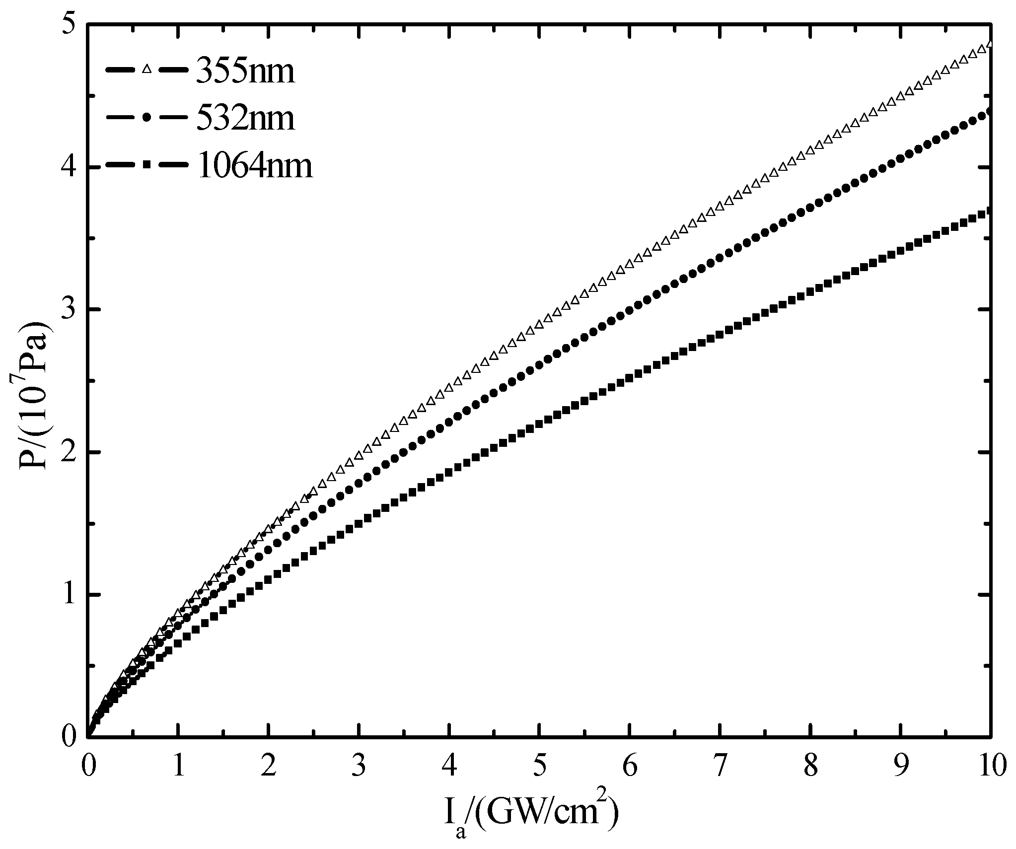
4.1. Vapor Pressure Effect on the Target Surface
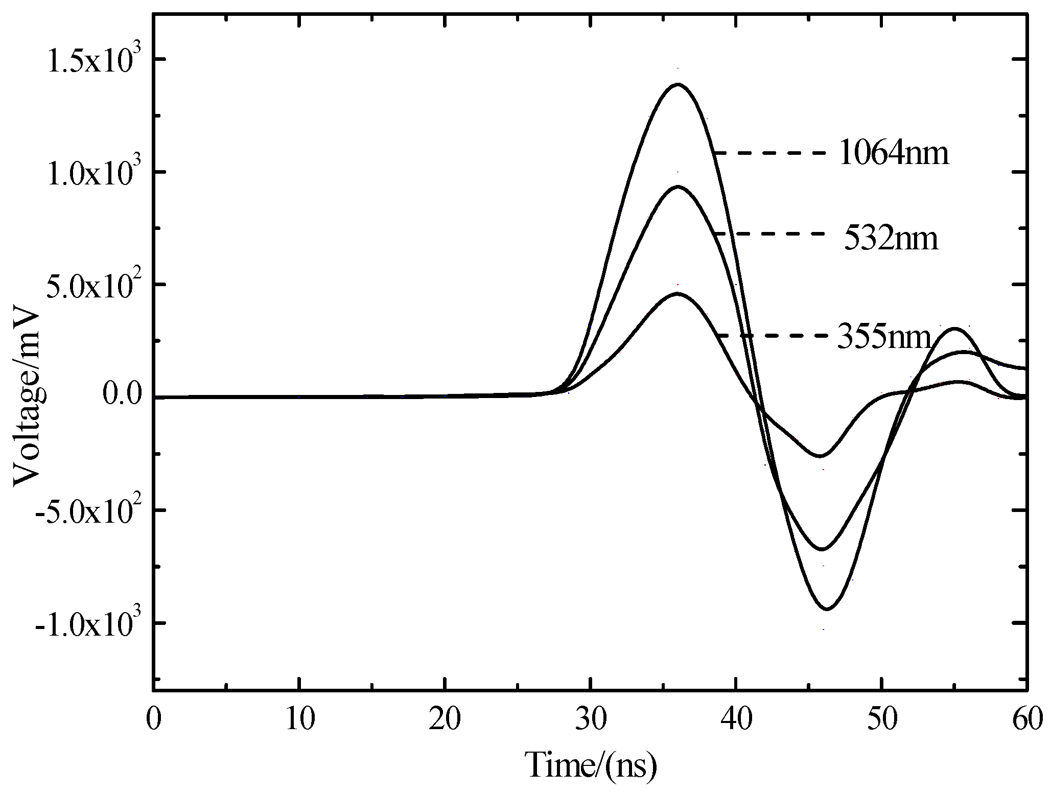
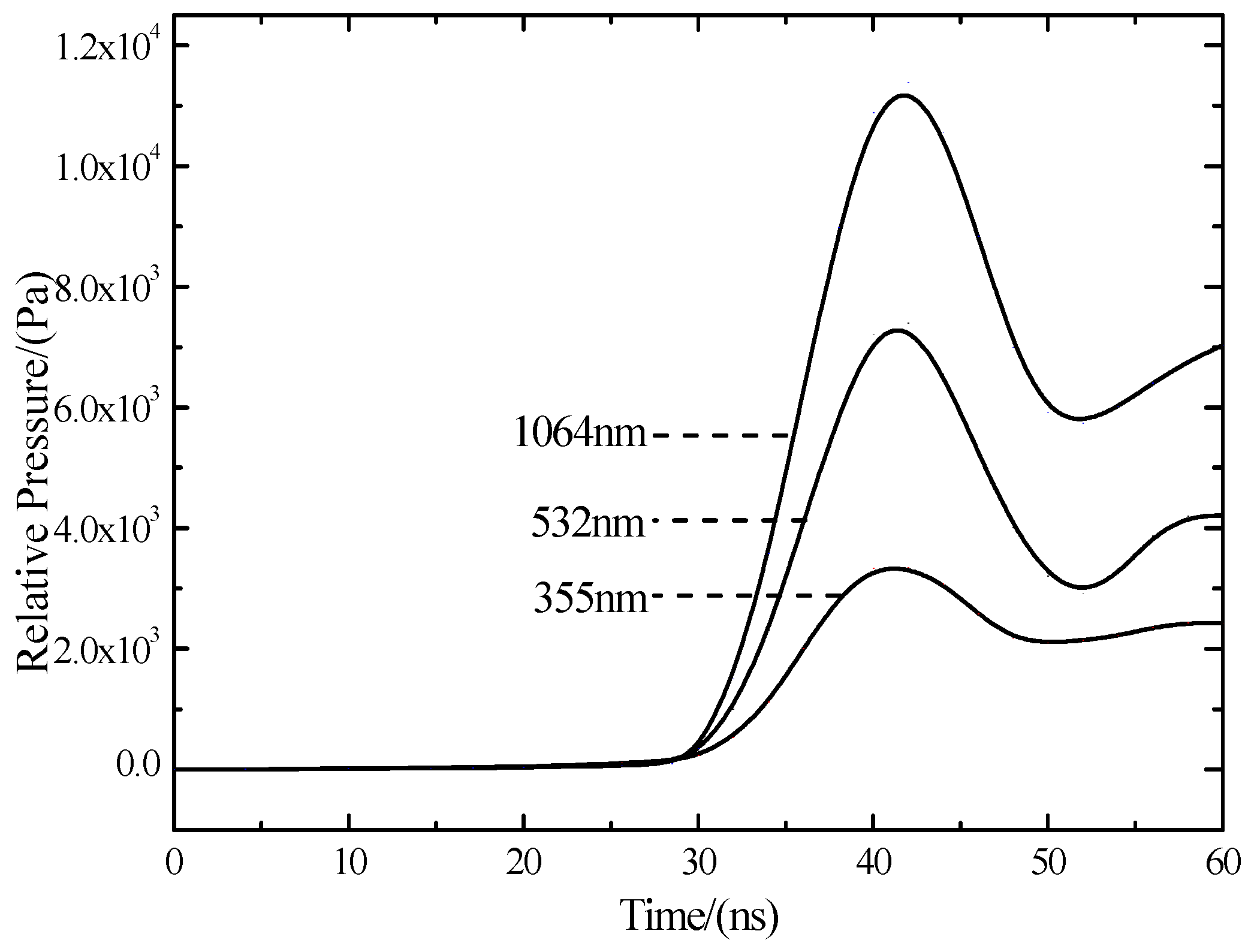
4.2. Effect of Plasma Shock Wave Pressure upon the Surface of the Target
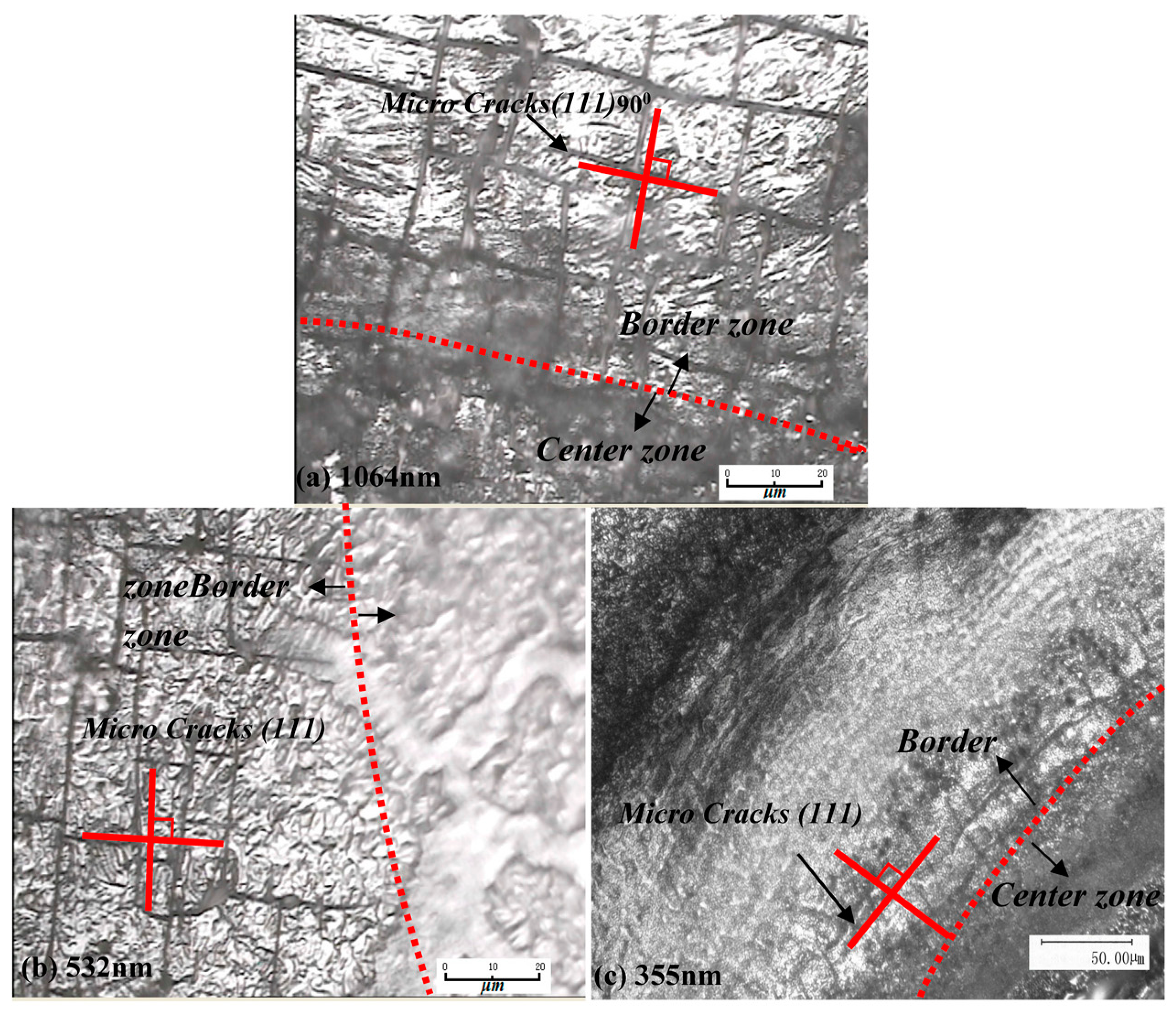
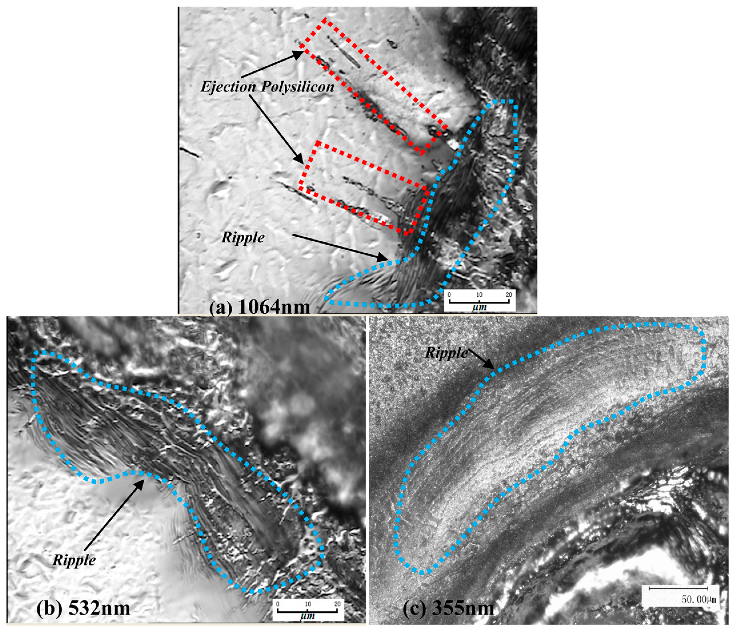
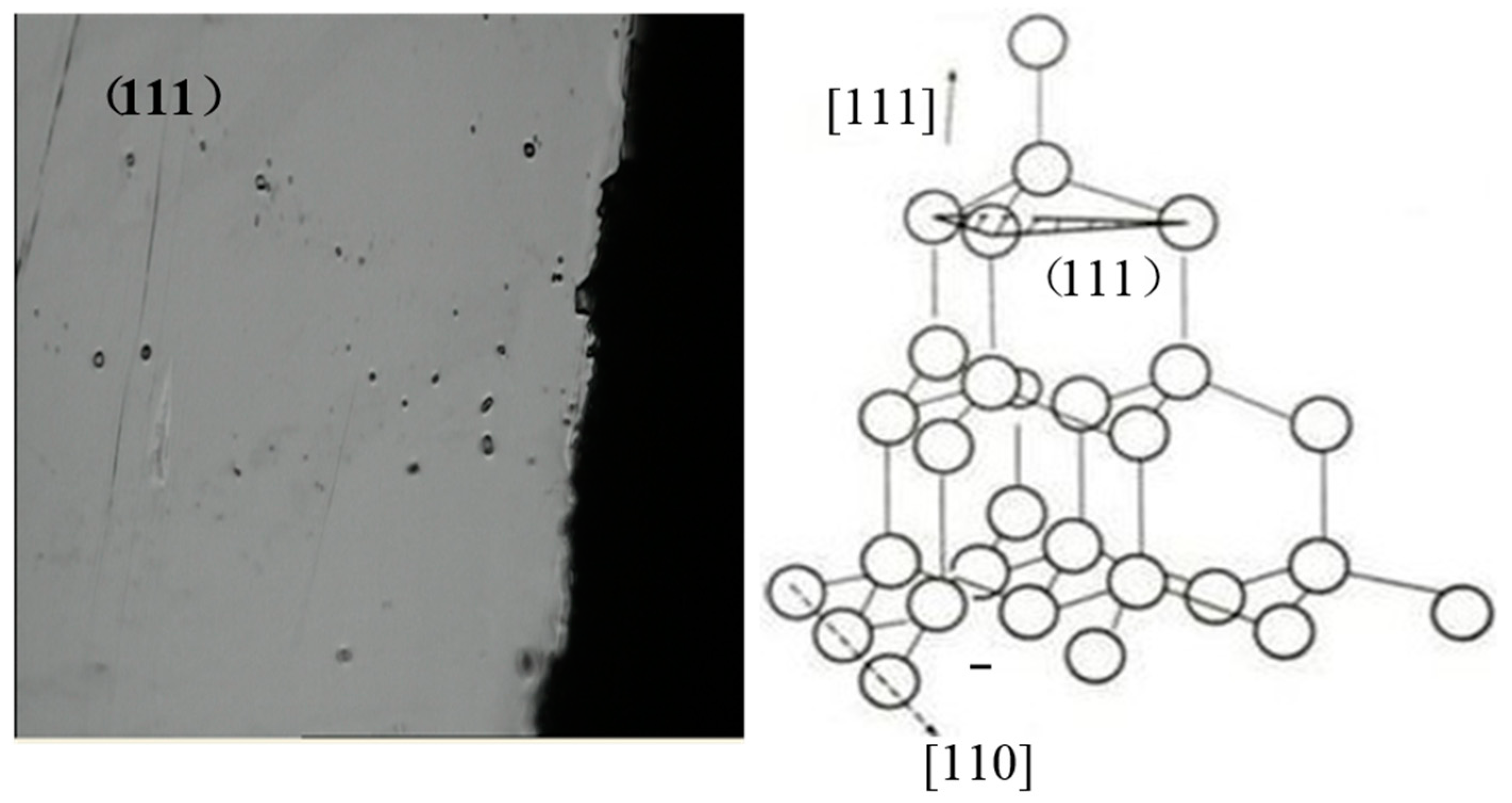
4.2.1. Shock Damage Location of the Target Material Surface under the Laser Thermal
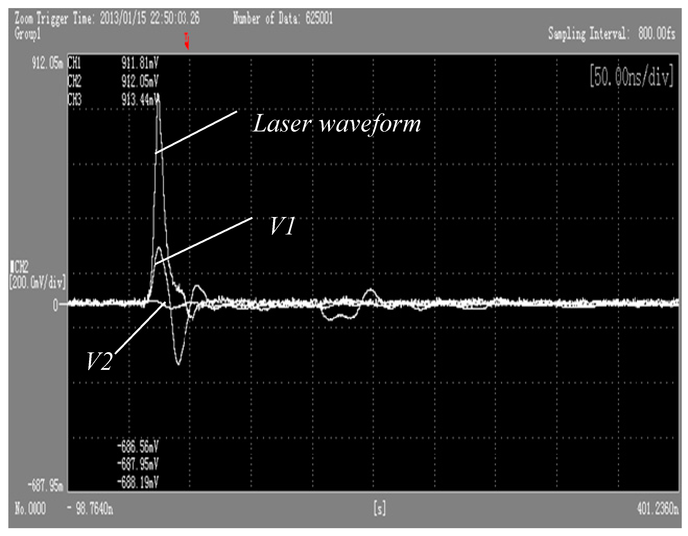
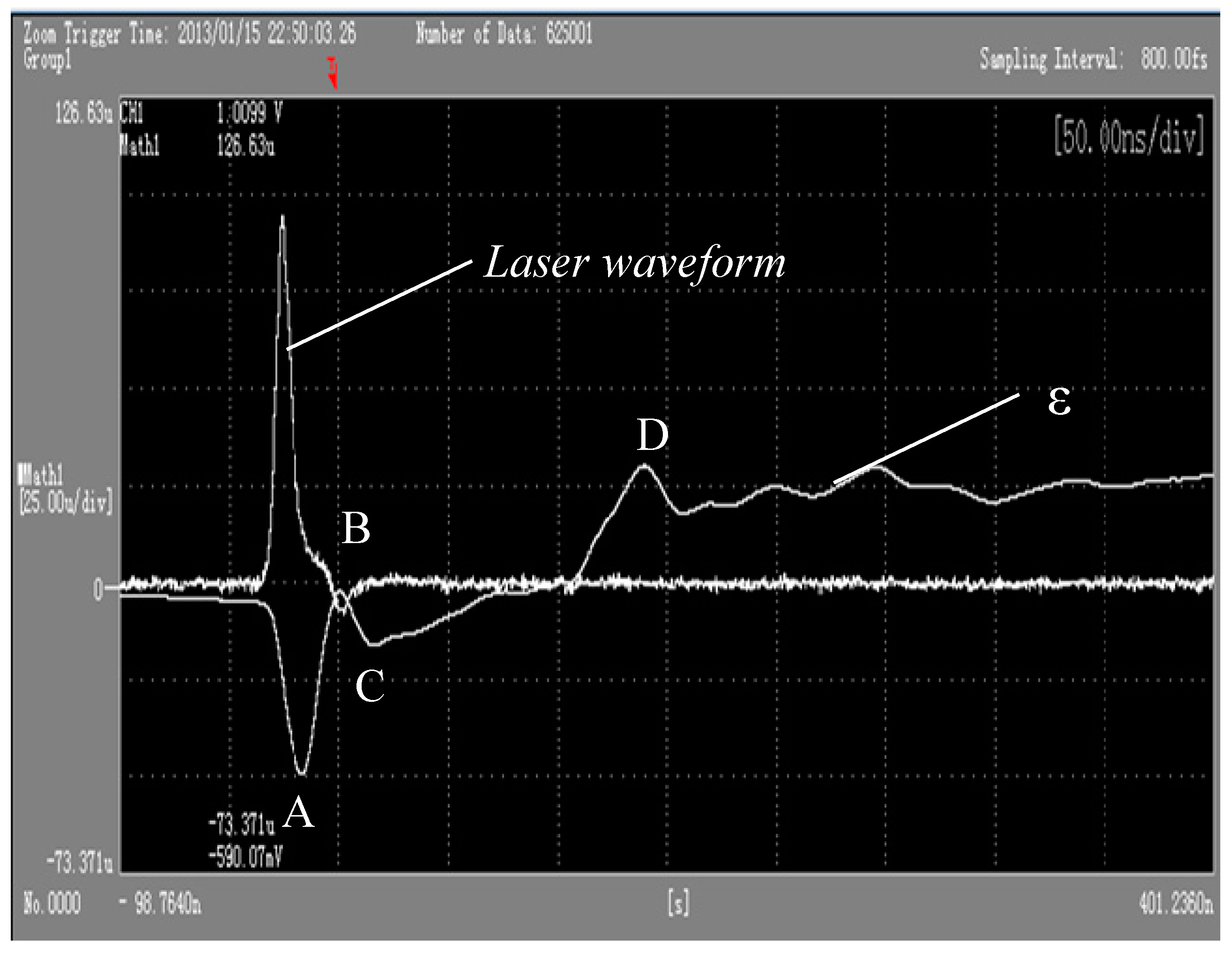
4.2.2. The Dynamic Curve of Laser Shock Wave toward the Target
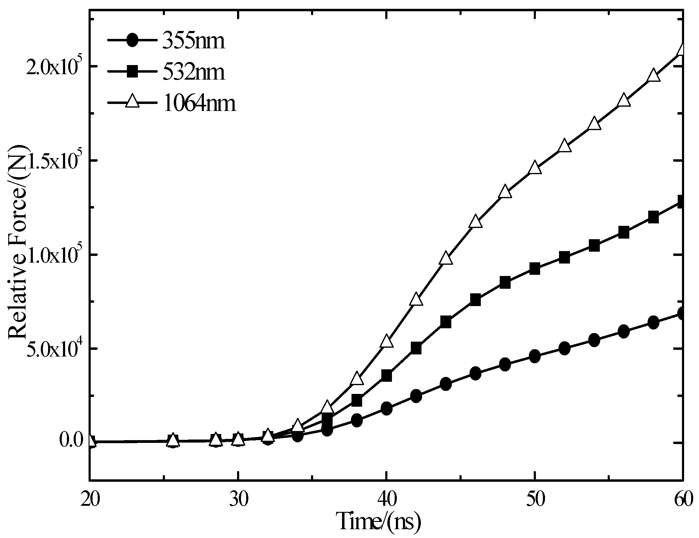
4.2.3. Dynamic Strain of Laser Irradiation Light Spot of Target Edges
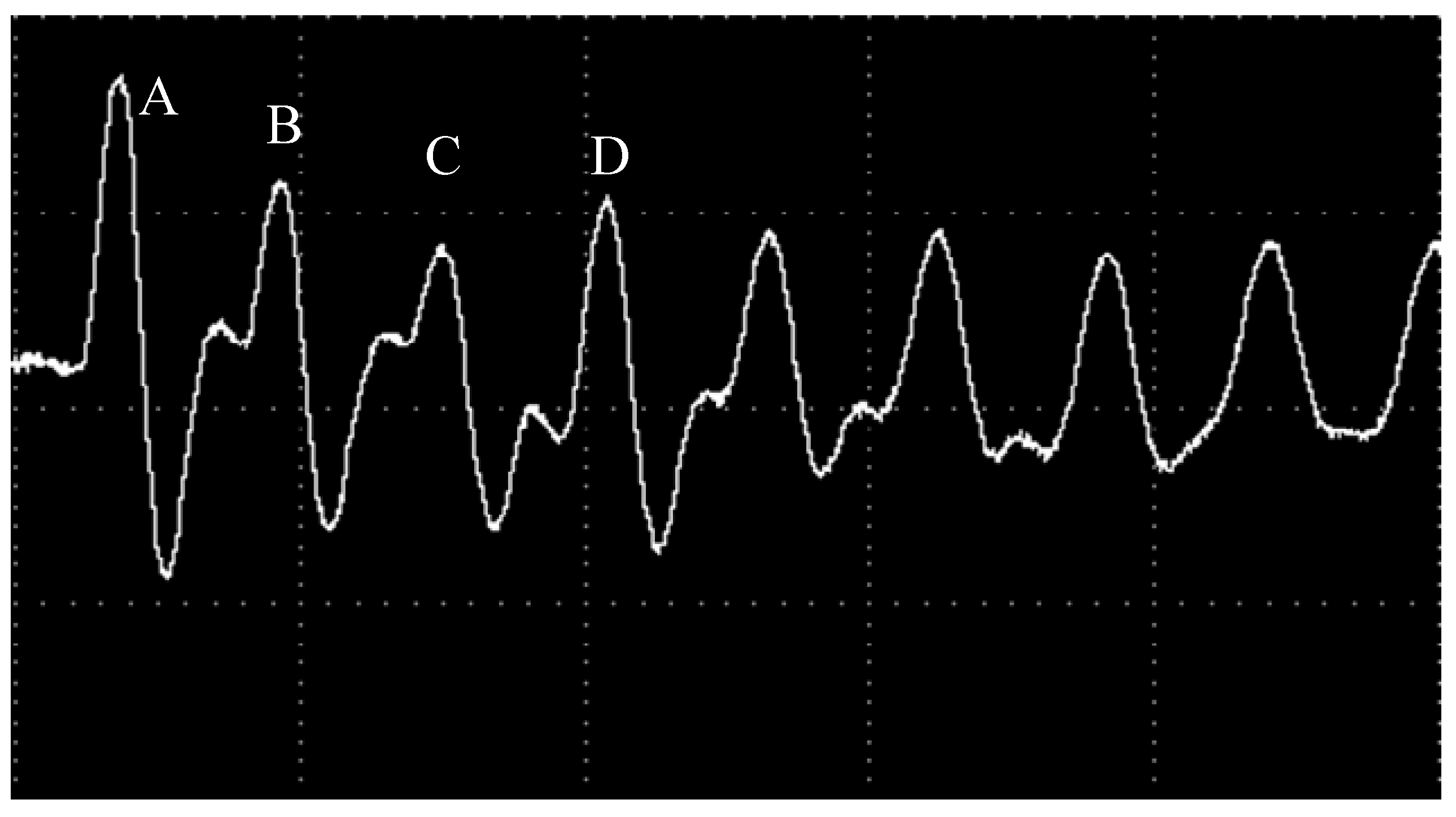
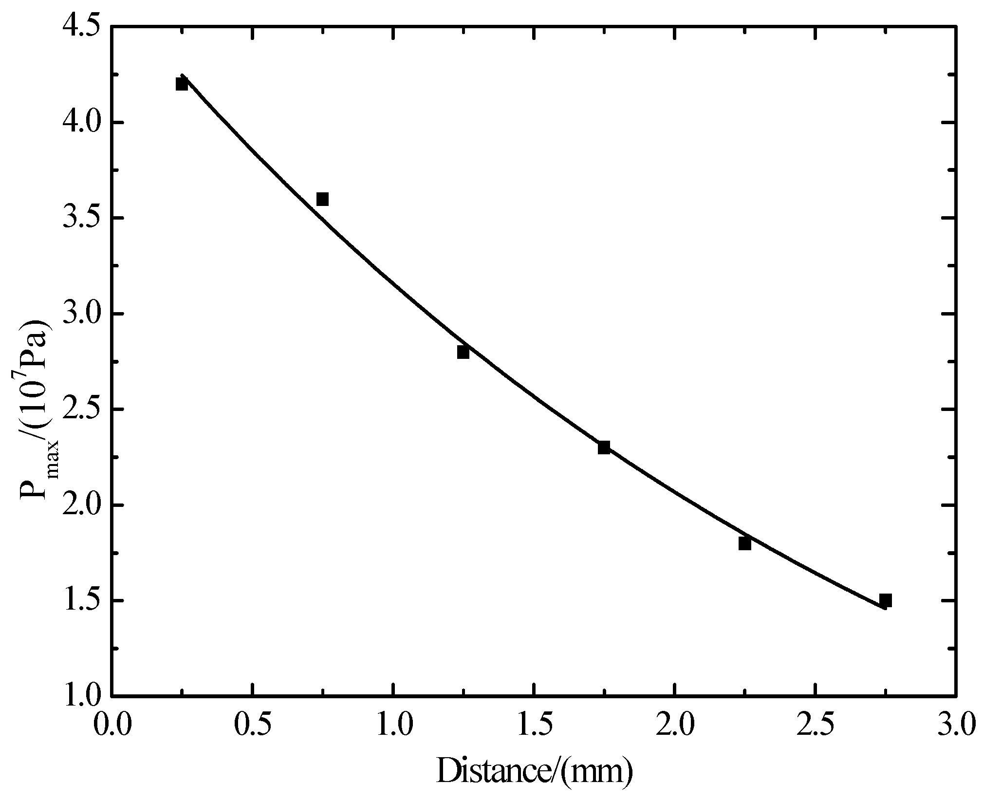
4.3. The Attenuation Rule of Laser Shock Wave in Polysilicon
5. Conclusions
- In the process of pulsed laser action, the combined action of steam pressure and plasma contributes to splash phenomenon of melt, which has a high temperature. In addition, the melting and gasification of polysilicon in the area of laser irradiation provide conditions for the removal of material. Furthermore, the steam pressure and plasma pressure have made great contributions to the removal of material. In addition, the decrease of the laser wavelength enables stronger coupling between laser and target, reducing the breakdown threshold value and weakening laser shock wave strength.
- When the speedily expanding airflow of high pressure stamps melts and couples to the solid part of the target material, recoil pressure will be produced that is perpendicular to the surface, and elastic waves will be composed to form transverse waves on the surface. Furthermore, the spread of transverse waves will cause the deformation of the liquid–solid interface, which is similar to the formation of water waves. At the same time, the tension gradient that is on the surface of the target material causes the phenomenon of moiré, and the higher the temperature of the molten material is, the smaller the surface tension will be; in addition, the lower the temperature is, the greater the surface tension will be. Under the modulated laser irradiation, the liquid on the high temperature zone is pulled into the low temperature zone, which is a result of the coherence and coupling between optics and mechanics.
- Brittle material has a poorer ability to resist shear stress, so it is easy to find the phenomenon of cleavage destruction under the effect of laser shock waves, and the destroyed area is just the edge area of the laser irradiation.
- The average spreading speed of shock waves in the sample of polysilicon is v = 8.47 × 10³ m/s, and the attenuation tendency of the laser shock wave’s pressure peak in polysilicon is in the form of exponential distribution.
Acknowledgments
Author Contributions
Conflicts of Interest
References
- Li, Z.; Zhu, W.; Cheng, J.; Guo, D.; Wu, H. Experimental study of high-power pulsed laser induced shock waves in aluminum targets. Chin. J. Lasers 1997, 24, 259. [Google Scholar]
- Liu, L.; Wang, S.; Wu, H.; Guo, D.; Liao, P. Experimental study of high-power laser induced shock waves. Laser Technol. 2007, 31, 134. [Google Scholar]
- Qi, S. Interaction between Different Wavelengths Laser and Semiconductor Material Hg Cd Te and Si. Master’s Thesis, Changchun University of Science and Technology, Changchun, China, 2010. [Google Scholar]
- Chen, H.; Chang, L.; Jeng, M.; La, C. Characterization of laser carved microchannel polycrystalline silicon solar cell. Solid State Electron. 2011, 61, 23–28. [Google Scholar] [CrossRef]
- Karnakis, D.M. High power single-shot laser ablation of silicon with nanosecond 355 nm. Appl. Surf. Sci. 2006, 252, 7823–7825. [Google Scholar] [CrossRef]
- Dobrzanski, L.A.; Drygała, A. Laser processing of multicrystalline silicon for texturization of solar cells. J. Mater. Proc. Technol. 2007, 191, 228–231. [Google Scholar] [CrossRef]
- Kumar, R.; Mavi, H.S.; Shukla, A.K. Macro and micro-surface morphology reconstructions during laser-induced etching of silicon. Micron 2008, 39, 287–293. [Google Scholar] [CrossRef] [PubMed]
- Huang, M.; Zhao, F.; Cheng, Y.; Xu, Z. Origin of laser-induced near-subwavelength ripples interference between surface plasmons and incident laser. ACS Nano 2009, 3, 4062. [Google Scholar] [CrossRef] [PubMed]
- Zhang, L.; Ni, X.; Lu, J.; Dai, G. Numerical simulation of vaporization effect of long pulsed laser interaction with silicon. Opt. Precis. Eng. 2011, 19, 437–444. [Google Scholar] [CrossRef]
- Kodama, R.; Norreys, P.A.; Mima, K.; Dangor, A.E.; Evans, R.G.; Fujita, H.; Kitagawa, Y.; Krushelnick, K.; Miyakoshi, T.; Miyanaga, N.; et al. Fast heating of ultrahigh-density plasma as a step towards laser fusion ignition. Nature 2001, 412, 798–802. [Google Scholar] [CrossRef] [PubMed]
- Phipps, C.; Turner, T.; Harrison, R.F.; King, T.R. Impulse coupling to targets in vacuum by KrF, HF and CO2 single pulse laser. Appl. Phys. 1988, 64, 1083. [Google Scholar] [CrossRef]
- Ren, J. The Fundamental Physical Mechanisms and Characteristics in Laser Silicon Interaction. Ph.D. Thesis, Stanford University, Stanford, CA, USA, 2005. [Google Scholar]
- Zhang, D.; Li, Z.; Xiao, G.; Guan, L. Kinetic Principle of Pulsed Laser Deposition; Beijing Science Press: Beijing, China, 2011. [Google Scholar]
- Yang, X. A Study on UV Laser Micro-Machining Single-Crystal Silicon. Master’s Thesis, Huazhong University of Science and Technology, Wuhan, China, 2011. [Google Scholar]
- Jellison, G.E.; Lowndes, D.H. Measurement of the optical properties of liquid silicon and germanium using nanosecond time-resolved ellipsometry. Appl. Phys. Lett. 1987, 51, 352. [Google Scholar] [CrossRef]
- Kruer, M.; Allen, R.; Esterowitz, L.; Esterowitz, L.; Bartoli, F. Laser damage in silicon phontodiades. Opt. Quantum Electron. 1976, 8, 453–458. [Google Scholar] [CrossRef]
- Bahu, S.V.; D’Couto, G.C. Excimer laser induced ablation of polyetheretherketone, polyimide, and polytetrafluoroethylene. Appl. Phys. 1992, 72, 692–698. [Google Scholar]
- Chen, C.S.; Liu, A.H.; Sun, G.; Man, B.Y. Analysis of laser damage threshold and morphological changes at the surface of a HgCdTe crystal. Opt. A Pure Appl. Opt. 2001, 8, 88–92. [Google Scholar] [CrossRef]
- Peyre, P.; Berthe, L.; Fabbro, R.; Sollier, A. Experimental determination by PVDF and EMV techniques of shock amplitudes induced by 0.6–3 ns laser pulses in a confined regime with water. J. Phys. D Appl. Phys. 2000, 33, 498. [Google Scholar] [CrossRef]
- Romain, J.P.; Zagouri, F.B.; Bauer, F.; Boustie, M. Measurement of Laser Induced Shock Pressures Using PVDF Gauges; American Institute of Physics: New York, NY, USA, 1994. [Google Scholar]
- Fairand, B.P.; Clauer, A.H.; Jung, R.G.; Wilcox, B.A. Quantitative Assessment of Laser-Induced Stress Waves Generated at Confined Surfaces. Appl. Phys. Lett. 1974, 25, 431–433. [Google Scholar] [CrossRef]
- Bao, L.-D.; Han, J.-H.; Duan, T.; Sun, N.-C.; Gao, X.; Feng, G.-Y.; Yang, L.-M.; Niu, R.-H.; Liu, Q.-X. Investigation of thermodynamics progress of silicon ablated by nanosecond uv repetitive pulse laser. Acta Phys. Sin. 2012, 19, 1–5. [Google Scholar]
- Ma, X. Impact Dynamics; Beijing Institute of Technology Press: Beijing, China, 1992; pp. 57–62. [Google Scholar]


| Thickness/mm | 0.25 | 0.75 | 1.25 | 1.75 | 2.25 | 2.75 |
|---|---|---|---|---|---|---|
| Relative peak voltage/107 Pa | 4.2 | 3.5 | 2.7 | 2.2 | 1.7 | 1.4 |
| Peak voltage withouttransmission loss/107 Pa | 4.2 | 3.6 | 2.8 | 2.3 | 1.8 | 1.5 |
© 2017 by the authors. Licensee MDPI, Basel, Switzerland. This article is an open access article distributed under the terms and conditions of the Creative Commons Attribution (CC BY) license ( http://creativecommons.org/licenses/by/4.0/).
Share and Cite
Xu, J.; Chen, C.; Zhang, T.; Han, Z. A Study of Polycrystalline Silicon Damage Features Based on Nanosecond Pulse Laser Irradiation with Different Wavelength Effects. Materials 2017, 10, 260. https://doi.org/10.3390/ma10030260
Xu J, Chen C, Zhang T, Han Z. A Study of Polycrystalline Silicon Damage Features Based on Nanosecond Pulse Laser Irradiation with Different Wavelength Effects. Materials. 2017; 10(3):260. https://doi.org/10.3390/ma10030260
Chicago/Turabian StyleXu, Jiangmin, Chao Chen, Tengfei Zhang, and Zhenchun Han. 2017. "A Study of Polycrystalline Silicon Damage Features Based on Nanosecond Pulse Laser Irradiation with Different Wavelength Effects" Materials 10, no. 3: 260. https://doi.org/10.3390/ma10030260
APA StyleXu, J., Chen, C., Zhang, T., & Han, Z. (2017). A Study of Polycrystalline Silicon Damage Features Based on Nanosecond Pulse Laser Irradiation with Different Wavelength Effects. Materials, 10(3), 260. https://doi.org/10.3390/ma10030260