Abstract
This paper discusses the near-field inductive coupling wireless power transfer (WPT) at the system level, with detailed analyses on each state-of-the-art WPT output voltage regulation topologies. For device miniaturization and power loss reduction, several novel architectures for efficient WPT were proposed in recent years to reduce the number of passive components as well as to improve the system efficiency or flexibility. These schemes are systematically studied and discussed in this paper. The main contribution of this paper is to provide design guidelines for WPT system design. In addition, possible combinations of the WPT building block configurations are summarized, compared, and investigated for potential new architectures.
1. Introduction
An inductively-coupled wireless power transfer (WPT) system contains nearly all kinds of power converters, including DC-AC converters (inverters, also known as non-linear power amplifiers), transformers (tightly or loosely coupled WPT coils), AC-DC converters (rectifiers), DC-DC converters, and also linear regulators. A non-specific near-field WPT system including most of the building block combinations is shown in Figure 1.
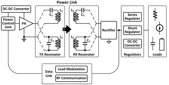
Figure 1.
The block diagram of a non-specific inductive WPT system.
The WPT system consists of a power transmitter (TX) and a power receiver (RX) for an inductive power link, a data up-link (from secondary side to primary side, mainly for the output regulation), and an optional data down-link (from primary side to secondary side). The power link delivers power through the transmitting series or parallel resonator (L1 and C1) which is driven by the power amplifier (PA). The receiving series or parallel resonator (L2 and C2) obtains the wireless power, and then feeds the AC power to the rectifier. The rectifier output conventionally is an unregulated coarse DC voltage with certain level of ripples. Thus, the following regulation stage performs the local voltage regulation using linear series/shunt regulator(s) and/or DC-DC converter(s). The linear regulator can only provide a step-down output voltage than the rectifier output, because its output voltage is controlled by tuning the on-resistance of its power transistor. On the other hand, a DC-DC converter that contains switches and energy storage components (inductors or capacitors) could step-up or step-down its output voltage. But the additional passive components in the DC-DC converter undesirably occupy considerable chip and/or printed circuit board (PCB) area. In addition, the switching operation of DC-DC converters generates output ripples and ground noises. Therefore, tradeoffs should be made in selecting the system architecture and building blocks, while design guidelines on WPT circuits and systems are provided in this paper.
Besides the receiver side local voltage regulation blocks, a global voltage regulation scheme can be realized by feeding the rectifier output information back to the primary side through load modulation or out-band radio frequency (RF) communication (Bluetooth, for example). When the rectifier output information is obtained by the power control unit (PCU) on the primary side, the PCU will decode the feedback data, and then change the PA output power accordingly by adjusting the PA supply voltage which is generated by a DC-DC converter, or by adjusting the duty ratio or amplitude of the input signal of the PA.
The global voltage regulation loop, which involves several main power blocks, is slow compared to the RX local voltage regulation. However, from the efficiency point of view, the global loop is necessary. Because the total power efficiency ηTOTAL of the WPT link is the multiplication of the efficiencies of each stage, as given below:
where ηDC-DC, ηPA, ηLINK, ηRECT, and ηREG are the efficiencies of the DC-DC converter and the PA on the TX side, the efficiency of the coupling link, and the efficiencies of the rectifier and the regulators on the RX side, respectively. When the received power exceeds the demand of the load, the exceeded portion will be consumed by the linear regulator or other over-voltage protection circuits. In such cases, the ηREG is low and will affect the total efficiency. Assume each stage achieves a reasonably good efficiency of 90%, then the total efficiency is only 59%, which is more or less discouraging. Nevertheless, based on the above assumption, if the efficiency of one certain stage increases 2%, the ηTOTAL can be increased by 2% × 59% = 1.18%, which is not bad. Thus, a detailed optimization for “efficiency mining” for each stage is important.
ηTOTAL = ηDC-DC × ηPA × ηLINK × ηRECT × ηREG
As depicted in Figure 1, the inductive coupling coils on both primary and secondary sides can be configured either in series or in parallel with the resonance capacitor. Thus, there are four types of resonance combinations for the inductive power link: series-to-series, series-to-parallel, parallel-to-series, and parallel-to-parallel. The selection of resonance type for high system efficiency depends on the current load level and the coupling coefficient, which would affect the reflected equivalent load impedance on the primary side of the WPT system [1,2,3].
The load of a WPT system could be mixed-signal/digital circuits that are commonly modelled as a resistor in parallel with a capacitor, or analog circuits or neuron stimulation electrodes that can be modelled as a current source, or a rechargeable battery that is similar to a super capacitor. Thus, the regulator design and the system design should fully take the load characteristics into considerations, and specific regulation circuits should be designed for a specified load [4,5]. Sometimes, a high output voltage (say >10 V) is needed for specific applications, such as the neuron stimulation in biomedical implants or the flash memory write operation in a wirelessly powered data storage device. Large winding ratio between L1 and L2 can be simply used to boost the RX output voltage, eliminating one additional step-up DC-DC converter on the RX side.
The paper is organized as follows: Section 2 describes the operation principles of the WPT systems. Then, recent developments on the WPT system architecture and voltage regulation schemes for portable and implantable applications are reviewed and discussed in Section 3. Discussions and future directions are given in Section 4. Finally, conclusions are drawn in the last section.
2. Operation Principles
A well-regulated supply voltage or current is demanded for the load on the secondary side. The simplest way of regulating the output voltage is to use the shunt regulator to bypass the exceeding power to the ground while the PA always transmits its maximum output power. Obviously, in this case, the system efficiency is low when the demanded power of the load is low, while the transmitted power remains unchanged. Thus, the up-link data through load-modulation should be back-scattered to the primary side to adjust the PA output power. In addition, DC-DC converters or linear regulators are added in cascade with the rectifier stage in the conventional designs to provide an accurately regulated output [6,7,8,9]. In many cases, multiple supply voltages are needed for different load circuits, for example, 0.5–1 V for low power digital signal processing circuits, 1.2–1.8 V for analog circuits, and 10–20 V for neuron stimulation or memory circuits. Therefore, multiple-output topologies are also of interest to the WPT systems.
A typical inductive power link example for implantable medical devices is shown in Figure 2. For the RX chip, a shunt regulator provides a coarse voltage regulation and over-voltage protection, and a series-type low-dropout (LDO) regulator provides an essential fine voltage regulation for the load circuits. The back-scattering (data up-link) is realized by largely changing the input impedance of the rectifier (shorting out the two AC inputs, for example) to transmit binary data of the voltage information VDC back to the primary side through the power link carrier. In this case, more energy storage components are required for the RX, since normally no energy will be converted during the load-modulation period. Then, the up-link data is recovered by magnetic sensing of the PA output current through a sensing inductor and a load detector. The data is then used to control the supply voltage of the PA and thus the transmitted output power.
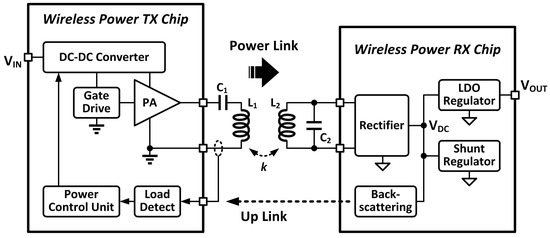
Figure 2.
A typical inductive WPT system with linear regulators and data up-link through load modulation for power control.
For the stability considerations, since multiple low-frequency poles exist in the global voltage regulation loop, contributed by the DC-DC converter, the PA driven inductive link, and the rectifier, etc., an integrator that provides a DC pole 1/s is required in the power control unit to stabilize the global loop. A compensating function that contains zero(s) could also be inserted into the PCU for better phase margin. In addition, when higher WPT frequency and/or DC-DC switching frequency are chosen, smaller passive components can be used in the power converters to increase the frequencies of the non-dominant poles. Consequently, the stability problem of the global loop can be alleviated, the loop bandwidth can be extended, and the transient response can be faster.
The near-field inductive coupling WPT systems can be classified into two categories: the inductive power transfer (IPT) and the resonant wireless power transfer (R-WPT). Both operation modes create the magnetic field by a resonant circuit to transmit power. The IPT requires the coupling coils be placed closely together, and they should be well-aligned for high efficiency. Usually, a magnetic core is also required. Therefore, the IPT systems can operate over a wide range of transmission frequency, as a low Q system eases the requirements on the passive components. For the R-WPT, the coils can be loosely coupled, and thus more spatial freedom can be obtained. In R-WPT, each coil is capacitive loaded forming a tuned LC resonant tank. When both coils have the same resonant frequency, the power transmission distance can be extended with a reasonable efficiency. However, the resonant operation is sensitive to component variation, since the power transmission frequency is a narrow band for high Q, and the efficiency is relatively lower than the IPT operation because of the weak coupling.
Actually, an R-WPT system is pretty much like the topology of a conventional resonant DC-DC converter system, with the transfer in the middle being replaced by a pair of loosely coupled coils. When the switching frequency of the resonant converters exactly coincides with the resonant frequency, the resonant converter operates optimally and can reduce switching loss, and consequently provides high power conversion efficiency. However, when the resonant converter is optimized at one operating point, it is hard to control the output power. In addition, in the R-WPT applications, such as mobile phone charging or powering the implantable medical devices, it is difficult to achieve a resonant condition with cm-sized or mm-sized coils at a low frequency in the kHz range, and a resonant frequency in the MHz range is required.
3. Output Voltage Regulation Schemes
In many state-of-the-art designs, novel system level output voltage regulation schemes were proposed to eliminate the need for a post-conversion stage, and consequently reduce the system complexity and increase the maximum achievable total efficiency [10,11,12,13,14,15,16,17,18,19,20,21,22,23,24,25,26,27]. These schemes are discussed in the following sub-sections.
3.1. Primary Side Non-Linear Power Control
The voltage regulation can be implemented on the primary side with linear control methods (like the amplitude modulation, AM) or with non-linear control methods. With the TX side power control, the regulation blocks in the RX side may not be needed, such that the system total efficiency can be higher. However, the control loop should be fast enough to respond to the load transient on the RX side. Otherwise, the RX side local regulation blocks cannot be removed. In the conventional linear control method, supply voltage of the PA is changed to tune the output power [6,7] because the on-resistance of the switches is almost linearly proportional to its gate-to-source voltage, VGS. To change the PA supply voltage linearly and consequently change the output power, the speed is limited by the large passive components of the DC-DC converter and the resonance power link. Thus, for a faster transient response to the load, primary side non-linear control methods were used in [10,11,12] as discussed below.
Figure 3 illustrates a primary side non-linear control method by changing the PA switching frequency between the LC resonant frequency FRES and its odd-order sub-harmonic frequency FRES/3 [11]. In this system, the energy delivery from the PA to the LC tank is reduced from once every resonant period at the input frequency of FRES to once every three resonant periods at the input frequency of FRES/3, as shown by the conceptual waveforms in Figure 3. Thus, the transmitted powers at these two different input frequencies are changed. Note that, although the input frequency of the PA would vary between FRES and FRES/3, the LC resonance tanks of the power link still always operate at their resonant frequency because the resonant tank is a band-pass filter.
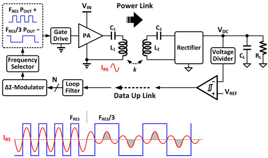
Figure 3.
A WPT system with output power controlled by transmission frequency hopping [11].
The RX power demand signal is obtained by comparing the RX output voltage with a reference voltage, and be fed back to TX side by data up-link. Then, the power demand signal is integrated by a digital loop filter, and is converted to N bits. The information is then processed by a ΔΣ-modulator for frequency domain noise-shaping, in order to generate a frequency-control signal for spurious emission reduction. If the power demand is high, the PA frequency will happen more at FRES. On the contrary, the PA will have more time to operate at FRES/3 if the power demand is low.
A two-transmitter topology was also proposed in [12] for non-linear primary side power control, as shown in Figure 4. Two physically overlapped TX coils L1A and L1B are driven by two separate PAs. In addition, the input clocks of these two PAs have the same frequency but different phases, controlled by a delay-locked loop (DLL). When the power demand signal is fed back to the primary side, the phase select circuit will increase or decrease the phase difference θ between those two clock signals to adjust the combined output power of the two PAs. With larger phase difference, the combined output power is less, and vice versa. The combined output power PO can be approximately expressed as POA × (1 + cosθ), where POA is the output power of a single PA.
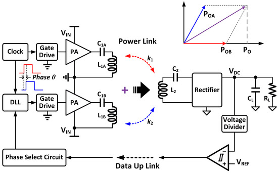
Figure 4.
A WPT system with output controlled by the phase difference of two transmitters [12].
One problem with this two-PA structure is that, although the regulation stage on the RX side is removed for higher total efficiency, the transmission efficiency becomes low as the transmitted power is reduced while the power loss of the transmitter has barely changed.
3.2. Reconfigurable Rectifier for Adaptive Output
In a WPT system without primary side power control, a reconfigurable rectifier that can adapt its operation mode according to output voltage level, which can provide a coarse regulation instead and extend the output power range as demonstrated in [13,14,15]. Figure 5 shows an inductively coupled WPT system with reconfigurable rectifier for low power applications. A hysteresis comparator is used to compare the rectifier DC output voltage with the reference voltage and to decide the reconfigurable rectifier being operated at either mode. The hysteresis window used here is relatively large (say, 1 V), and only 1-bit resolution can be provided by two modes, making the VDC not accurate enough for the load. Thus, an LDO regulator is still needed in such systems for fine regulation.
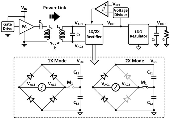
Figure 5.
A WPT system with a reconfigurable rectifier for coarse regulation and transmission distance extension [13,14].
A typical 1X/2X reconfigurable rectifier with passive diodes is also shown in Figure 5. When the mode switch M1 is turned off, the four diodes operate as a full-wave rectifier, noted as the 1X mode. When M1 is turned on, the voltage of VAC2 is clamped to a DC potential, roughly half of the VDC by two capacitors CL1 and CL2. Then, two diodes will operate as a voltage doubler (2X mode) of which the output voltage is roughly two times that of the AC input amplitude, while the other two diodes (in gray color) are constantly-off in this mode. The 2X mode operation can also be understood as two stacked half-wave rectifiers.
Under the same AC input amplitude, the ideal input impedance in the 1X mode operation is four times larger than that in the 2X mode operation when driving the same resistive load. Because the 2X mode ideally provides two times the output voltage, which results in two times the load current and two times the input-to-output current ratio, making four times the input current difference compared to the 1X mode. This impedance transfer characteristic should be taken into account when designing the system operation point. Note that the assumption of the AC amplitude unchanged with the mode change basically does not hold in the WPT system because the equivalent load impedance to the primary side would change with the mode change. Consider the general case illustrated in Figure 6: the load resistor on the RX side is mapped to the primary side as RL,EQ, and the PA has an equivalent output impedance of RS. When RL,EQ equals RS, the output power delivered to the equivalent load PL is the maximum, and the ideal efficiency at this point is 50%. We know that the RL,EQ in 2X mode is smaller than that in 1X mode, and if RL,EQ in 1X mode happens to be smaller than RS (on the left side of the curves), the available output power will decrease when the rectifier changes to 2X mode with further smaller RL,EQ. Thus, to make the reconfigurable rectifier scheme work properly, the system has to operate on the right side of the curves (at low power levels). This limits the scheme only valid for low power applications, like the implantable medical devices for example.
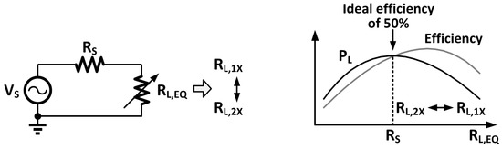
Figure 6.
Illustration of the relationship of load impedance, output power, and efficiency.
In addition, the input reactance of the reconfigurable rectifier will also vary with the mode change. Thus, an adaptive input matching network, which tunes the resonance capacitor automatically, would be helpful for achieving higher efficiency and output power.
With all of the above-mentioned factors being considered, a reconfigurable rectifier provides an alternative power control strategy for extending the output power level, wireless power transmission distance, and increasing system efficiency.
3.3. Resonant Regulating Rectifier
A time domain control method was proposed for resonant DC-DC converter in [16] to adjust the output voltage while still satisfying the optimum operating conditions. By selectively enabling/disabling the converter at an integer multiplier of half cycles, the output power can be tuned by controlling the number or ratio of the enabled and disabled half cycles. The similar idea was applied to the R-WPT application as well, and is discussed as follows.
In a series resonating case as shown in Figure 7, the resonator on the receiver side (L2 and C2) acts as an AC current source supplying the rectifier. A switch M1 with pulse-width modulation (PWM) control is added to the rectifier output to control the output voltage, and is regarded as one-switch resonant regulating rectifier (3R) in [17]. When M1 is on, the resonator is designed to operate in its resonating mode, thus the resonant current IRS starts to increase and is delivered to the load, and VOUT goes up. When M1 is off, no current goes to the load from the rectifier and VOUT decreases, the resonator deviates from its resonating point, and IRS decreases. Thus, by tuning the turn-on duty cycle of M1, the output voltage can be regulated without using additional power converters or linear regulators. The limiting capacitor CLM is used to reduce the voltage peak on node VX preventing the over-voltage condition during the M1 off state. Obviously, this is a discontinuous conduction mode (DCM) topology. Thus, it can only deliver current to the load discontinuously, which results in large peak current of IREC, and degrades the efficiency, since the conduction loss of M1 is given as
where RON is the on-resistances of the M1 and also that of the diodes, T is the operation period, and N is an integer. Thus, reducing the peak current of IREC is definitely favorable for increasing the power conversion efficiency.
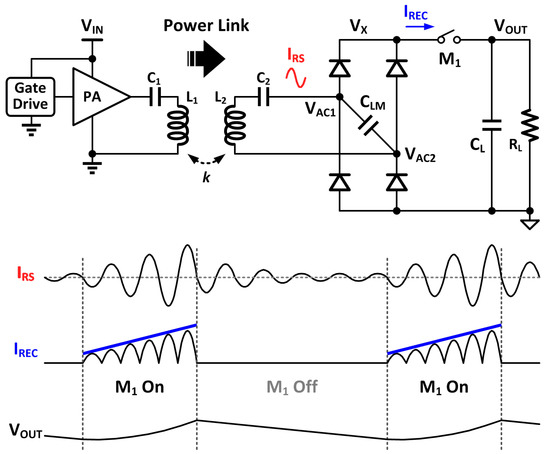
Figure 7.
A resonant WPT system with one-switch pulse-width modulation regulating rectifier.
Consequently, a continuous conduction mode (CCM) was also proposed in [17] with one fly capacitor CFLY and three switches M1–M3, as shown in Figure 8. The CFLY and switches conduct like a step down charge pump. When M1 and M3 are on and M2 is off, CFLY is in parallel with CL, and the full-wave rectifier charges up VOUT. When M1 and M3 are off and M2 is on, CFLY is in series with CL. Then, VX would be roughly two times that of VOUT, and IREC starts to decrease. In the CCM operation, IREC is continuously provided to the load, which results in higher power conversion efficiency and lower output voltage ripples. In addition, the current variations of IRS and IREC are less, relieving the voltage stress on VX, and, consequently, smaller CLM could be used.
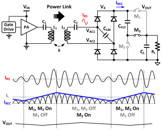
Figure 8.
A resonant WPT system with a pulse-width modulation regulating rectifier and a step-down charge pump [17].
3.4. Reconfigurable Regulating Rectifiers
Based on the knowledge of the two sub-sections above, a reconfigurable 1X/2X regulating rectifier was designed in [18] as illustrated in Figure 9. The reconfiguration switch M1 is now controlled by a PWM signal as well. When M1 is on, the rectifier operates in 2X mode as described in Section 3.2. Thus, the VOUT will be increasing and intends to reach two times that of VAC,Peak. When M1 is on, the rectifier operates in 1X mode and the ideal output in this case is VAC,Peak. Thus, the VOUT will be decreasing. The waveforms plotted in Figure 9 show the CCM case, and, of course, the regulating rectifier can operate in DCM at light-load conditions as well. In such a way, the output can be well regulated in different load conditions.
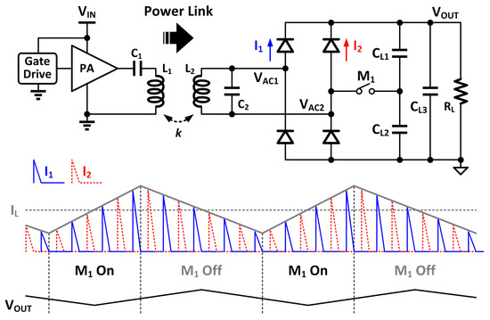
Figure 9.
A WPT receiver with a 1X/2X regulating rectifier with pulse-width modulation [18].
One more advanced version of the reconfigurable regulating rectifier was proposed in [19] as shown in Figure 10. This reconfigurable rectifier has three modes: 1X, ½X, and 0X modes. In the 1X mode, both M1 and M2 are off, and it operates as a full-wave rectifier that can provide large output current to the load. In the ½X mode, M1 is on and M2 is off, and VAC2 is shorted to the ground. Then, only one diode out of the four will conduct current I1 to the load as a half-wave rectifier. Compared to the 1X mode, the current delivered to the load is half, thus this mode is named as ½X. In the 0X mode, different from the M1 off-state in the one-switch 3R operation, both M1 and M2 are on, and the receiving resonant tank L2 and C2 is freewheeling, while the rectifier is open in the 3R case.
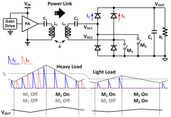
Figure 10.
A WPT receiver with a 1X/½X/0X regulating rectifier with pulse-width modulation [19].
The output regulation of the above topology can be achieved by switching between two of the three modes, which means a finer regulation. In heavy load conditions, 1X and ½X modes are selected. In light-load conditions, ½X and 0X modes can be selected. Therefore, CCM operations can be maintained for a wide load current range. A smooth transition between different modes during load transient can be achieved with accurate load current sensing techniques, which add some circuit complexity to the on-chip implementation.
3.5. Pre-Rectifier Regulation
Besides the above-mentioned primary side power control and reconfigurable and/or regulating rectifiers topologies for output regulation, pre-rectifier regulation topology was proposed in [20,21], as demonstrated in Figure 11. Similar to the previous load modulation schemes that switch rectifier modes with PWM signals, the pre-rectifier regulation scheme (named as Q-modulation in [20]) tried to modulate the load impedance seen from the resonator, and thus to achieve output regulation.
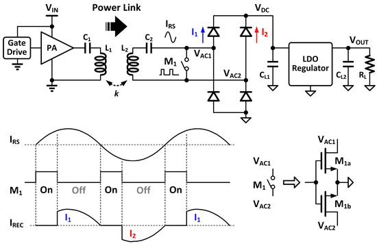
Figure 11.
A WPT receiver with PWM pre-rectifier regulation [20,21].
As shown by the conceptual waveforms in Figure 11, the switch M1 will be turned on at the zero-crossing point of the resonating current IRS, which is commonly known as zero-current switching (ZCS). To avoid the switch experiences of high voltage and current simultaneously, which causes unnecessary conduction loss, ZCS is an important operation principle for high efficiency. During the M1 on-state, the high-Q resonant tank L2 and C2 stores the maximum energy that is transferrable from the primary side. During the M1 off-state, the energy stored in the resonant tank together with the new coming transferred energy is delivered to the load through I1 and I2 of the rectifier. Therefore, the amount of energy that transferred to the load can be controlled by tuning the on-duty cycle D of the switch. Different from the above-mentioned regulation schemes, this scheme achieved the regulation within one cycle at the WPT frequency, requiring faster control circuits (faster transistors).
The maximum input amplitude (carrier envelope) is tracked by a dedicated feedback loop as designed in [20], such that the D will be increased or decreased accordingly. Since the loop only tracks the input voltage, an LDO regulator is still needed for an accurate output voltage. On the other hand, in [21], the rectifier output had been used to be compared with a reference voltage to generate the PWM signal, such that no LDO regulator was used.
In fact, this topology and its operation principle are similar to a resonant DC-DC Boost converter, in which the inductor accumulates energy first and then delivers the energy to the load through a diode. The switch M1 can be implemented by N-type transistors with a reference to the ground potential, as shown in Figure 11. The equivalent input impedance RL,EQ seen from the LC resonant tank can be approximately denoted as
where M = 1/(1 − D) is the conversion ratio of boost converter. The full-wave rectifier converts the RL into (8/π2)RL, assuming the LDO regulator is ideal. With a PWM feedback loop, the Q-modulation technique can transform the load impedance automatically for any load and coupling distance variations.
Based on the same system architecture shown in Figure 11, besides the above-mentioned regulation scheme that performs regulation within every WPT clock period, there are also recent works that perform regulation among multiple WPT clock cycles [22,23]. In such a scheme, the switch M1 is closed for a certain number of cycles to obtain higher resonant voltage amplitude and to accumulate energy in the LC tank, and then M1 is open for a short period of time that is less than one cycle to release the energy stored in the LC tank to the output capacitor. This technique allows a longer transmission distance and harvests more energy in ultra-low power cases.
3.6. Multi-Level Single-Inductor Multiple-Output Operation
In many applications, different supply levels are required by the system for various functions [27,28], while the ripples generated by the converters should be reasonably small for the noise-sensitive loads. Therefore, the bulky passive components in the converters should be utilized effectively [14] or even be reused with time multiplexing. In multiple-output scenarios, single-inductor multiple-output (SIMO) architecture can be employed for minimized number of magnetic components [28,29]. A multi-level SIMO operation for the WPT RX was proposed in [27], which merged a multi-level SIMO DC-DC converter with a Dickson-type multi-stage rectifier as shown in Figure 12.
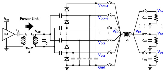
Figure 12.
A WPT receiver with a Dickson-type multi-stage rectifier merged with a multi-level SIMO converter [27].
In such a configuration, any output terminals that need a voltage between VDCn and VDC(n−1) (n = 1, 2, 3, …, N) could be realized by sourcing currents from those two corresponding DC outputs through L3 similar to a Buck converter. Then, the voltage cross L3 can be smaller than that of the typical two-level operation. Therefore, both the inductor current and output voltage ripples can be reduced. In addition, the voltage boosting function is realized by the multi-stage rectifier, and not by a Boost converter, which has the undesirable right-half-plane (RHP) zero. Favorably, a Buck converter can achieve a higher loop bandwidth more easily compared to the Boost or Buck-Boost converters.
To demonstrate the idea, a three-level single-inductor dual-output (SIDO) DC-DC converter was designed for the WPT RX [27], which synergizes with an active voltage doubler and generates three DC levels (including the Gnd). As shown in Figure 13, VO2 draws current from VDC2 and VDC1, and, consequently, provides an output voltage between those two voltages. On the other hand, VO1 draws current from VDC1 and Gnd, and delivers an output voltage lower than VDC1. Therefore, two separate regulated output voltages are obtained from three voltage levels through one inductor L3.
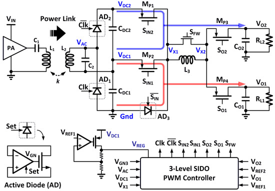
Figure 13.
A WPT system with a voltage doubler and a three-level SIDO converter [27].
To reduce the size of L3, the SIDO converter also switches at 6.78 MHz, which is the WPT frequency. Meanwhile, by synchronizing the operation of the voltage doubler and the SIDO converter, part of the pulsing output currents of the voltage doubler will go to the SIDO converter directly, bypassing the intermediate filtering capacitors CDC1 and CDC2. Consequently, the output ripples can be further reduced. To minimize the cross-regulation problem that is associated with all of the SIMO converters, a small value of L3 should be chosen to keep the converter operating in discontinuous conduction mode (DCM).
The voltage and current waveforms of the three-level SIDO converter operating in DCM is given in Figure 14. The clock signal can be simply recovered from VAC by an inverter, and the short pulse Clk’ that sets the starting point of the PWM control for VO1 can be obtained by a pulse generator [27]. A pulse of the zero current detection signal (ZCD’) that initiates another PWM control for VO2 can be obtained by sensing the drain current of MP2 with a comparator detecting the MP2 source and drain voltages, and it determines the inductor current goes to VO1 or VO2 by swapping the control signals SO2 and SO1. Because both VO2 and VO1 get current from VDC1, MP2 should be kept on during the SO2 and SO1 transition period to reduce the switching loss of MP2. For an accurate detection, a large static current of the comparator is needed for fast speed and for the optimum SO2 and SO1 switch timing. Alternatively, an additional low bandwidth adaptive loop that dynamically adjusts the comparator artificial offset for delay compensation can significantly relax the speed requirement of the comparator, as designed in [3]. Because the adaptive loop only needs a very low loop bandwidth, 200 kHz in [3] for example, it only consumes the current on the order of 1 μA. To attenuate the undesired voltage ringing caused by L3 and the parasitic capacitors on VX1 and VX2 nodes when either of them are floating, a freewheel switch [29] SFW will be turned on when both AD3 and MP4 are off at the end of each cycle. On the other hand, for higher conversion efficiency and/or large output power capability of the SIMO converter, lower switching frequency should be used [30].
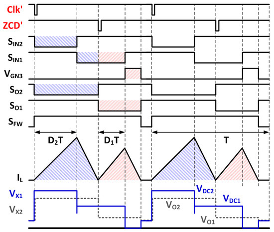
Figure 14.
Voltage and current waveforms of the three-level SIDO converter operating in DCM [27].
4. Discussions and Future Directions
For the WPT systems, as reviewed in this paper at the system level, output voltage regulation can be achieved by the primary side power control, the reconfigurable/regulating rectifiers, as well as the pre-rectifier regulation topologies, or simply cascading a DC-DC converter stage in the RX. For the regulating rectifiers and the pre-rectifier regulation schemes, pulse-width modulation is commonly applied similar to the DC-DC converters for an accurate output regulation. The equivalent load impedance is automatically tuned with the dedicated PWM loop that adapts to the load and coupling distance/orientation variations. Consequently, high efficiencies can be achieved for the WPT receiver and also the entire WPT system.
Besides the above-mentioned equivalent load impedance modulation technique, there are two more direct ways to further improve the WPT system efficiency. One is to achieve the goal at the circuit level, that is, to improve the efficiencies of each cascading power stages. Taking the active rectifier design as an example, optimizing the size of the cross-connected (CC) transistors can elevate the efficiency level because the parasitic capacitors of the CC transistors are actually part of the resonant tank that do not cause switching loss [31]. The other feasible solution is to reduce the number of converter stages. For example, a wireless charger can be designed without a post-stage DC-DC charger [32], but directly charges the battery or super-capacitor through a rectifier only. In such a case, the system regulation loop should process the information of charging current instead of output voltage. Favorably, one stage of conversion loss can be eliminated. Then, of course, sensing of the average AC charging current would be a challenge for the circuit designer.
In terms of device volume, bulky passive components in the AC-DC and DC-DC converters should be utilized effectively or be reused with time multiplexing for miniaturized devices. In addition, operating at a higher WPT frequency can lead to significant size reduction of passive components. Increasing the operation frequency by n times will reduce both the inductor and capacitor values by n times for both the WPT TX and RX because the resonant frequency FRES is determined by
In addition, smaller inductance with higher Q can be more easily achieved at higher frequencies within a limited space, which is one of the key factors for improving the WPT link efficiency.
Last but not least, like all the other analog circuit designs, a dedicated feedback loop controlling the critical parameter is essential for a good WPT design. For instance, a capacitor bank for resonant frequency tuning on the RX side would be very helpful for the maximizing the system efficiency, especially for the resonant WPT operation. Meanwhile, for a robust operation, a WPT system that has multiple loops needs to be investigated carefully and thoroughly on the dynamics of each local (fast) and global (slow) loop.
5. Conclusions
Selecting an appropriate WPT system architecture for portable or implantable applications is a tradeoff between device volume, efficiency, regulation accuracy and speed, and functionality. Different from the conventional single-stage power converter designs, WPT system design involves multiple closely related design parameters, which significantly complicated the scenario and imposes design challenges to the circuit and system designers. State-of-the-art highly-integrated WPT system architectures are comprehensively investigated and discussed in this paper. With considerations from multiple aspects, potential solutions are pointed out for engineers and researchers in this area, and a broad range of promising research opportunities are enabled.
Acknowledgments
This research is supported by the Research Committee of the University of Macau under grant MYRG2015-00107-AMSV, and the Macau Science and Technology Development Fund (FDCT).
Author Contributions
Both authors conceived the work. The paper was written by Yan Lu, and revised by both authors.
Conflicts of Interest
The authors declare no conflict of interest.
References
- Wang, C.-S.; Covic, G.A.; Stielau, O.H. Power transfer capability and bifurcation phenomena of loosely coupled inductive power transfer systems. IEEE Trans. Ind. Electron. 2004, 51, 148–157. [Google Scholar] [CrossRef]
- Ahn, D.; Hong, S. Wireless Power Transmission with Self-Regulated Output Voltage for Biomedical Implant. IEEE Trans. Ind. Electron. 2014, 61, 2225–2235. [Google Scholar] [CrossRef]
- Cheng, L.; Ki, W.H.; Lu, Y.; Yim, T.S. Adaptive On/Off Delay-Compensated Active Rectifiers for Wireless Power Transfer Systems. IEEE J. Solid State Circuits 2016, 51, 712–723. [Google Scholar]
- Lee, H.-M.; Park, H.; Ghovanloo, M. A Power-Efficient Wireless System with Adaptive Supply Control for Deep Brain Stimulation. IEEE J. Solid State Circuits 2013, 48, 2203–2216. [Google Scholar] [CrossRef] [PubMed]
- Lee, H.-M.; Ghovanloo, M. A Power-Efficient Wireless Capacitor Charging System through an Inductive Link. IEEE Trans. Circuits Syst. II Exp. Briefs 2013, 60, 707–711. [Google Scholar] [CrossRef] [PubMed]
- Wang, G.; Liu, W.; Sivaprakasam, M.; Kendir, G. Design and analysis of an adaptive transcutaneous power telemetry for biomedical implants. IEEE Trans. Circuits Syst. I Regul. Pap. 2005, 52, 2109–2117. [Google Scholar] [CrossRef]
- Li, X.; Lu, Y.; Tsui, C.-Y.; Ki, W.-H. An Adaptive Wireless Powering and Data Telemetry System for Optic Nerve Stimulation. In Proceedings of the IEEE International Symposium on Circuits and Systems, ISCAS 2014, Melbourne, Australia, 1–5 June 2014; pp. 1404–1407.
- Park, H.; Jang, J.; Kim, H.; Park, Y.; Oh, S.; Pu, Y.; Hwang, K.C.; Yang, Y.; Lee, K. A Design of a Wireless Power Receiving Unit with a High-Efficiency 6.78-MHz Active Rectifier Using Shared DLLs for Magnetic-Resonant A4 WP Applications. IEEE Trans. Power Electron. 2016, 31, 4484–4498. [Google Scholar] [CrossRef]
- Moti, K.-G.; Neri, F.; Moon, S.; Yeon, P.; Yu, J.; Cheon, Y.; Roh, Y.; Ko, M.; Park, B.-H. A Fully Integrated 6W Wireless Power Receiver Operating at 6.78MHz with Magnetic Resonance Coupling. In Proceedings of the IEEE International Solid-State Circuits Conference (ISSCC), Digest of Technical Papers, San Francisco, CA, USA, 22–26 February 2015; pp. 1–3.
- Radecki, A.; Chung, H.; Yoshida, Y.; Miura, N.; Shidei, T.; Ishikuro, H.; Kuroda, T. 6W/25mm2 Inductive Power Transfer for Non-Contact Wafer-Level Testing. In Proceedings of the IEEE International Solid-State Circuits Conference (ISSCC), Digest of Technical Papers, San Francisco, CA, USA, 20–24 February 2011; pp. 230–232.
- Shinoda, R.; Tomita, K.; Hasegawa, Y.; Ishikuro, H. Voltage-Boosting Wireless Power Delivery System with Fast Load Tracker by ΔΣ-Modulated Sub-Harmonic Resonant Switching. In Proceedings of the IEEE International Solid-State Circuits Conference (ISSCC), Digest of Technical Papers, San Francisco, CA, USA, 19–23 February 2012; pp. 288–290.
- Tomita, K.; Shinoda, R.; Kuroda, T.; Ishikuro, H. 1-W 3.3–16.3-V Boosting Wireless Power Transfer Circuits with Vector Summing Power Controller. IEEE J. Solid State Circuits 2012, 47, 2576–2585. [Google Scholar] [CrossRef]
- Lee, H.-M.; Ghovanloo, M. An Adaptive Reconfigurable Active Voltage Doubler/Rectifier for Extended-Range Inductive Power Transmission. IEEE Trans. Circuits Syst. II Exp. Briefs 2012, 59, 481–485. [Google Scholar] [CrossRef]
- Lu, Y.; Li, X.; Ki, W.-H.; Tsui, C.-Y.; Yue, C.P. A 13.56 MHz Fully Integrated 1X/2X Active Rectifier with Compensated Bias Current for Inductively Powered Devices. In Proceedings of the IEEE International Solid-State Circuits Conference (ISSCC), Digest of Technical Papers, San Francisco, CA, USA, 17–21 February 2013; pp. 66–67.
- Lee, H. An Auto-Reconfigurable 2×/4× AC-DC Regulator for Wirelessly Powered Biomedical Implants With 28% Link Efficiency Enhancement. IEEE Trans. Very Large Scale Integr. (VLSI) Syst. 2016, 24, 1598–1602. [Google Scholar] [CrossRef]
- Joung, G.B.; Rim, C.T.; Cho, G.H. Integral cycle mode control of the series resonant converter. IEEE Trans. Power Electron. 1989, 4, 83–91. [Google Scholar] [CrossRef]
- Choi, J.-H.; Yeo, S.-K.; Park, S.; Lee, J.-S.; Cho, G.-H. Resonant Regulating Rectifiers (3R) Operating for 6.78 MHz Resonant Wireless Power Transfer (RWPT). IEEE J. Solid State Circuits 2013, 48, 2989–3001. [Google Scholar] [CrossRef]
- Li, X.; Tsui, C.-Y.; Ki, W.-H. A 13.56 MHz Wireless Power Transfer System with Reconfigurable Resonant Regulating Rectifier and Wireless Power Control for Implantable Medical Devices. IEEE J. Solid State Circuits 2015, 50, 978–989. [Google Scholar] [CrossRef]
- Cheng, L.; Ki, W.H.; Wong, T.T.; Yim, T.S.; Tsui, C.Y. A 6.78MHz 6W Wireless Power Receiver with a 3-Level 1 ×/½ ×/0× Reconfigurable Resonant Regulating Rectifier. In Proceedings of the IEEE International Solid-State Circuits Conference (ISSCC), Digest of Technical Papers, San Francisco, CA, USA, 31 January–4 February 2016; pp. 376–377.
- Kiani, M.; Lee, B.; Yeon, P.; Ghovanloo, M. A Q-Modulation Technique for Efficient Inductive Power Transmission. IEEE J. Solid State Circuits 2015, 50, 2839–2848. [Google Scholar] [CrossRef] [PubMed]
- Ahn, D.; Kim, S.; Moon, J.; Cho, I.K. Wireless Power Transfer with Automatic Feedback Control of Load Resistance Transformation. IEEE Trans. Power Electron. 2016, 31, 7876–7886. [Google Scholar] [CrossRef]
- Choi, M.; Jang, T.; Jeong, J.; Jeong, S.; Blaauw, D.; Sylvester, D. A Current-Mode Wireless Power Receiver with Optimal Resonant Cycle Tracking for Implantable Systems. In Proceedings of the IEEE International Solid-State Circuits Conference (ISSCC), Digest of Technical Papers, San Francisco, CA, USA, 31 January–4 February 2016; pp. 372–373.
- Gougheri, H.S.; Kiani, M. Current-Based Resonant Power Delivery With Multi-Cycle Switching for Extended-Range Inductive Power Transmission. IEEE Trans. Circuits Syst. I Regul. Pap. 2016, 63, 1543–1552. [Google Scholar] [CrossRef]
- Lee, B.; Kiani, M.; Ghovanloo, M. A Triple-Loop Inductive Power Transmission System for Biomedical Applications. IEEE Trans. Biomed. Circuits Syst. 2016, 10, 138–148. [Google Scholar] [CrossRef] [PubMed]
- Zhao, J.; Yao, L.; Xue, R.F.; Li, P.; Je, M.; Xu, Y.P. An Integrated Wireless Power Management and Data Telemetry IC for High-Compliance-Voltage Electrical Stimulation Applications. IEEE Trans. Biomed. Circuits Syst. 2016, 10, 113–124. [Google Scholar] [CrossRef] [PubMed]
- Lee, K.F.E. A Timing Controlled AC-DC Converter for Biomedical Implants. In Proceedings of the IEEE International Solid-State Circuits Conference (ISSCC), Digest of Technical Papers, San Francisco, CA, USA, 7–11 February 2010; pp. 128–129.
- Lu, Y.; Huang, M.; Cheng, L.; Ki, W.H.; Seng-Pan, U.; Martins, R.P. A Dual-Output Wireless Power Transfer System with Active Rectifier and Three-Level Operation. IEEE Trans. Power Electron. 2017, 32, 927–930. [Google Scholar] [CrossRef]
- Ma, D.; Ki, W.-H.; Tsui, C.; Mok, P.K.T. Single-inductor multiple-output switching converters with time-multiplexing control in discontinuous conduction mode. IEEE J. Solid State Circuits 2003, 38, 89–100. [Google Scholar]
- Ma, D.; Ki, W.-H.; Tsui, C. A pseudo-CCM/DCM SIMO switching converter with freewheel switching. IEEE J. Solid State Circuits 2003, 38, 1007–1014. [Google Scholar]
- Jing, X.; Mok, P.K.T.; Lee, M.C. A Wide-Load-Range Constant-Charge-Auto-Hopping Control Single-Inductor-Dual-Output Boost Regulator with Minimized Cross-Regulation. IEEE J. Solid State Circuits 2011, 46, 2350–2362. [Google Scholar] [CrossRef]
- Lu, Y.; Ki, W.-H. A 13.56 MHz CMOS Active Rectifier with Switched-Offset and Compensated Biasing for Biomedical Wireless Power Transfer Systems. IEEE Trans. Biomed. Circuits Syst. 2014, 8, 334–344. [Google Scholar]
- Lazaro, O.; Rincón-Mora, G.A. 180-nm CMOS Wideband Capacitor-Free Inductively Coupled Power Receiver and Charger. IEEE J. Solid State Circuits 2013, 48, 2839–2849. [Google Scholar] [CrossRef]
© 2016 by the authors; licensee MDPI, Basel, Switzerland. This article is an open access article distributed under the terms and conditions of the Creative Commons Attribution (CC-BY) license (http://creativecommons.org/licenses/by/4.0/).