
Design and Control of a 3 kW Wireless Power Transfer System for Electric Vehicles


Abstract
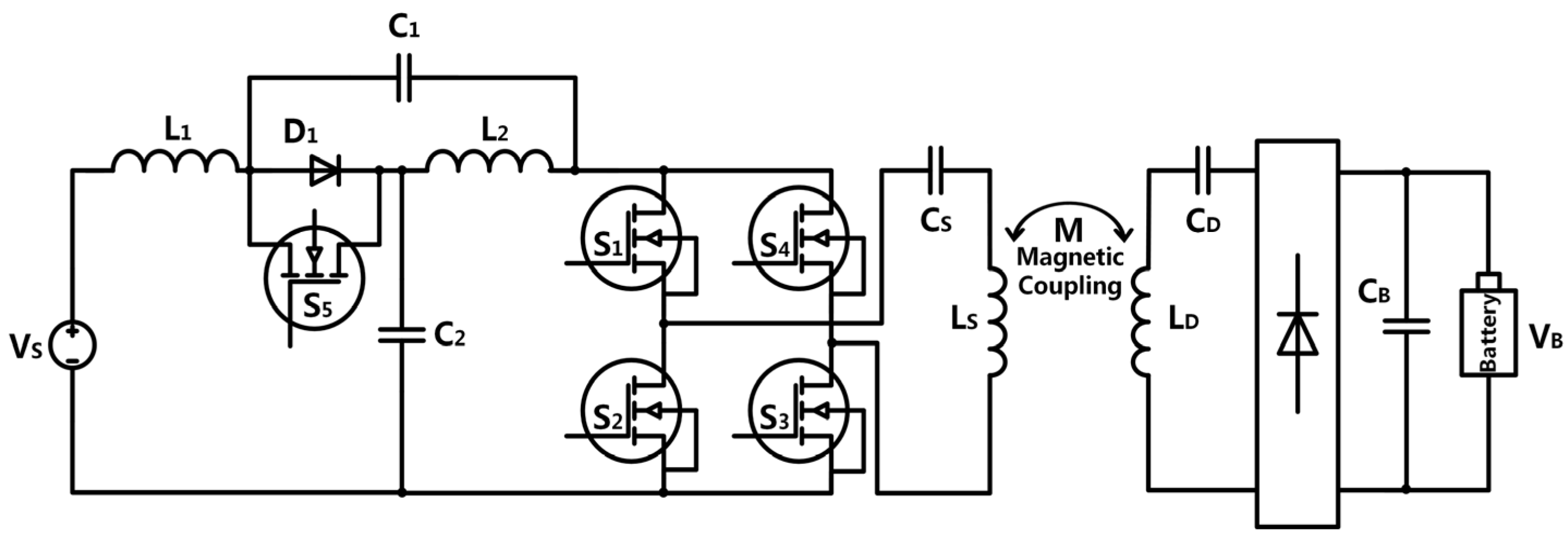
:1. Introduction
2. Comparative Analysis of Resonant Topologies
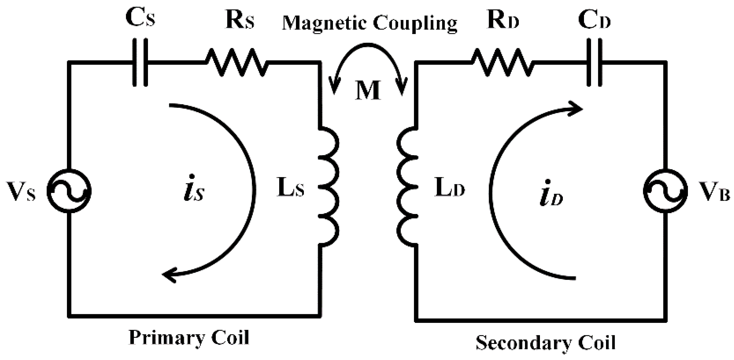
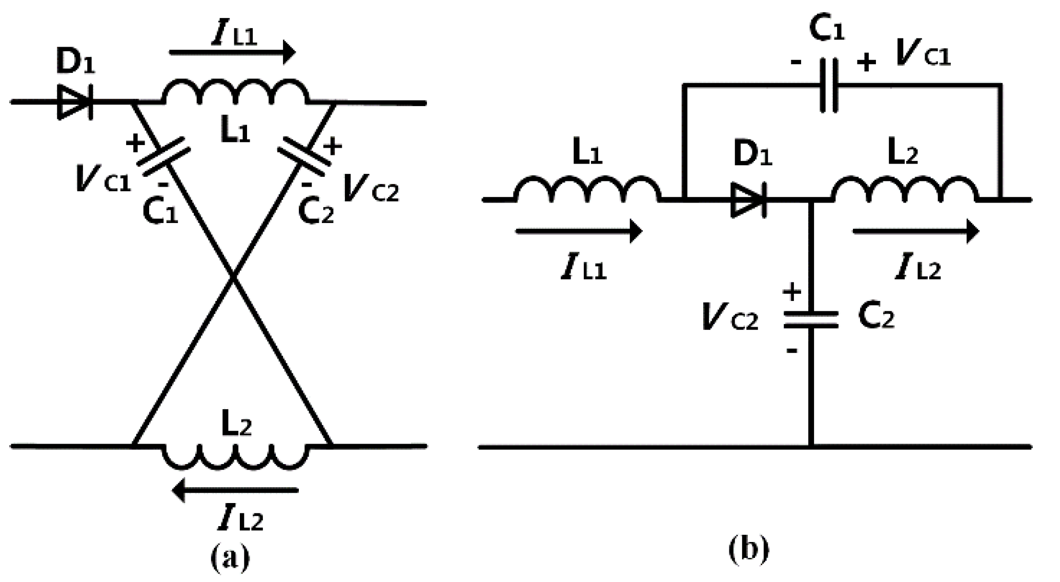
2.1. LC-LC Series Topology
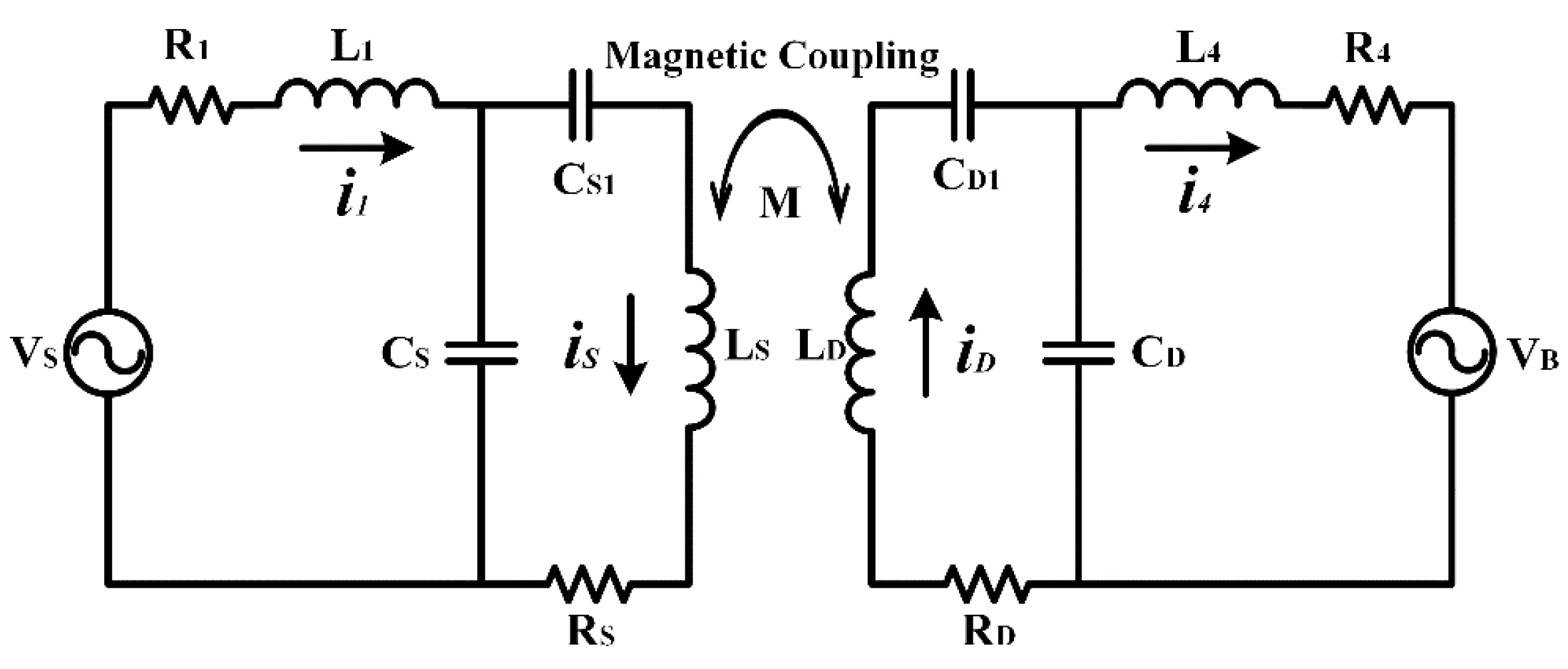
2.2. LCL-LCL Topology
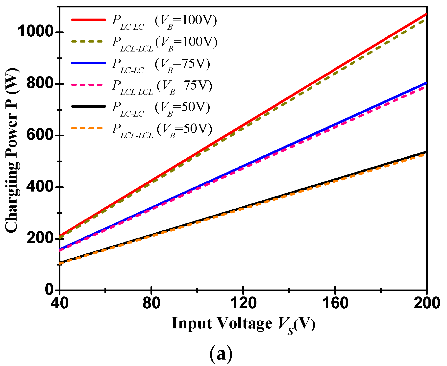
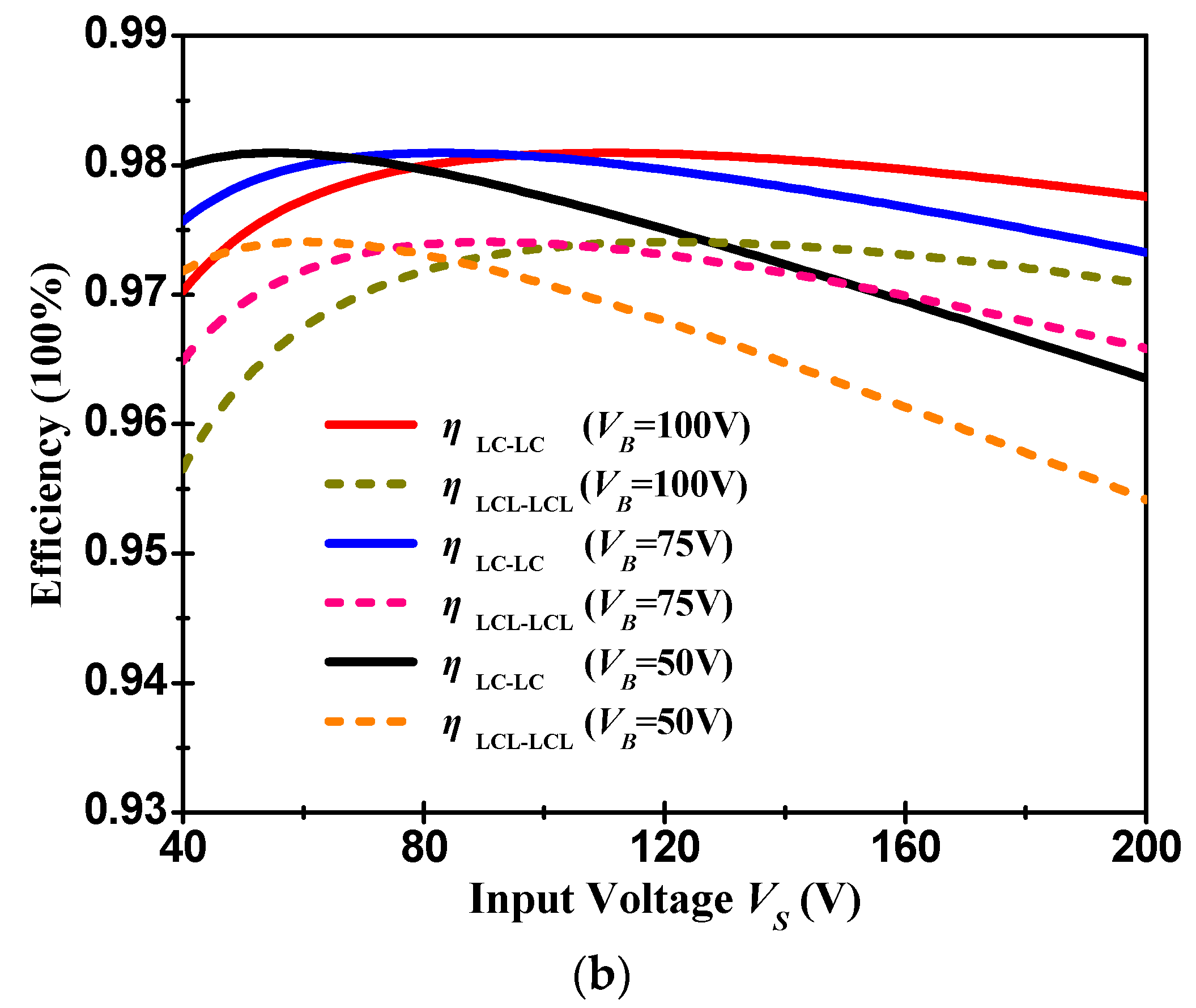
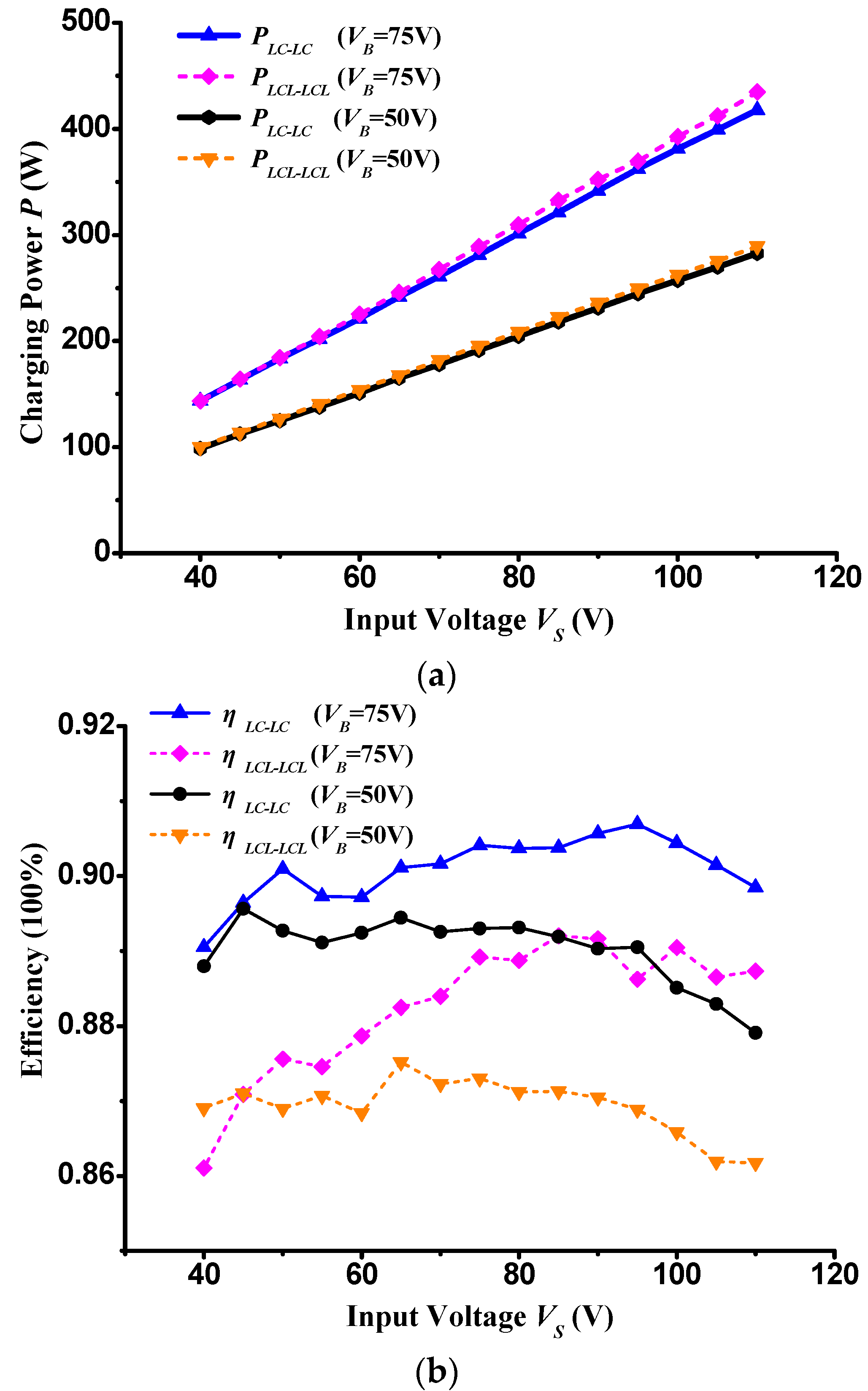
2.3. Comparison between the LC-LC Series Topology and LCL-LCL Topology

| LC-LC Series Topology | LCL-LCL Topology | ||
|---|---|---|---|
| Electric parameters | Value | Electric parameters | Value |
| Primary inductor LS | 290.18 μH | Compensating inductor L1 | 43.2 μH |
| Parasitic resistance RS | 193 mΩ | Parasitic resistance R1 | 53 mΩ |
| Primary capacitor CS | 34.83 nF | Primary resonant capacitor CS | 234.75 nF |
| Secondary inductor LD | 329.4 μH | Primary inductor LS | 290.18 μH |
| Parasitic resistance RD | 213 mΩ | Parasitic resistance RS | 193 mΩ |
| Secondary capacitor CD | 30.89 nF | Compensating capacitor CS1 | 40.68 nF |
| Secondary inductor LD | 329.4 μH | ||
| Parasitic resistance RD | 213 mΩ | ||
| Compensating capacitor CD1 | 35.07 nF | ||
| Compensating inductor L4 | 42.5 μH | ||
| Parasitic resistance R4 | 42.5 mΩ | ||
| Secondary resonant capacitor CD | 238.63 nF | ||


3. Online Power Regulation
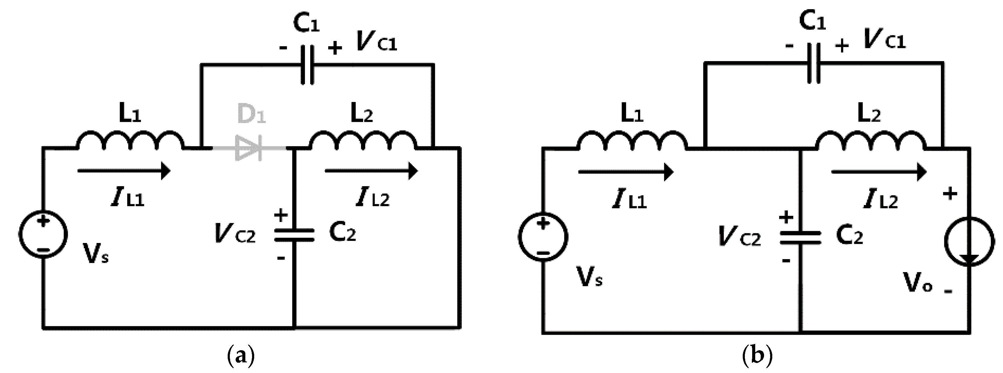
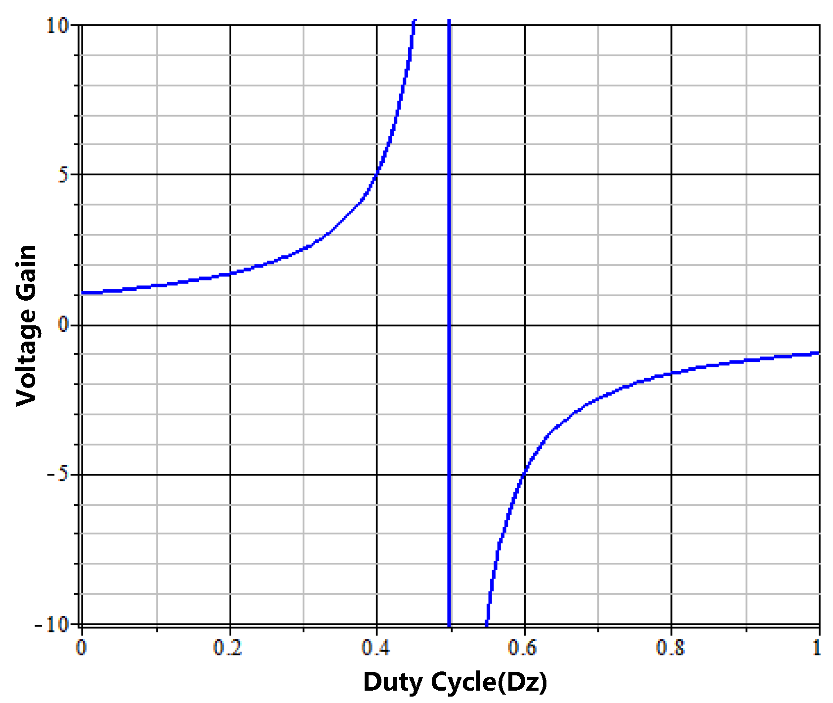
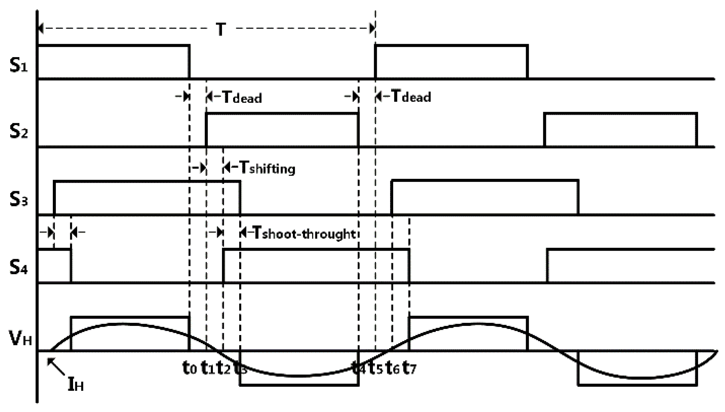
3.1. Principles of q-Zsource


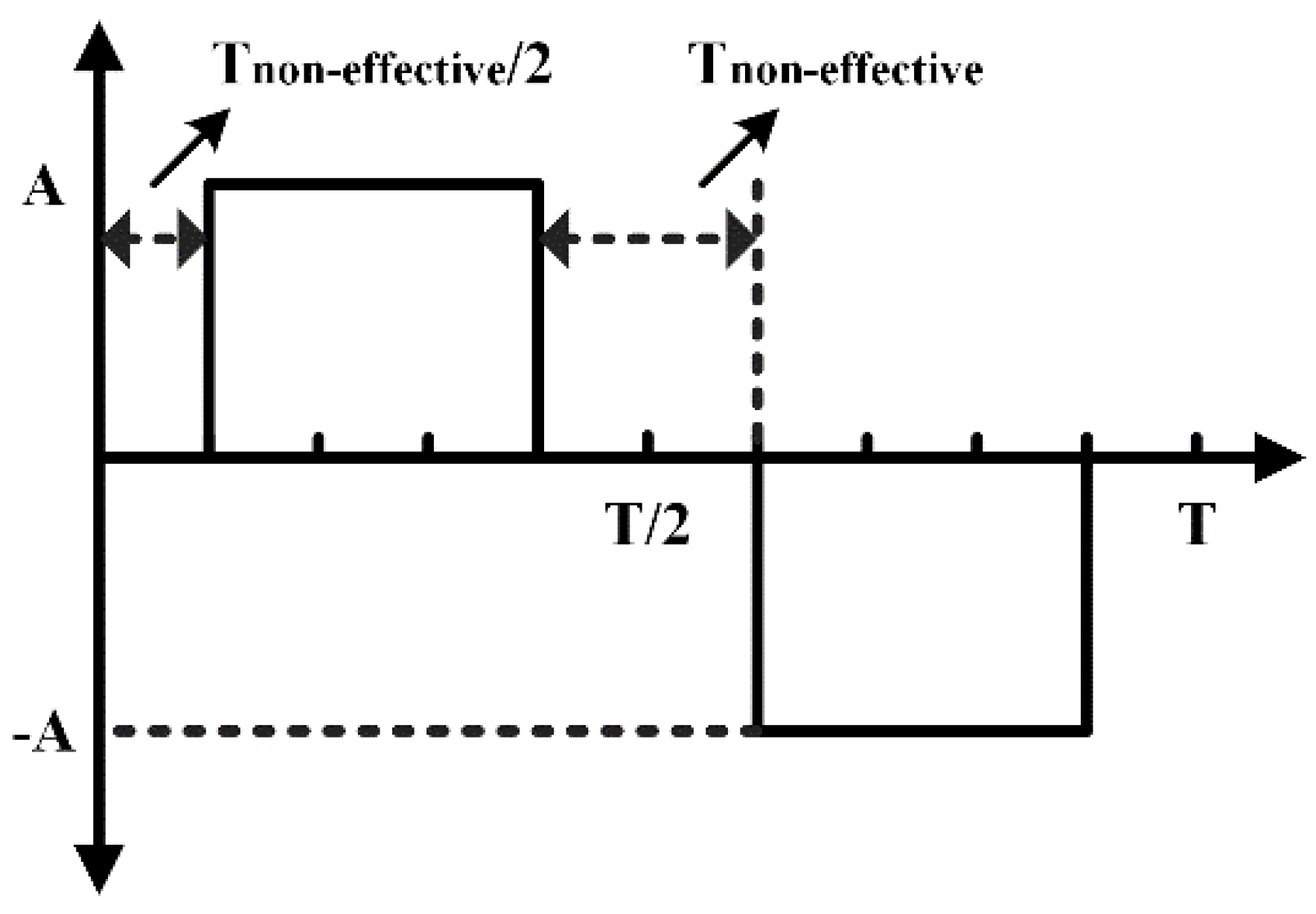
3.2. Control Method

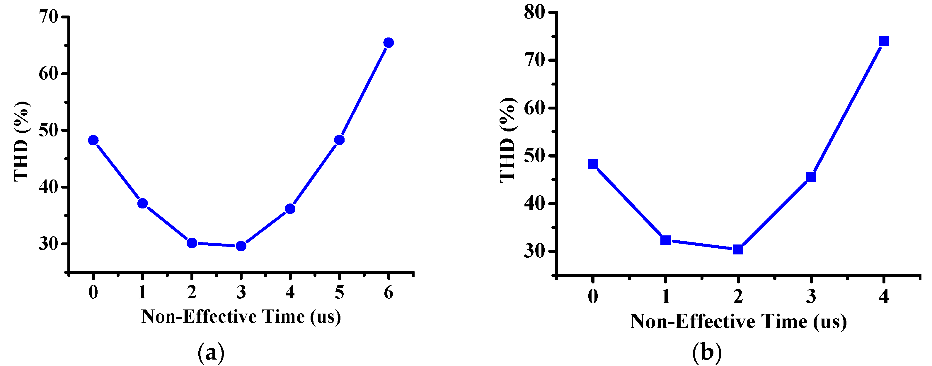
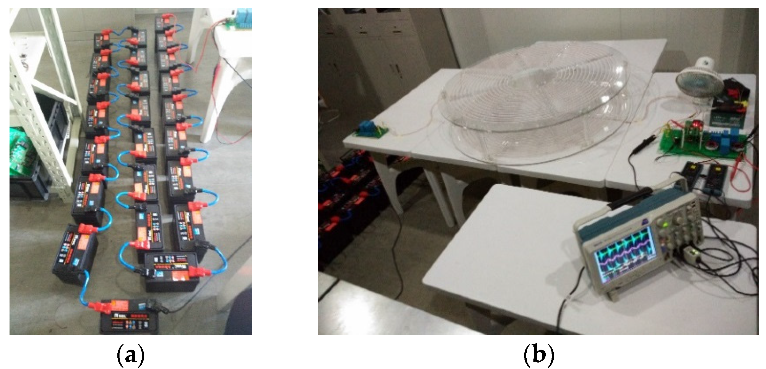
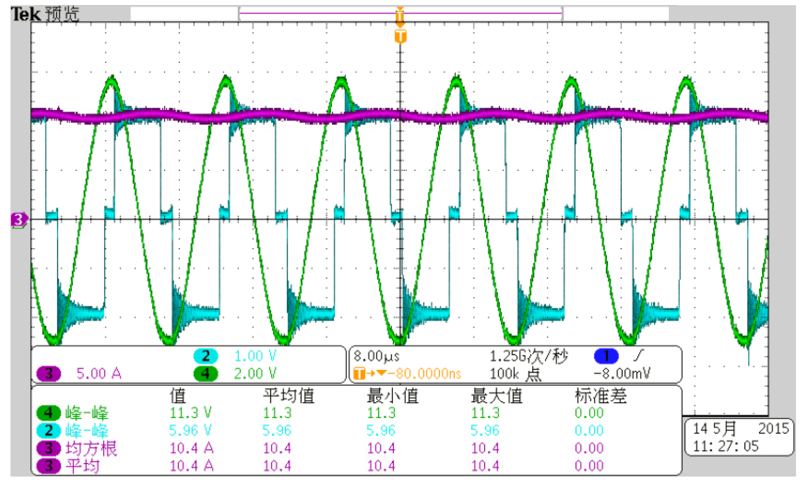
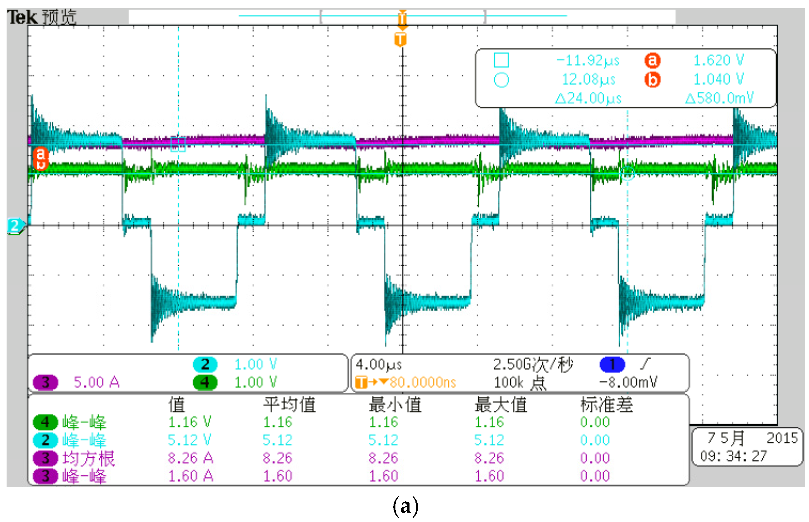
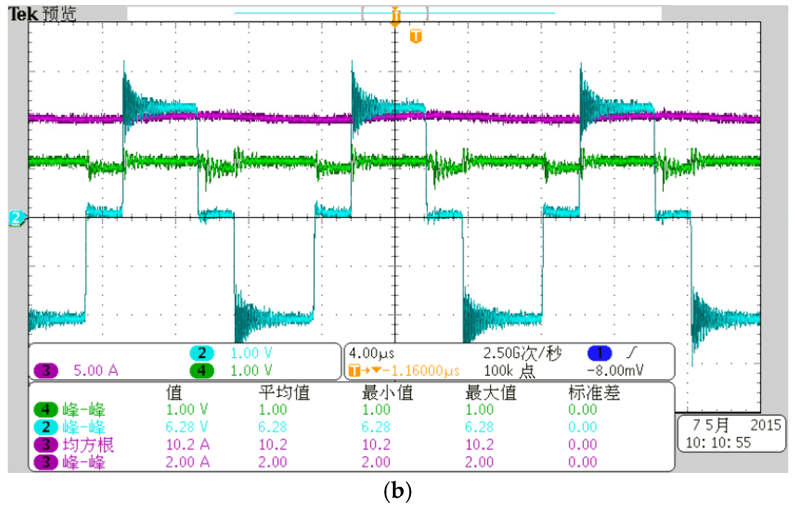
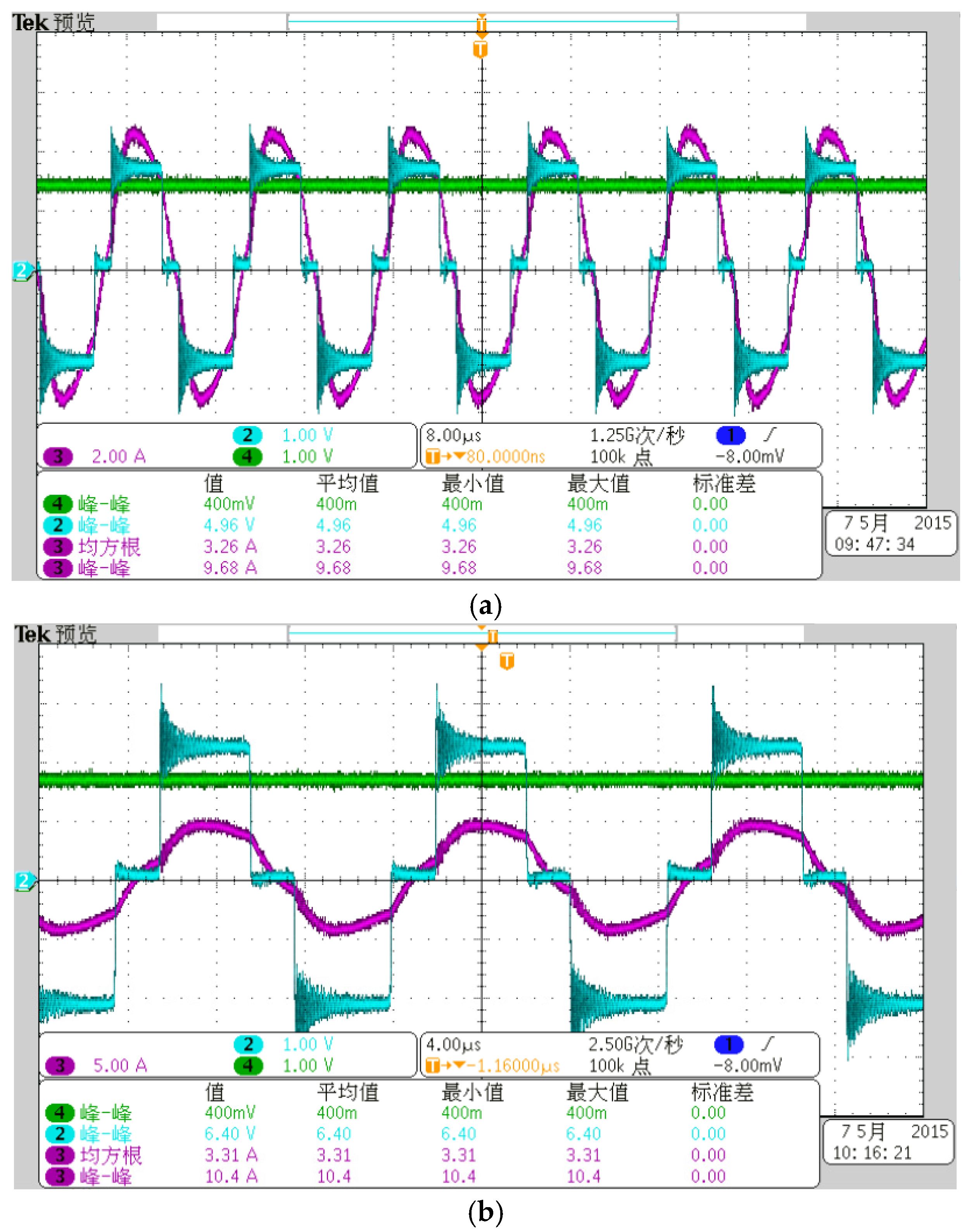
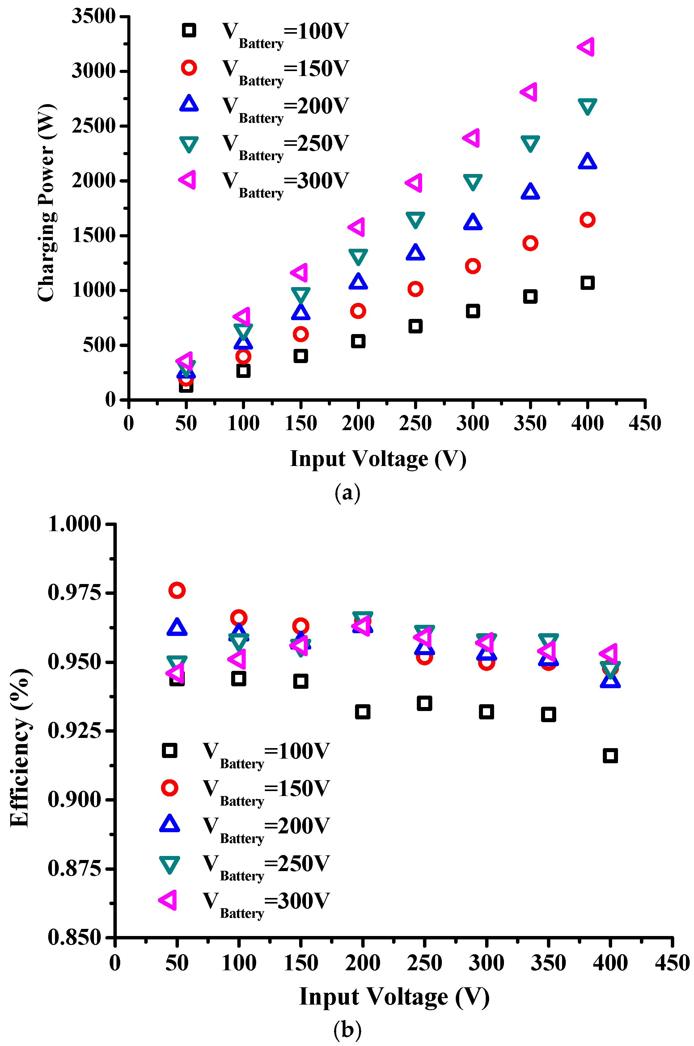
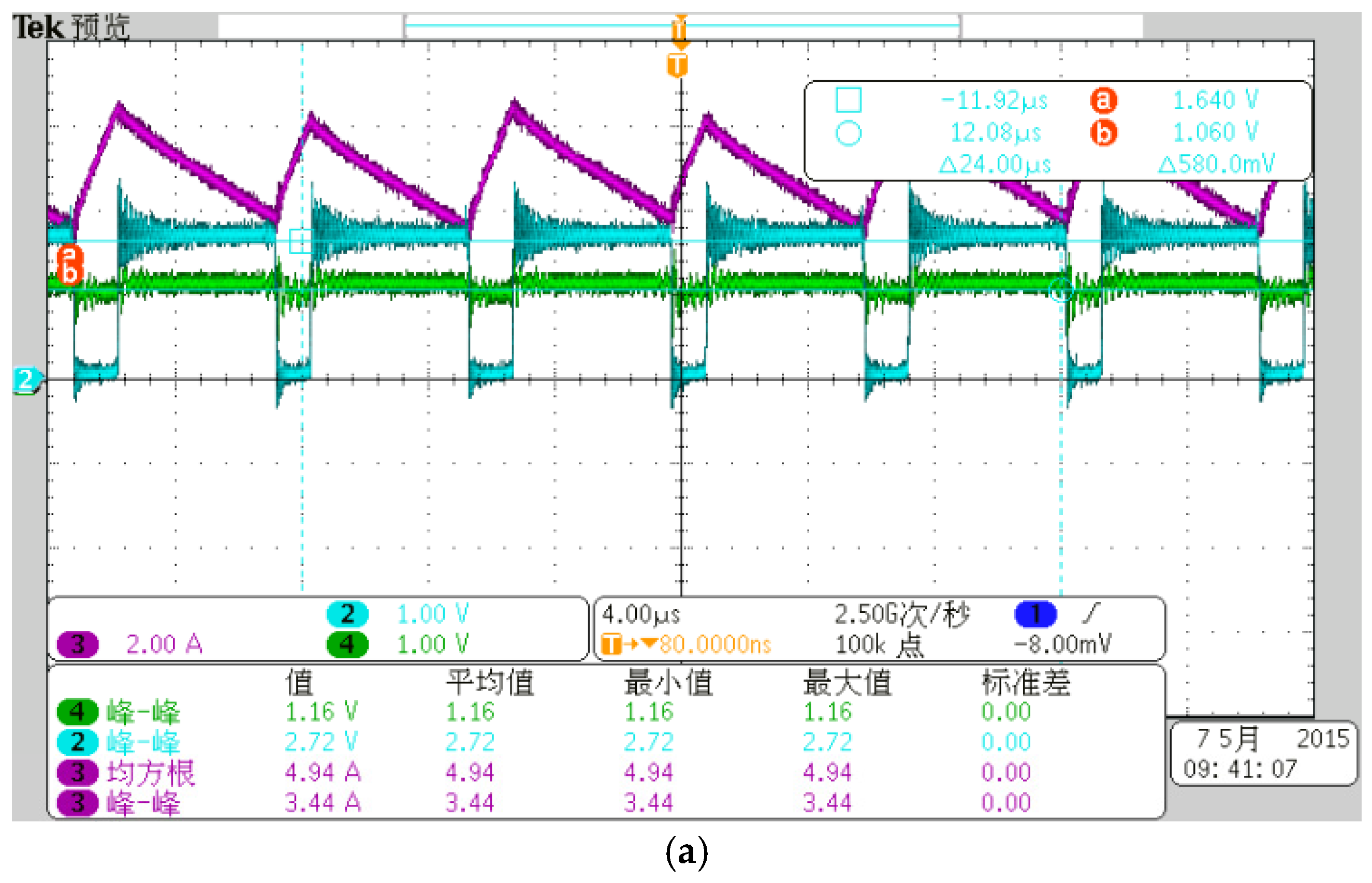
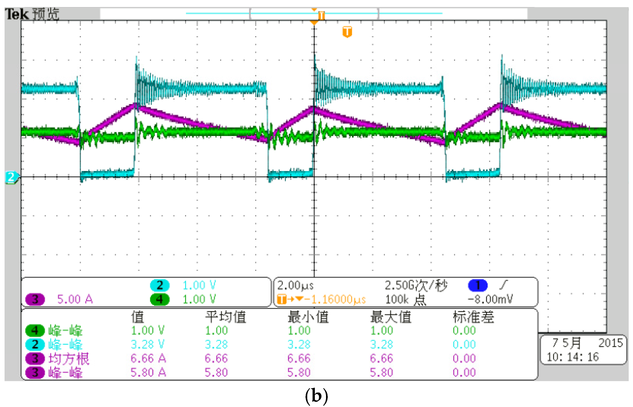
4. Experiments


5. Conclusions
Acknowledgments
Author Contributions
Conflicts of Interest
References
- Brown, W.C. The history of power transmission by radio waves. IEEE Trans. Microwave Theory Tech. 1984, 32, 1230–1242. [Google Scholar] [CrossRef]
- Tucker, C.A.; Warwick, K.; Holderbaum, W. A contribution to the wireless transmission of power. Int. J. Electr. Power Energy Syst. 2013, 47, 235–242. [Google Scholar] [CrossRef]
- Brown, W.C. Status of the microwave power transmission components for the solar power satellite (SPS). IEEE MTT-S Int. Microwave Symp. Dig. 1981, 81, 270–272. [Google Scholar]
- Glaser, P.E. Power from the Sun: Its future. Science 1968, 162, 857–861. [Google Scholar] [CrossRef] [PubMed]
- Covic, G.A.; Boys, J.T. Modern trends in inductive power transfer for transportation applications. IEEE J. Emerg. Sel. Top. Power Electr. 2013, 1, 28–41. [Google Scholar] [CrossRef]
- Wei, X.Z.; Wang, Z.S.; Dai, H.F. A critical review of wireless power transfer via strongly coupled magnetic resonances. Energies 2014, 7, 4316–4341. [Google Scholar] [CrossRef]
- Kurs, A.; Karalis, A.; Moffatt, R.; Joannopoulos, J.D.; Fisher, P.; Soljacic, M. Wireless power transfer via strongly coupled magnetic resonances. Science 2007, 317, 83–86. [Google Scholar] [CrossRef] [PubMed]
- Sample, A.P.; Meyer, D.A.; Smith, J.R. Analysis, experimental results, and range adaptation of magnetically coupled resonators for wireless power transfer. IEEE Trans. Ind. Electron. 2011, 58, 544–554. [Google Scholar] [CrossRef]
- Li, X.H.; Zhang, H.R.; Peng, F.; Li, Y.; Yang, T.Y.; Wang, B.; Fang, D. A wireless magnetic resonance energy transfer system for micro implantable medical sensors. Sensors 2012, 12, 10292–10308. [Google Scholar] [CrossRef] [PubMed]
- Puccetti, G.; Stevens, C.J.; Reggiani, U.; Sandrolini, L. Experimental and numerical investigation of termination impedance effects in wireless power transfer via metamaterial. Energies 2015, 8, 1882–1895. [Google Scholar] [CrossRef]
- Sun, L.; Tang, H.; Zhang, Y. Determining the frequency for load-independent output current in three-coil wireless power transfer system. Energies 2015, 8, 9719–9730. [Google Scholar] [CrossRef]
- Sanghoon, C.; Yong-Hae, K.; Kang, S.-Y.; Myung-Lae, L.; Jong-Moo, L.; Zyung, T. Circuit-model-based analysis of a wireless energy-transfer system via coupled magnetic resonances. IEEE Trans. Ind. Electron. 2011, 58, 2906–2914. [Google Scholar]
- Kiani, M.; Uei-Ming, J.; Ghovanloo, M. Design and optimization of a 3-coil inductive link for efficient wireless power transmission. IEEE Trans. Biomed. Circuits Syst. 2011, 5, 579–591. [Google Scholar] [CrossRef] [PubMed]
- Dukju, A.; Songcheol, H. A study on magnetic field repeater in wireless power transfer. IEEE Trans. Ind. Electron. 2013, 60, 360–371. [Google Scholar]
- Musavi, F.; Eberle, W. Overview of wireless power transfer technologies for electric vehicle battery charging. IET Power Electron. 2014, 7, 60–66. [Google Scholar] [CrossRef]
- Del Toro, T.G.X.; Vázquez, J.; Roncero-Sanchez, P. Design, implementation issues and performance of an inductive power transfer system for electric vehicle chargers with series-series compensation. IET Power Electron. 2015, 8, 1920–1930. [Google Scholar]
- Siqi, L.; Mi, C.C. Wireless power transfer for electric vehicle applications. IEEE J. Emerg. Sel. Top. Power Electron. 2015, 3, 4–17. [Google Scholar] [CrossRef]
- Keeling, N.A.; Covic, G.A.; Boys, J.T. A unity-power-factor IPT pickup for high-power applications. IEEE Trans. Ind. Electron. 2010, 57, 744–751. [Google Scholar] [CrossRef]
- Hwang, S.-H.; Kang, C.G.; Son, Y.-H.; Jang, B.-J. Software-based wireless power transfer platform for various power control experiments. Energies 2015, 8, 7677–7689. [Google Scholar] [CrossRef]
- Zaheer, A.; Covic, G.A.; Kacprzak, D. A bipolar pad in a 10-kHz 300-W distributed IPT system for AGV applications. IEEE Trans. Ind. Electron. 2014, 61, 3288–3301. [Google Scholar] [CrossRef]
- Madawala, U.K.; Thrimawithana, D.J. New technique for inductive power transfer using a single controller. IET Power Electron. 2012, 5, 248–256. [Google Scholar] [CrossRef]
- Gao, Y.; Farley, K.; Tse, Z. A uniform voltage gain control for alignment robustness in wireless EV charging. Energies 2015, 8, 8355–8370. [Google Scholar] [CrossRef]
- Chwei-Sen, W.; Covic, G.A.; Stielau, O.H. Power transfer capability and bifurcation phenomena of loosely coupled inductive power transfer systems. IEEE Trans. Ind. Electron. 2004, 51, 148–157. [Google Scholar]
- Ricketts, D.S.; Chabalko, M.J.; Hillenius, A. Experimental demonstration of the equivalence of inductive and strongly coupled magnetic resonance wireless power transfer. Appl. Phys. Lett. 2013, 102, 053904. [Google Scholar] [CrossRef]
- Birrell, S.A.; Wilson, D.; Yang, C.P.; Dhadyalla, G.; Jennings, P. How driver behaviour and parking alignment affects inductive charging systems for electric vehicles. Transp. Res. C Emerg. Technol. 2015, 58, 721–731. [Google Scholar] [CrossRef]
- Choi, W.P.; Ho, W.C.; Liu, X.; Hui, S.Y.R. Comparative study on power conversion methods for wireless battery charging platform. In Proceedings of the 2010 14th International Power Electronics and Motion Control Conference (EPE/PEMC), Ohrid, Macedonia, 6–8 September 2010; pp. S15:9–S15:16.
- Xuan, N.B.; Vilathgamuwa, D.M.; Foo, G.H.B.; Peng, W.; Ong, A.; Madawala, U.K.; Trong, D.N. An Efficiency Optimization Scheme for Bidirectional Inductive Power Transfer Systems. IEEE Trans. Power Electron. 2015, 30, 6310–6319. [Google Scholar]
- Jun-Young, L.; Byung-Moon, H. A Bidirectional Wireless Power Transfer EV Charger Using Self-Resonant PWM. IEEE Trans. Power Electron. 2015, 30, 1784–1787. [Google Scholar]
- Madawala, U.K.; Thrimawithana, D.J. A Bidirectional Inductive Power Interface for Electric Vehicles in V2G Systems. IEEE Trans. Ind. Electron. 2011, 58, 4789–4796. [Google Scholar] [CrossRef]
- Madawala, U.K.; Thrimawithana, D.J. Modular-based inductive power transfer system for high-power applications. IET Power Electron. 2012, 5, 1119–1126. [Google Scholar] [CrossRef]
- Xuan, N.B.; Foo, G.; Ong, A.; Vilathgamuwa, D.M.; Madawala, U.K. Efficiency optimization for bidirectional IPT system. In Proceedings of the 2014 IEEE Transportation Electrification Conference and Expo (ITEC), Dearborn, MI, USA, 15–18 June 2014; pp. 1–5.
- Madawala, U.K.; Thrimawithana, D.J. Current sourced bi-directional inductive power transfer system. IET Power Electron. 2011, 4, 471–480. [Google Scholar] [CrossRef]
- Zheng, P.F. Z-source inverter. IEEE Trans.Ind. Appl. 2003, 39, 504–510. [Google Scholar] [CrossRef]
- Peng, F.X.; Guang, W.X.; Qiao, C.Z. A single-phase AC power supply based on modified Quasi-Z-Source Inverter. IEEE Trans. Appl. Supercond. 2014, 24, 1–5. [Google Scholar] [CrossRef]
- Boys, J.T.; Covic, G.A. Decoupling Circuits. U.S. 7279850B2, 9 October 2005. [Google Scholar]
- Hothongkham, P.; Kongkachat, S.; Thodsaporn, N. Performance comparison of PWM and phase-shifted PWM inverter fed high-voltage high-frequency ozone generator. In Proceedings of the 2011 IEEE Region 10 Conference on Convergent Technologies for the Asia-Pacific Region, Bali, Indonesia, 21–24 November 2011; pp. 976–980.
© 2015 by the authors; licensee MDPI, Basel, Switzerland. This article is an open access article distributed under the terms and conditions of the Creative Commons by Attribution (CC-BY) license (http://creativecommons.org/licenses/by/4.0/).
Share and Cite
Wang, Z.; Wei, X.; Dai, H. Design and Control of a 3 kW Wireless Power Transfer System for Electric Vehicles. Energies 2016, 9, 10. https://doi.org/10.3390/en9010010
Wang Z, Wei X, Dai H. Design and Control of a 3 kW Wireless Power Transfer System for Electric Vehicles. Energies. 2016; 9(1):10. https://doi.org/10.3390/en9010010
Chicago/Turabian StyleWang, Zhenshi, Xuezhe Wei, and Haifeng Dai. 2016. "Design and Control of a 3 kW Wireless Power Transfer System for Electric Vehicles" Energies 9, no. 1: 10. https://doi.org/10.3390/en9010010
APA StyleWang, Z., Wei, X., & Dai, H. (2016). Design and Control of a 3 kW Wireless Power Transfer System for Electric Vehicles. Energies, 9(1), 10. https://doi.org/10.3390/en9010010