1. Introduction
The world has witnessed a rapid growth of plug-in hybrid electric vehicles (PHEVs) and pure electric vehicles (EVs) over the past decade due to the increase in greenhouse gas emissions, environmental pollutants, and fossil-fuel price fluctuations. However, PHEVs and EVs still need to address range anxiety, high battery cost, and the inconvenience of charging before their widespread acceptance [
1,
2]. Wireless power transfer (WPT) has been an emerging research area for several years and could overcome the inconvenience of EV charging [
1]. WPT allows power to transfer from a transmitter coil to a receiver coil over an air gap. Applications for WPT include mobile devices, household facilities, medical implants, and electric vehicles [
1,
2,
3,
4,
5,
6,
7]. WPT is based on the principle of magnetic resonance couplings. The WPT system is mainly composed of a high-frequency power inverter, transmitter coil (also called “primary side”), receiver coil (also called “secondary side”), compensation capacitors, and rectification electronics. The alternating magnetic field generated by the primary side induces an alternating current in the secondary side. The rectifier converts the alternating current into direct current (DC), and then a DC-DC converter can be used to drive the desired load—for example, a battery. The compensation capacitors make up for the large inductance leakage and allow for a loose coupling, so power can transfer wirelessly across a large air gap.
WPT systems are frequency-sensitive due to their use of magnetic resonance. Any change in the resonant components, such as inductance, capacitance or load, can influence the operating frequency of the system. Since WPT systems operate in a non-contact manner, the physical spacing between the two coils can vary, resulting in a change in magnetic coupling and eventually shifting the best switching frequency for WPT [
8]. Often, EVs used in everyday life are not parked in the ideal position over the transmitter each time. The misalignment between the two coils influences the output voltage at the secondary side and hence changes the power delivery. Additionally, the chassis height might be different for different EVs, which can also influence the optimal switching frequency.
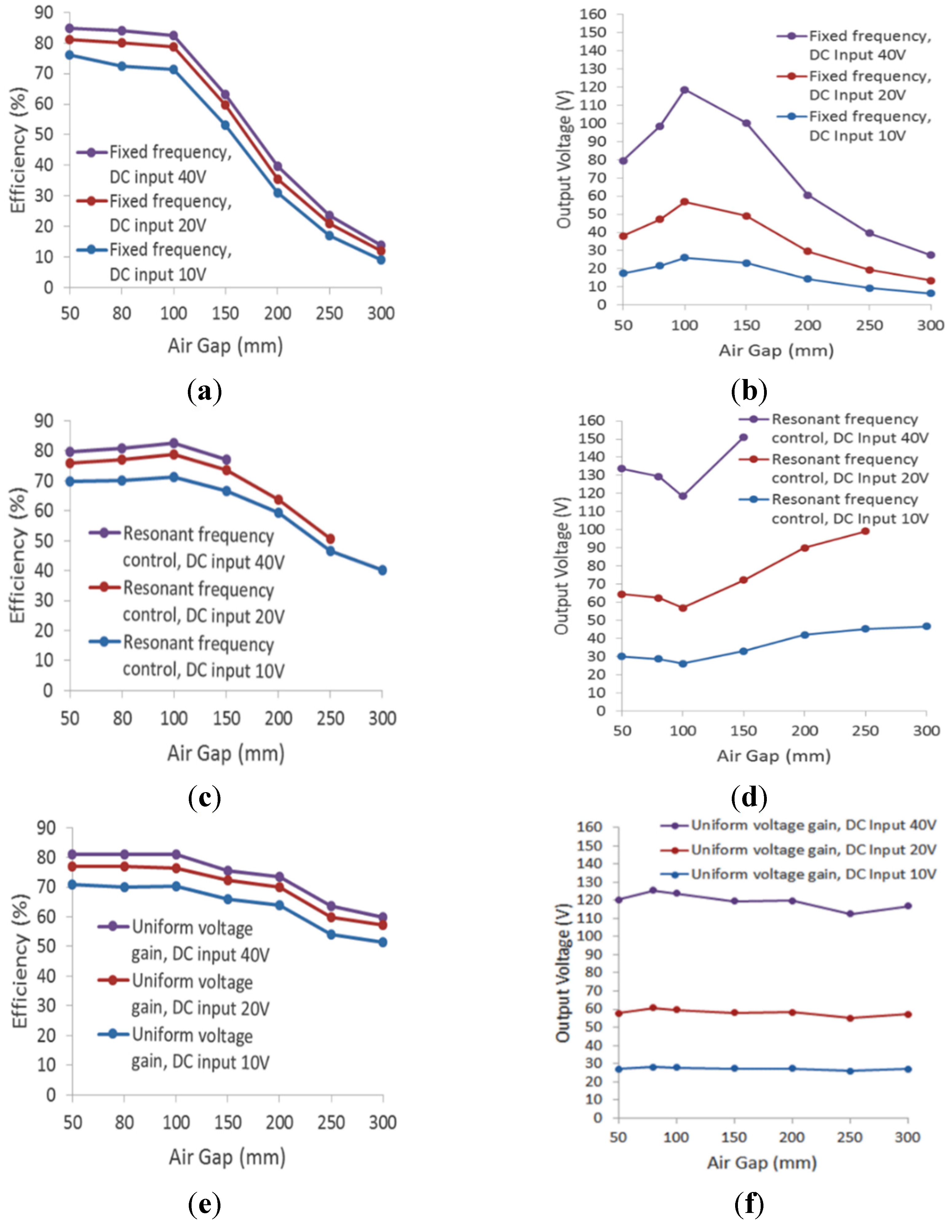
The body of this study focuses on a uniform voltage gain control method to address the frequency shift caused by misalignment and different air gaps while keeping the output voltage stable. A WPT system was developed to experimentally demonstrate the proposed frequency control under different coil alignments. There are four common resonant tank topologies for WPT based on different capacitor arrangements, including series-series (SS), series-parallel (SP), parallel-series (PS), and parallel-parallel (PP). A popular SP resonant tank is used as an example to demonstrate the frequency control in the experiment.
The WPT frequency controls fall into two categories: fixed frequency control and variable frequency control (also called “adaptive frequency control”). A fixed frequency control is normally operated under limited magnetic coupling variances, and a typical input voltage control is used to keep the charging voltage constant [
9]. Resonant frequency control, which is a kind of variable frequency control, is designed to improve the WPT’s adaptability for coupling change. Resonant frequency control allows WPT to always operate at a zero phase angle between the output voltage and current in the primary inverters. However, this causes the circulating current for resonant control to be quite high. In some studies, soft switching techniques are used to minimize the power losses of switching devices where the phase angle is forced to shift to a small value, making the WPT under-coupled [
1,
8,
10,
11,
12]. There are several different ways to provide resonant frequency control, such as adding auxiliary components to adapt to the variance of magnetic couplings and directly switching the frequency of gate signals. For example, Aldhaher
et al. adjusted the operating frequency by using saturable reactors [
13], and the WPT system developed by Han
et al. can adjust a different resonant capacitor and then change the operating frequency [
14]. Although these auxiliary resonant components help to switch the frequency indirectly, they increase the cost of wireless chargers, especially in high power applications, and the additional electronic elements make the WPT system bulky. An automatic frequency tuning system is proposed by Sample
et al. and Kar
et al., where the WPT is tuned and operated at its resonant frequency, resulting in a zero load phase angle [
8,
15]. Although the system is physically resonant, the output voltage at the secondary side is varied under different coil spacing, making it difficult to regulate power delivery to the battery. To address the influence of load variances on output voltage, a universal WPT was designed to charge different batteries [
11,
16]. However, the universal system did not compensate for misalignment issues. Moreover, a different hardware configuration was used to achieve variable frequency control for WPT. Most of the proposed variable frequency controllers calculate the voltage and current of the secondary side via wireless communications, which can increase the cost and overall system complexity.
Wireless charging systems could operate at an adaptive switching frequency with uniform voltage gain in order to compensate for misalignment. The frequency control proposed in this paper is based on voltage gain and impedance analysis across the frequency domain, and the uniform voltage gain control is achieved through phase angle feedback at the primary side.
3. Phase Angle Measurement
The phase angle between the primary inverter’s output current and voltage can be used to calculate the WPT’s frequency. The operating frequency influences both the voltage gain and the phase angle. Thus, the phase angle must be measured in order to find and adjust the operating frequency to control the WPT system’s power delivery.
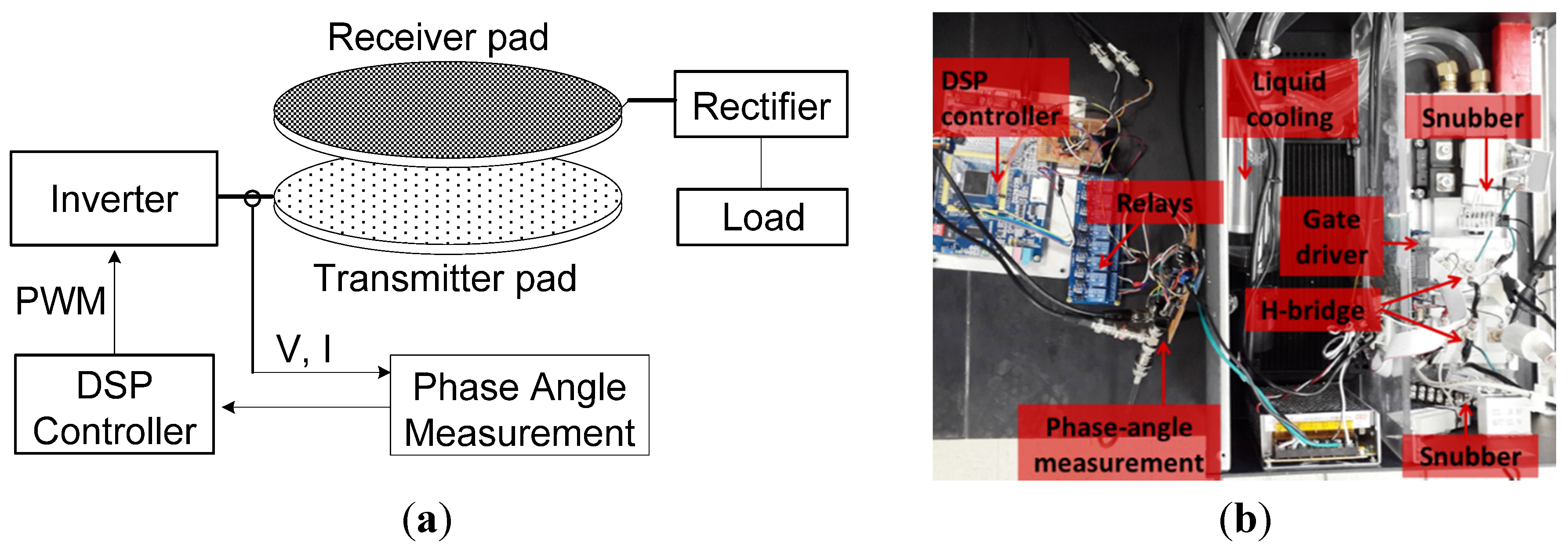
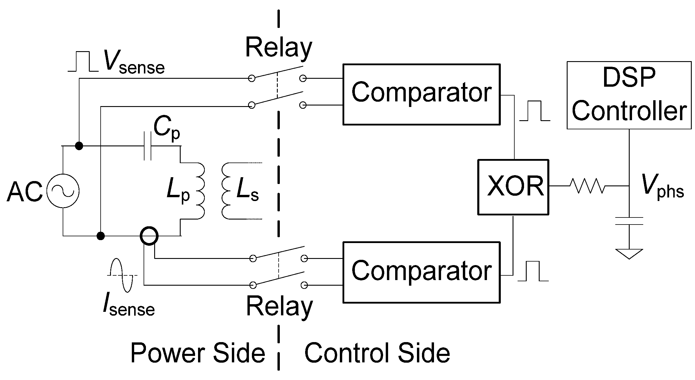
Figure 2 shows the schematic design of the phase angle measurement circuit. The output voltage (
Vsense) and current (
Isense) signals from the power inverter (modeled as an AC source in
Figure 2) are transformed into two square waveforms by comparators. An exclusive-OR gate (XOR) combines the two square waveforms to one pulse waveform whose width is equal to the phase delay between
Vsense and
Isense. A low-pass filter converts the pulse into a DC signal
Vphs, which can be acquired by the analog-to-digital converter (ADC) in the DSP controller. The DC output of the filter is proportional to the phase angle between
Vsense and
Isense. Since the high power in the WPT system can destroy the comparators and control circuit, four relays were used to isolate the power and control sides, as shown in
Figure 2.
Figure 2.
Schematic of phase angle measurement.
Figure 2.
Schematic of phase angle measurement.
Because the switching frequency is greater than 10 kHz, and at times even 100 kHz, it is quite difficult for a commercialized hall-effect voltage sensor to pick up the high speed. The voltage probe is directly connected to the output of the power inverter and then to the comparator. A current transformer is used to measure the circulating current in the coil. Although discrete Fourier transform (DFT) can be programmed in the DSP for phase angle measurements, using an XOR and an RC filter greatly simplifies the embedded software development process and reduces the computational load of the DSP.
Once the phase angle has been measured, the switching frequency must be adjusted until uniform voltage gain is achieved. The DC input voltage is limited to 12 V during the frequency tuning process because lower voltage levels are much safer for the control circuit, and frequency tuning at high power levels would prolong the tuning time. Additionally, unreasonably fast variance of the frequency generates instability of output voltage and power emissions in high-power applications, which could damage the battery. Hence, frequency tuning is designed to occur at low power levels for both tuning speed and the safety of the circuit. After the switching frequency is well tuned, the WPT system operates at high power and starts charging.
4. Analysis and Simulation of WPT
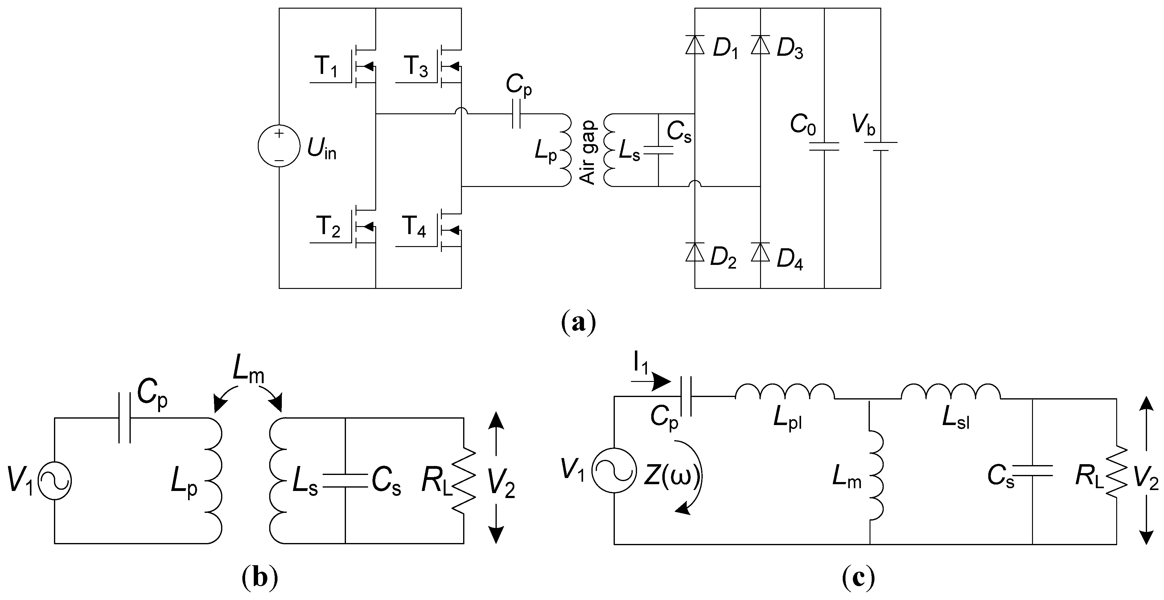
A full-bridge series-parallel WPT schematic is shown in
Figure 3a. The four semi-conductors were driven by square waveform signals with a duty cycle close to but less than 50% to avoid make-before-break situations (momentary short circuit) in the inverter. Although the energy consumption of the rectifier can lower the system efficiency due to the inherent voltage drop, its simplicity makes it an ideal choice for industrial use where reliability and low cost are highly valued.
Figure 3b is a simplified series-parallel circuit diagram, and
Figure 3c is the corresponding equivalent circuit. Equation (1) describes the circuit impedance (
Z) in terms of the switching frequency (
ω).
where
Cp is the series tuning capacitance of the primary side and
Cs is the tuning capacitance of the secondary side.
Cp must equal
Cs to achieve resonance.
Lpl and
Lsl are the leakage inductances of each coil. Since both coils are the same,
Lpl equals
Lsl.
Lm is the mutual inductance. The leakage and mutual inductance can be experimentally measured. The battery is equivalent to a resistive load,
RL, which can be calculated using the delivered power and voltage across the battery. For a desired 1.4 kW/120 V battery charging condition,
RL is 20 Ω.
j is the imaginary unit.
The coupling coefficient k is defined as
The voltage gain
G is the ratio of output voltage
V2 over input voltage
V1 as shown in
Figure 3c and is determined by
Figure 3.
Circuit diagram of proposed WPT system: (a) SP topology for WPT; (b) Simplified SP topology; (c) Equivalent circuit of SP topology.
Figure 3.
Circuit diagram of proposed WPT system: (a) SP topology for WPT; (b) Simplified SP topology; (c) Equivalent circuit of SP topology.
The mutual inductance changes with different coil alignments, which can cause a shift in the best switching frequency for WPT.
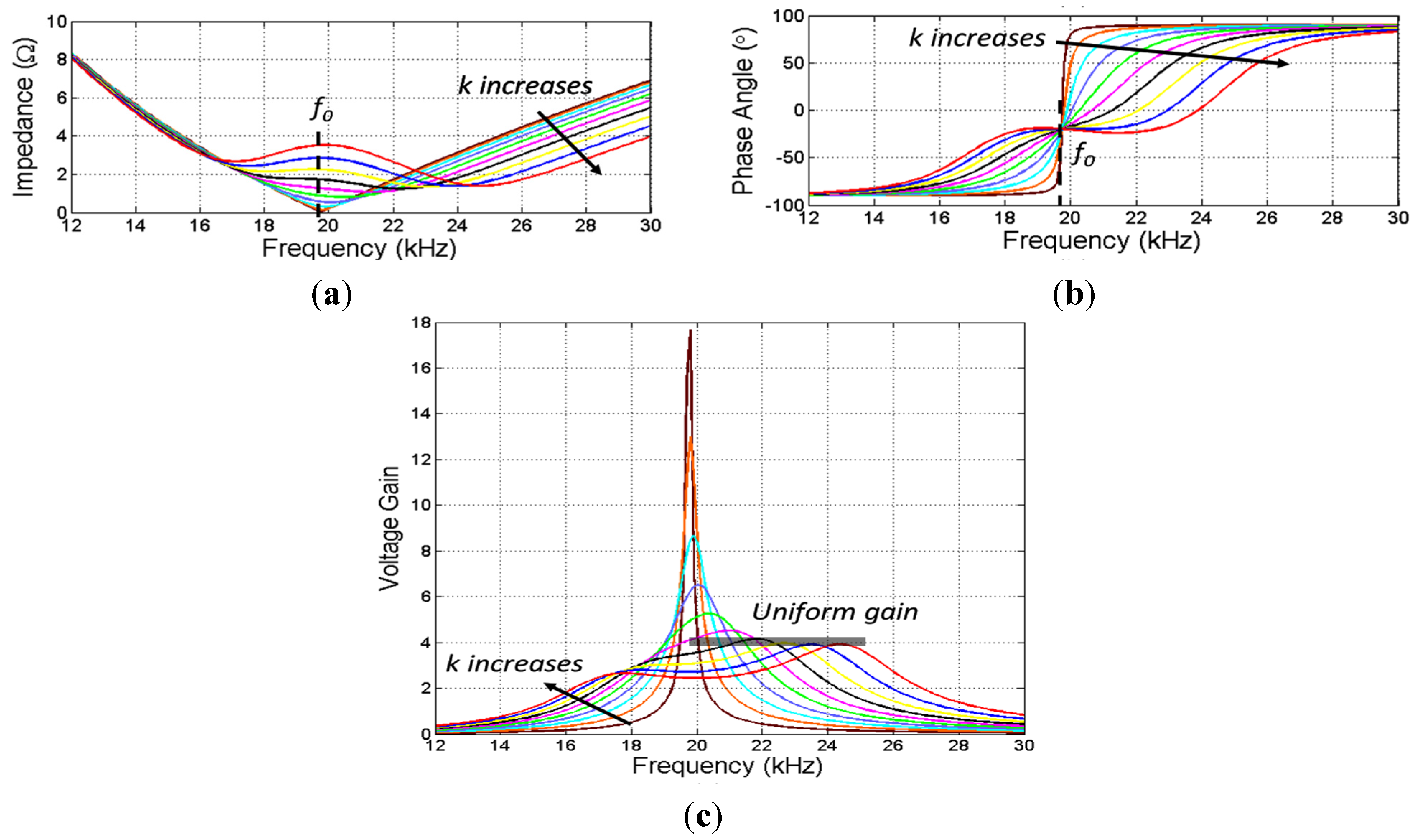
Figure 4 is a simulation result of impedance and voltage gain against frequency performed in Simulink (MathWorks, Natrick, MA, USA).
Figure 4a,b show that the resonant frequency of WPT varies due to different magnetic couplings.
Figure 4c is the voltage gain curve in the frequency domain. Although the WPT system has purely resistive impedance if operating at the resonant frequency, the voltage gain can change dramatically with different couplings, meaning that misalignment can cause the voltage output and power delivery to be unstable. The output voltage at resonance can be extremely high even under a weak coupling.
Although voltage gain varies at a specific frequency according to different magnetic couplings, uniform voltage gain can be achieved for a given coupling by changing the switching frequency. In
Figure 4b, each curve goes through one fixed phase angle value at frequency
f0. The phase angle is fixed at
f0 no matter how the coupling varies, but the voltage gain
G and impedance magnitude are the most unstable at
f0, so the WPT system cannot operate at
f0. On the left side of
f0, uniform gain theoretically exists, but the corresponding phase angle is much lower than on the right side of
f0, showing that the overall efficiency will be low if the WPT system operates on the left side of
f0. Therefore, the frequency range marked in
Figure 4c, on the right side of
f0, is seen as the uniform gain control area. In
Figure 4c, the frequency range for uniform gain control decreases from 24.4 kHz to 20.2 kHz when the coupling becomes weaker, and the corresponding phase angle is 18° at 24.4 kHz and 90° at 20.2 kHz. The total impedance is inductive in this frequency domain where the input voltage leads the input current, which realizes zero-voltage switching (ZVS) operation of the inverter.
Figure 4.
Impedance and voltage gain G in frequency domain. (a) Impedance magnitude; (b) Impedance phase characteristics; (c) Voltage gain in frequency domain. The simulation conditions were Lp = 65 μH, Ls = 65 μH, Cp = 1 μF, Cs = 1 μF, R = 20 Ω, and Lm = 2.5, 5, 7.5, 10, 12.5, 15, 17.5, 20, 22.5, and 25 μH.
For each curve of the phase angle in
Figure 4b, one zero-crossing point exists, which indicates the resonant frequency point. Therefore, the switching frequency can be shifted to some value higher than the resonant frequency in order to achieve uniform voltage gain by first detecting the phase angle. Since the phase angle measurement cannot detect polarity of angles, the first step is to find the resonant frequency, and then increase the frequency until the predetermined uniform gain is obtained. From
Figure 4b,c the phase angle for a uniform voltage gain is around 18°–22° as long as the magnetic coupling (
k) is relatively strong. The phase angle corresponding to the uniform voltage gain increases when the magnetic coupling becomes worse.
5. Control Loop Design
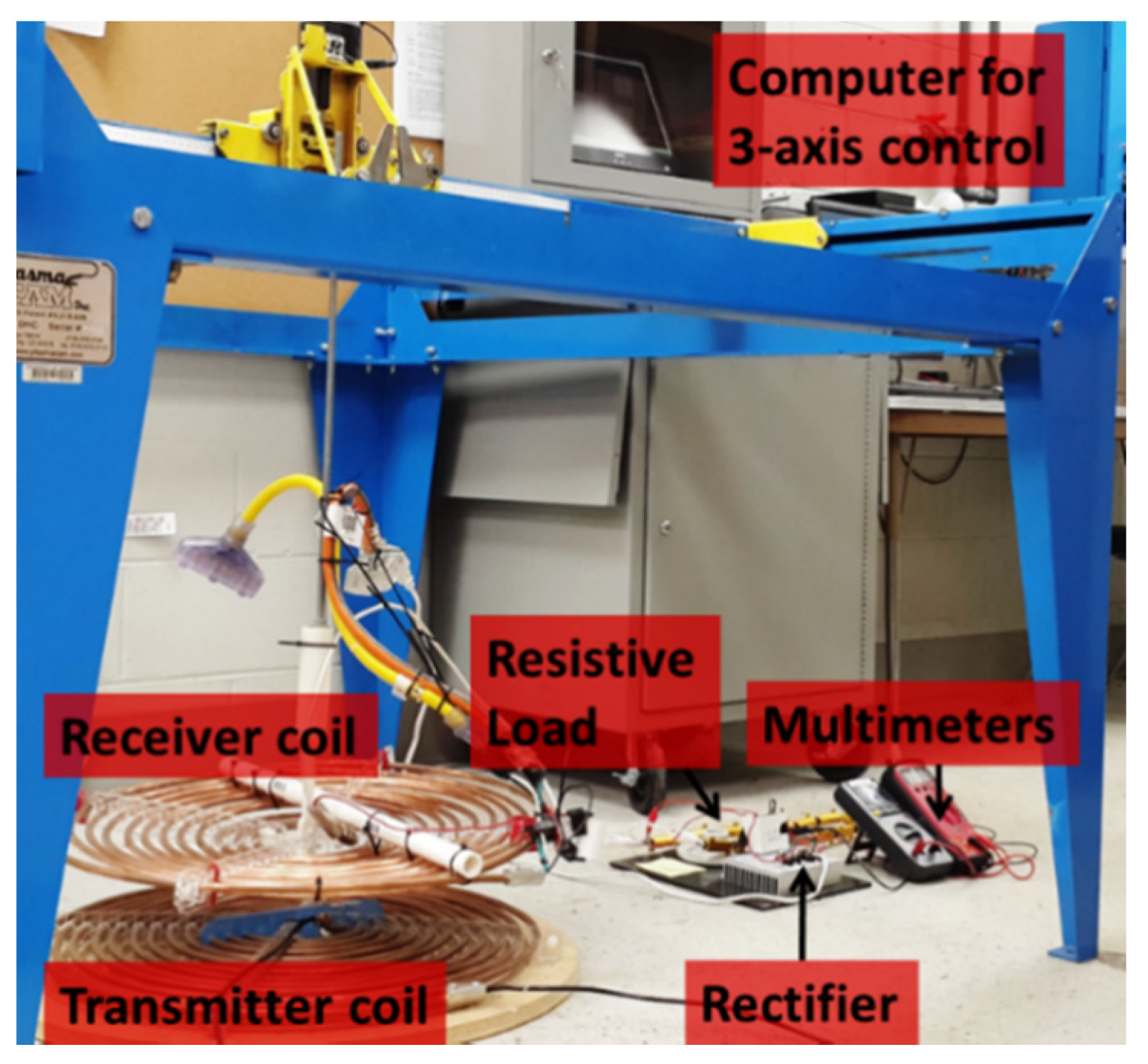
The main objective of this section is to explore the use of the proposed uniform gain control to generate a fixed output voltage regardless of any coil misalignment. The WPT is designed to automatically choose the optimal frequency after the EV is parked but before charging begins. A dummy resistor is required to simulate the battery status, as its equivalent resistive load can vary at different levels of charge.
The resonant frequency is the frequency that makes the load phase angle between the primary inverter’s input voltage and current zero. While the resonant frequency allows the system to transfer maximum power, the output voltage at the secondary side varies significantly, thus increasing the difficulty in designing a DC-DC converter that can ensure the charger voltage is stable. The non-zero phase angle between the primary inverter’s output voltage and current allows for the use of soft switches, decreasing the power losses caused by switching devices. The tuning process is as follows:
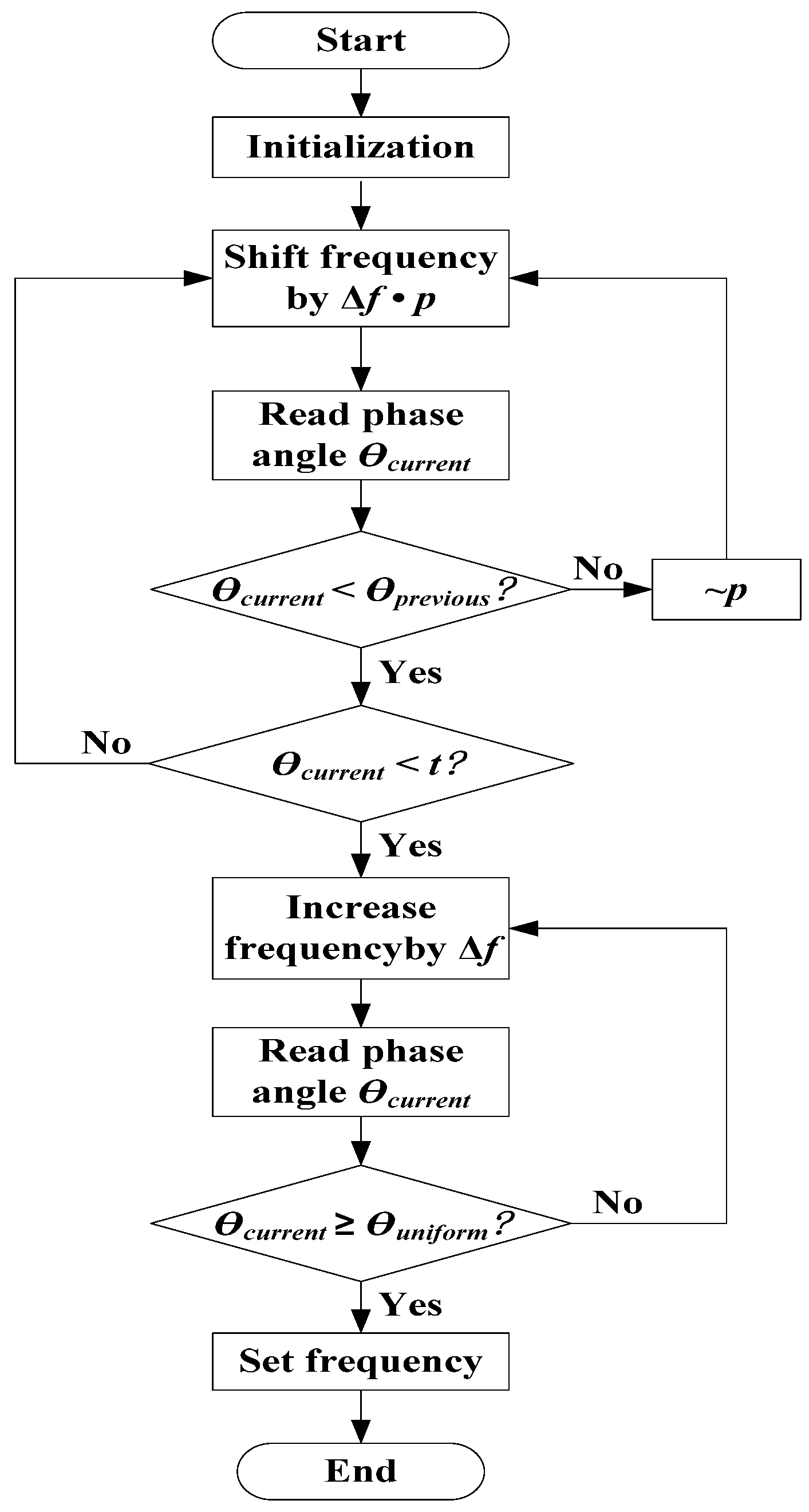
Firstly, the WPT system searches for the resonant frequency for a specific alignment condition. This resonant frequency is determined by the coil coupling, so it can be different each time a driver parks an EV. As shown in
Figure 5, the resonant frequency is located through frequency shifting (∆
fp) and phase angle comparison between current and previous angles (
θcurrent and
θprevious). As the polarity of the phase angle cannot be detected by the measurement circuit, a direction flag
p is utilized in the firmware to determine whether to shift the frequency to larger or smaller frequencies. The phase-angle which corresponds to the resonant frequency is zero, but the phase angle read by the DSP at the resonant frequency is not exactly zero due to the measurement error of digital devices. Therefore, the resonant frequency is set when the current phase angle (
θcurrent) is lower than
t, where
t is a value within the range of acceptable measurement accuracy. Secondly, the WPT system determines the uniform gain frequency once the resonant frequency is known. The tuning program increases the frequency step by step (∆
f) while measuring the load phase angle. The resonant frequency acquired in the first step determines the phase angle curve (
Figure 4b) and the mutual inductance between the two coils can be calculated according to Equation (1). Once the mutual inductance is known, the phase angle (
θuniform) for the uniform gain can be obtained using Equations (1) and (5). Then the DSP program increases the switching frequency step by step (∆
f) while measuring the load phase angle until the phase angle is equal to
θuniform. Finally, the WPT sets the switching frequency to the uniform gain frequency and raises the input DC voltage to begin charging the EV.
Figure 5.
Flowchart of the uniform voltage gain control loop.
Figure 5.
Flowchart of the uniform voltage gain control loop.
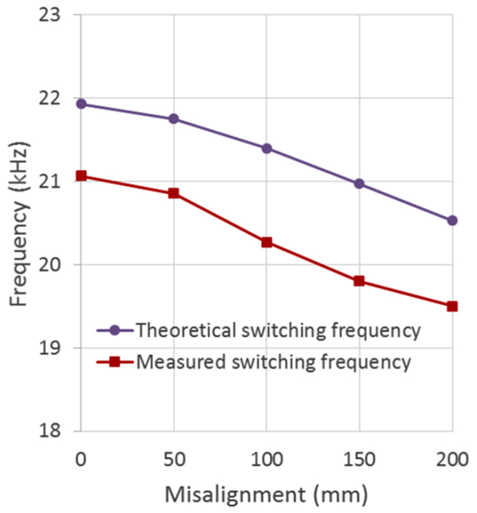
Theoretically, the calculation of the phase angle θuniform for a known coupling can be derived from Equations (1)–(5). However, a floating calculation could consume the computational resources of a 16-bit DSP dramatically and might influence the tuning speed as well. In addition, the theoretical value might have an error due to parasitic resistance and stray inductance in the electronic elements. Hence, the phase angle θuniform is calibrated for each increase (set 2 cm in our test) in misalignment and the coupling between two calibration points will linearly map the phase angle θuniform.


