Article

Numerical Validation of a New Approach to Model Single Junction Low Concentration PV Cells under Non-Uniform Illumination

1
Institute of Sustainable Energy Technology, Department of Architecture and Built Environment, University of Nottingham, University Park NG7 2RD, UK
2
Department of Architecture, University of Ferrara, Via Quartieri 8, Ferrara 44121, Italy
3
Department of Engineering, University of Ferrara, Via Saragat 1, Ferrara 44122, Italy
*
Authors to whom correspondence should be addressed.
Energies 2015, 8(5), 4529-4548; https://doi.org/10.3390/en8054529
Submission received: 28 February 2015 / Accepted: 11 May 2015 / Published: 20 May 2015

Abstract

:
This study presents a numerical validation of a new approach to model single junction PV cell under non-uniform illumination for low-concentration solar collectors such as compound parabolic concentrators (CPC). The simulation is achieved by finite element modelling (FEM). To characterize the results, the model is simulated with five different non-uniform illumination profiles. The results indicate that increasing the non-uniformity of concentrated light will introduce more resistive losses and lead to a significant attenuation in the PV cell short-circuit current. The FEM modelling results are then used to validate the array modelling approach, in which a single junction PV cell is considered equivalent to a parallel-connected array of several cell splits. A comparison between the FEM and array modelling approaches shows good agreement. Therefore, the array modelling approach is a fast way to investigate the PV cell performance under non-uniform illumination, while the FEM approach is useful in optimizing design of fingers and bus-bars on a PV.

1. Introduction

Increasing energy demands and environmental pollution have brought more attention on solar energy. It has many advantages, such as being pollution-free, safe, reliable and economically efficient [1,2]. The application of compound parabolic concentrating (CPC) technology offers the potential of increasing the electrical output by several-fold while using same number of PV cells [3]. A particular issue for CPC technology is the non-uniformity of illumination incident on the PV cell surface, which could cause hot spots, current mismatch and reduce the cell performance [4]. Understanding this issue and designing the cell appropriately could help to optimize cell efficiency.
The modelling of PV cells under worst scenario conditions has been studied for many years, any many good works have been reported. Tsai et al. [5] proposed an insolation-oriented model of PV modules using MATLAB, and explained the basic theory of PV modelling, Petrone et al. [6] built an analytical model of mismatched photovoltaics by means of the Lamber W-function, which uses mathematical techniques to predict PV cell performance under distributed light conditions. In most cases, the illumination distribution in a concentrated system is in either a Gaussian or anti-Gaussian distribution. Mellor et al. [7] proposed two dimensional finite element modelling (FEM) to simulate the front surface current flow in cells under non-uniform illumination and it explored new ideas for concentrated PV cell modelling. The simulation and experiment work done by Chemisana et al. [8] analyzed the electrical performance increase of concentrator solar cells under Gaussian temperature profiles. Baig et al. [9] carried out a comprehensive analysis of a concentrating photovoltaic (CPV) system through numerical modelling and experimental validation of a low photovoltaic system. The light distribution could be influenced by many factors, such as the shadowing from other components in the PV system. Wang et al. [10] proposed a simulation model to investigate the effects of the frame shadow on the PV characteristics in a photovoltaic/thermal system (PV/T) and their results shows the frame shadow could cause a 39.3% decrease in the photoelectric efficiency in the worst scenario. Vergura et al. [11] built a 3-D PV cell model by means of FEM which is able to represent the thermo-electrical behavior of PV cells under real conditions. In this model, the PV cell is formed by several layers and the software could simulate the cell from its physical properties. Domenech-Garret [12] also used a two dimensional finite element model to study the cell behavior under different combined Gaussian temperature and radiation profiles. It also takes into account several temperature amplitudes and the effect of movement of the illumination profiles across the cell. The experimental works of Hasan et al. [13] provide a comprehensive analysis of a building-integrated CPV system under real sky conditions. The variation of incident angles causes different non-uniform light distributions on the PV cell surface. The impact of non-uniformity of flux shows an average drop of 2.2% in the short-circuit current of a PV cell. Although, a lot of good works on PV cell modelling have been presented, it is still necessary to analyze cell performance in more detail for some specific purposes.
This study presents an FEM numerical validation of a new approach to modelling concentrating single junction PV cells under non-uniform illumination. The FEM model is built based on the extended mathematical expression for a single junction PV cell under non-uniform illumination and tested under five different non-uniform illumination profiles. In our previous study [14], an array modelling model has been proposed to simulate this situation, in which a concentrating single junction PV cell is represented by an equivalent array of several cell splits. Although the preliminary experimental verification has been conducted, it would be interesting to further validate this approach with the appropriate FEM results.

2. Materials and Methods

2.1. Model Domain

A single junction PV cell could be considered as a conductive medium consisting of three regions: emitter, bus bar and finger, as shown in Figure 1. The emitter region is a current source due to the release of electrons generated by the photons under illumination, leading to a voltage. The finger and bus bar region are solely conductive media to deliver electrons. In the FEM modelling, the PV cell would be represented as a collection of emitter, finger and bus bar. For the array modelling, the PV cell would be considered as an equivalent array of several identical split stripes, which is described in Section 3.3.
Figure 1. PV cell model domain.
Energies 08 04529 g001
The single junction silicon PV cell simulated in this study was intended for use with a trough shape miniature CPC, as shown in Figure 2, so it is a stripe with a single finger in the middle along the longitudinal direction of the PV cell. The PV stripe would be attached to the base of CPC, with its busbar at the end of the CPC.
Figure 2. Photo of a miniature solid CPC [15].
Energies 08 04529 g002

2.2. Mathematical Modelling

A simple equivalent circuit model for PV cell is given in Figure 3, which consists of a photo current, a diode, a parallel resistor expressing a leakage current and a series resistor describing an internal resistance to the current flow. The DC current flow in the circuit is expressed as follows:
I= I ph - I o [ exp ( V j n V T ) - 1 ] - V j R sh
where: V T = k B T/q ; V j =V+I R s .
Figure 3. PV cell equivalent circuit model [9].
Energies 08 04529 g003
Considering an illuminated PV cell, the term Iph is strongly dependent on the irradiance level and proportional to its intensity, the current generated from the emitter region of the cell is represented by Equation (2). The dark current in the finger and bus bar region as conductive media could be represented by Equation (3):
I e = I ph - I o [ exp ( V j n V T ) - 1 ] - V j R sh
I d = I o [ exp ( V j n V T ) - 1 ] - V j R sh
The incident light increases the temperature of the PV cell, which further increases the population of electrons exponentially enhancing the dark saturation current. This dependence of saturation current on the temperature is represented by Equation (4), which suggests that its value increases with temperature, but decreases with better material quality:
I o ( T ) = I oo T 3 exp [ - E go k B T ]
The term Ioo and Ego represent the saturation current and the band gap energy at 0 K and are both approximately constant with respect to temperature. Referencing to Mellor et al. [7], Equation (1) may be further be expressed as:
I = C 1 G + G 2 T 3 exp ( - T 1 T ) [exp( V j nV T )-1]+ C 3 V j
where: T 1 = E go /k B .
Based on above expression, Mellor et al. [7], proposed a continuity equation to determine the effective current density distribution of the PV cell surface under non-uniform illumination conditions. This governing equation solved over the solar cell domain is represented by:
× ( σ V J e ) = Q
In this study, the finite element method is applied to obtain the solution using the COMSOL Multi-Physics platform. The term V is the electric potential. The material conductivity σ is normally obtained experimentally, or it can be deduced from the material resistivity. Q represents the current source term in different regions; the current generated in the emitter region Qe and in the dark region Qd are expressed by:
Q e = C 1 G+C 2 T 3 exp( - E g kT )[exp( qV j nkT )- 1]+C 3 V j
Q d  = C C 2 T 3 exp( - E g kT )[exp( qV j nkT )- 1]+C 3 V
The terms C1, C2 and C3 are coefficients specific to a given cell, C1 is the photocurrent density per unit of incident power, C3 is the inverse of cell shunt resistance Rsh, and C2 is the saturation current density Jo at temperature To and could be expressed as follows [16]:
C 2 = J o T o 3 exp( - E g kT o )

2.3. Boundary Conditions

In the FEM model if the geometry and boundary condition are symmetric, then it is possible to reduce the geometry by half. In this simulation study, there are three types of boundary conditions: Interface condition:
- n b × (J 1 - J 2 ) = 0
Electric insulation:
n b × J = 0
Bus-bar electric potential:
V = V cell
where nb is the unit normal to the boundary, J1 and J2 are the current density vector at the boundary of adjacent media. J is the current density vector at the external boundary.
The interface condition is applied to all internal boundaries to ensure continuity of current at the interface between different media. The outside edges of the bus bars and external boundaries of the emitter section are electrically insulated. The ends of bus bars are connected to the external load and should therefore have electric potential equal to the cell operating voltage Vcell as an input parameter. All boundary conditions for FEM are shown in Figure 4. It may be useful to mention that the cell is actually a long stripe along the x-axis direction, but the scale ratio between x-axis and y-axis is adjusted to give a clearer view of the finger and bus-bar.
Figure 4. FEM boundary conditions, x-axis is the bus-bar direction (m) and y-axis is the finger direction (m).
Energies 08 04529 g004

2.4. Illumination Profiles under Boundary Conditions

The concentrated light through a CPC could be non-uniform according to the different incident angle. In most case, the distributed light may have a Gaussian distribution. The simulation is carried out under different illumination profiles. The model takes the x dependence of the light intensity incident on the cell, where x is perpendicular to the finger direction with the origin at the middle of the cell and this illumination expression is given as follows:
G(x) = G o A o exp( - x 2 2S o 2 )
Go is the mean illuminations across the cell area. So control the wide of Gaussian curve and related to the full width at half the maximum (FWHM) as:
FWHM = 2 2ln (2) S o
Ao is the normalization factor to ensure the mean irradiance across the PV cell is Go. Ao is equivalent to the ratio of peak to mean irradiance, where:
A o  =  W S o erf( W 2 2 S o )
W is the width of cell, and erf represents the error function and could be calculated by MATLAB.

2.5. Model Extension to Cell Level

To characterize the results obtained at the cell level and compare the difference between the different work schemes, we used some existing data from a previous work [14]. The selected cell domain was planned to work with a trough CPC with a long narrow design. The geometry of the cell domain is listed in Table 1.
Table 1. Model geometry.
ParameterValue
Emitter length0.160 m
Emitter width0.010 m
Bus-bar width0.011 m
Finger width0.001 m
The PV cell electric characteristics were obtained experimentally in our lab, under the standard test conditions (STC) of irradiance of 1000 W/m2, solar spectrum of AM 1.5 and module temperature at 25 °C [14], and are listed in Table 2. The cell coefficients are deduced from the cell electric characteristics and listed in Table 3. The electric conductivities for each region were adopted from [9], and are listed in Table 4. Those are boundary conditions inputs in the simulation.
Table 2. PV cell electric characteristics.
ParameterValue
Isc0.437 A
Voc0.429 V
Impp0.397 A
Vmpp0.337 V
Rs15.113 Ω
Rsh0.144 Ω
n0.5559
Table 3. PV Cell coefficients.
ParameterValue
C10.275 A·W−1
C2−52.86 Am−2·K−3
C3−3.156 Am−2·V−1
Table 4. Model boundary condition inputs.
ParameterValue
Emitter conductivity0.01 S/m
Bus-bar conductivity73.315 S/m
Finger conductivity27,200 S/m

3. Simulation Results and Discussion

3.1. Simulation of Non-Uniform Illumination Profiles

In this study, five different Gaussian distribution illumination profiles were considered according to the equations given in the previous section. In order to compare with uniform illumination conditions, all profiles have an average irradiance of 1000 W/m2. The input parameters for each profile are listed in Table 5, and the plots are shown in Figure 5.
Table 5. Parameters for each illumination profile.
ParameterProfile 1Profile 2Profile 3Profile 4Profile 5
FWHM (m)0.0550.0040.0030.00250.002
Ao1.91442.58663.44474.13355.1669
So0.00230.00170.00130.00110.000849
W (m)0.0110.0110.0110.0110.011
Go (W/m2)10001000100010001000
Figure 5. Illumination distribution over the cell for five illumination profiles, x-axis is the busbar direction (m).
Energies 08 04529 g005

3.2. Simulation Results for Comparison of Two Illumination Profiles

In this section, the FEM model uses Profile 3 in the simulation to investigate cell performance under non-uniform illumination conditions and compare them with uniform illumination conditions. The simulated illumination profiles are plotted in 
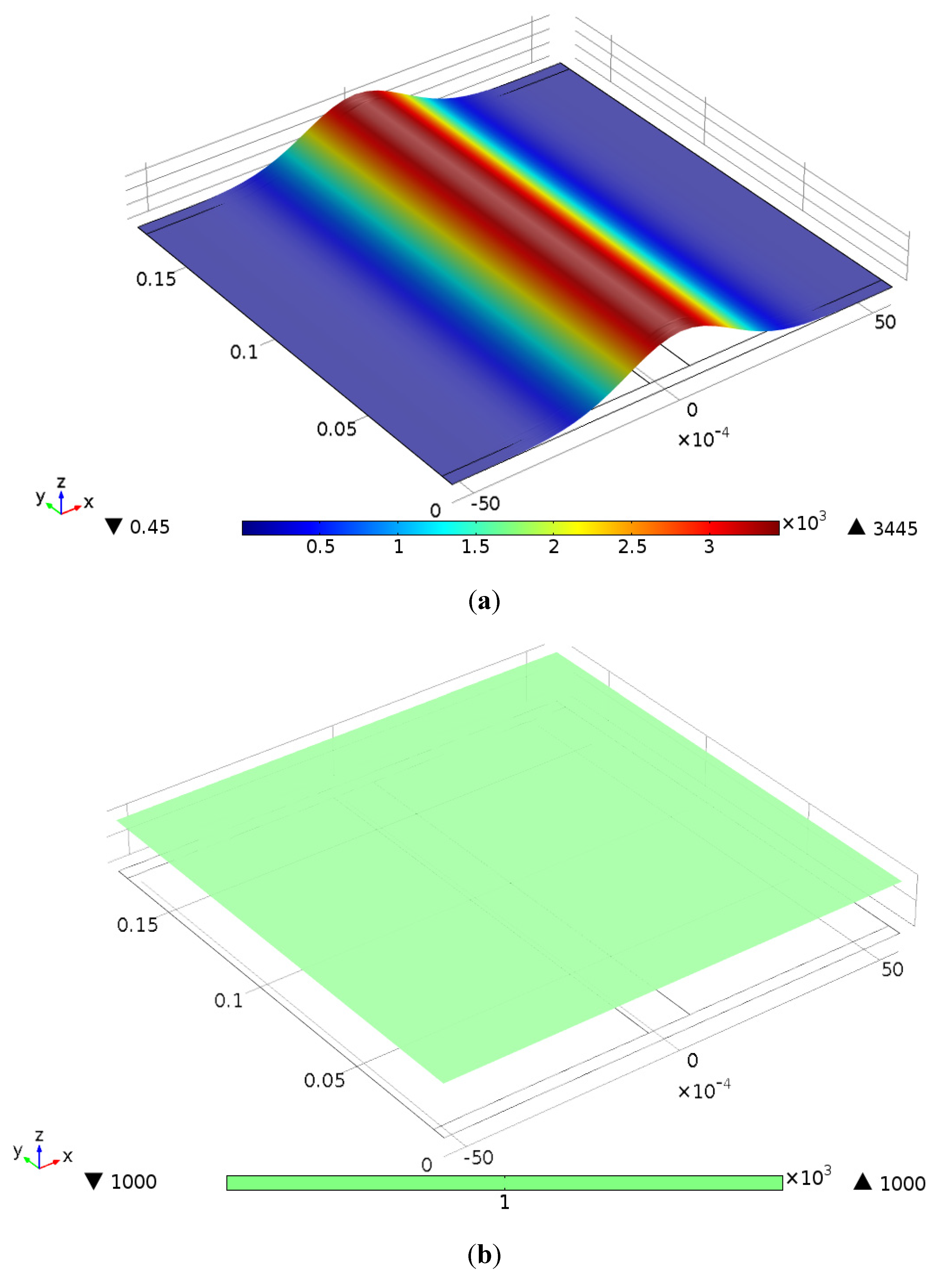
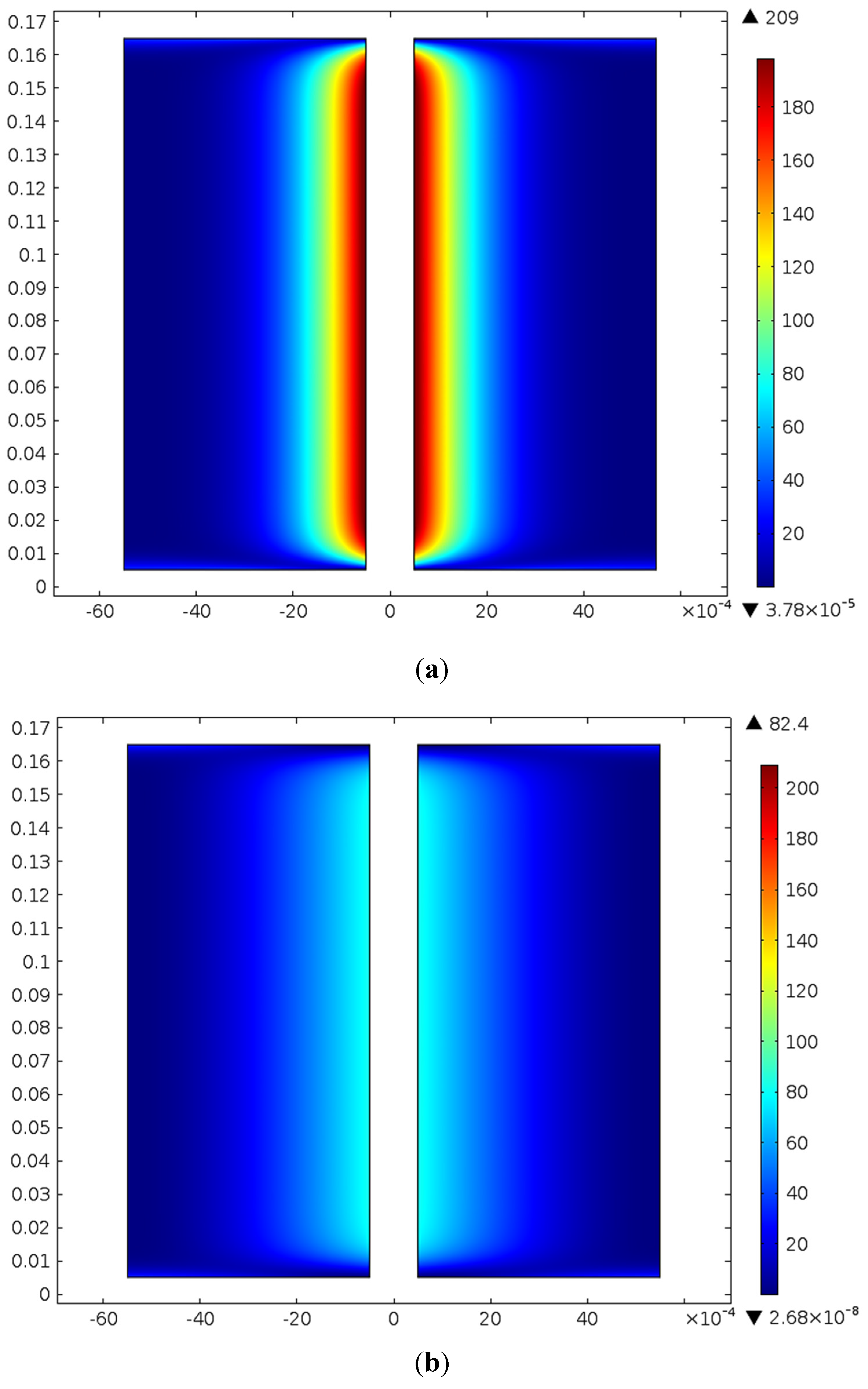
Figure 6. The Gaussian distribution illumination is distributed evenly along the cell longitudinal direction. The average illumination intensity per surface area is the same for both cases.
The voltage drop through the cell could be explained as a “distributed diode effect”, which could be summarized as follows: the lateral resistances in the cell lead to a voltage drop across the cell surface, causing different points on the cell surface to operate at different voltages and therefore produce different current densities, as explained by Franklin et al. [17]. The voltage distributions for both case are plotted in Figure 7. Under concentrated light conditions, the diode effect is significant since current densities could have large differences from the middle area towards to the edges and the resulting voltage drops are high.
Figure 6. Simulated illumination distribution for: (a) Profile 3; (b) Uniform illumination distribution, x-axis is the busbar direction (m) and y-axis is the finger direction (m).
Energies 08 04529 g006
Figure 7. PV cell surface voltage distribution under the short circuit condition for: (a) Profile 3; (b) uniform illumination distribution, x-axis is the bus bar direction (m) and y-axis is the finger direction (m).
Energies 08 04529 g007
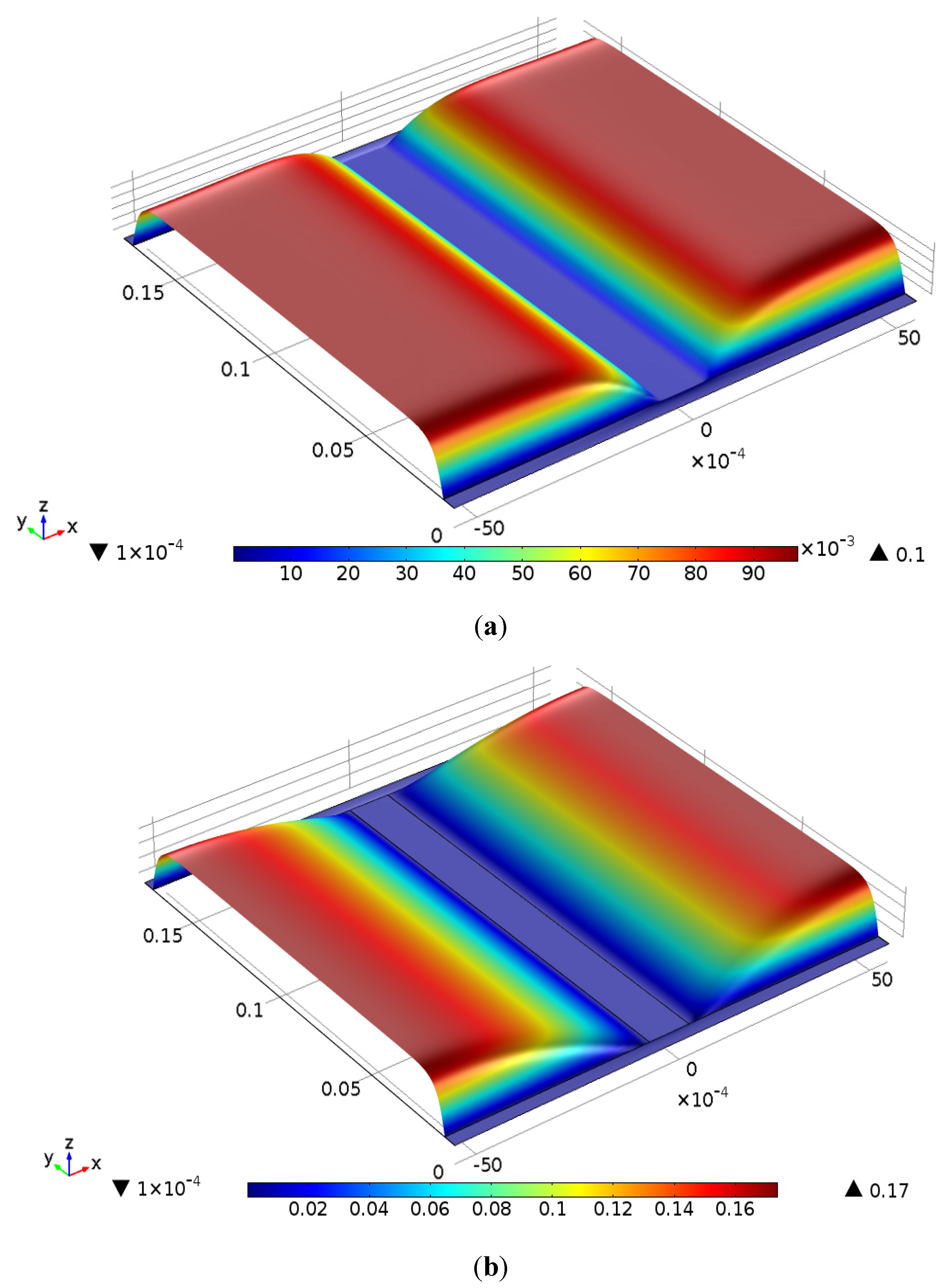
The cell surface current density distributions subjected to both conditions are given in 
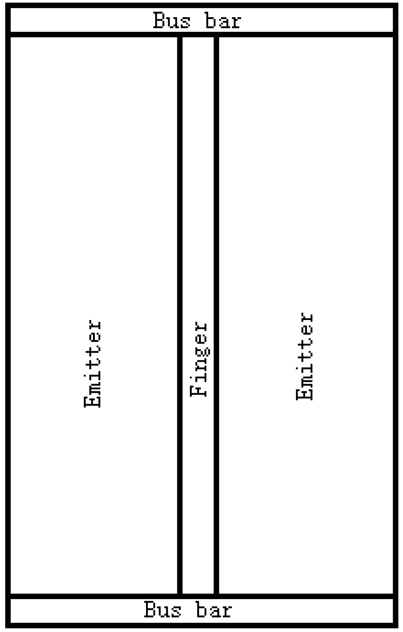
Figure 8. The high conductivity of the finger region will cause the generated current in emitter regions to be quickly absorbed and passed to the bus-bars. The high illumination area on the cell causes non-uniform current generation along the cell, which results in a sharping change of current density along the cell surface.
Figure 8. PV cell surface current density distribution under the short circuit condition for: (a) Profile 3; (b) uniform illumination distribution, x-axis is the bus-bar direction (m) and y-axis is the finger direction (m).
Energies 08 04529 g008
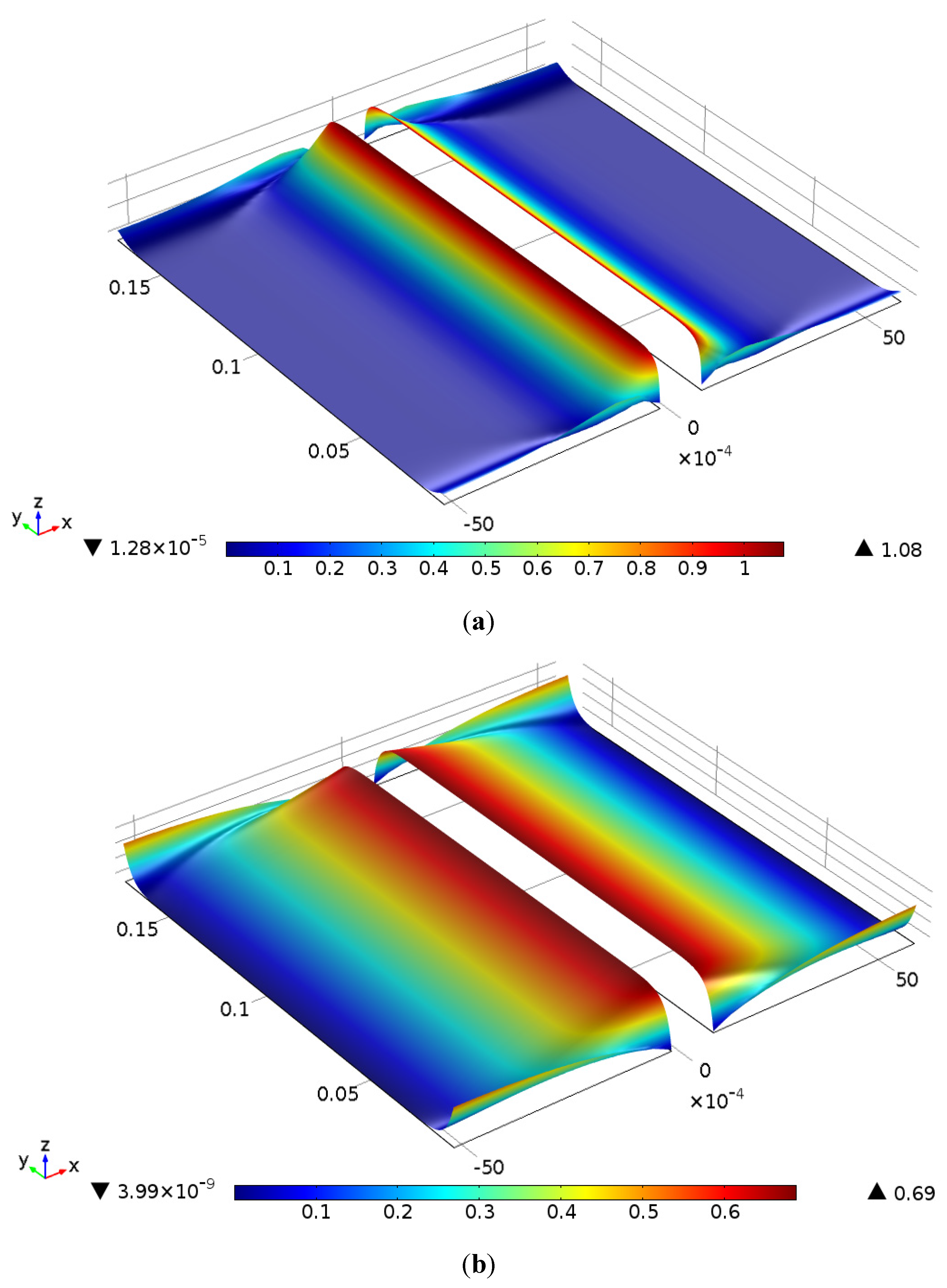
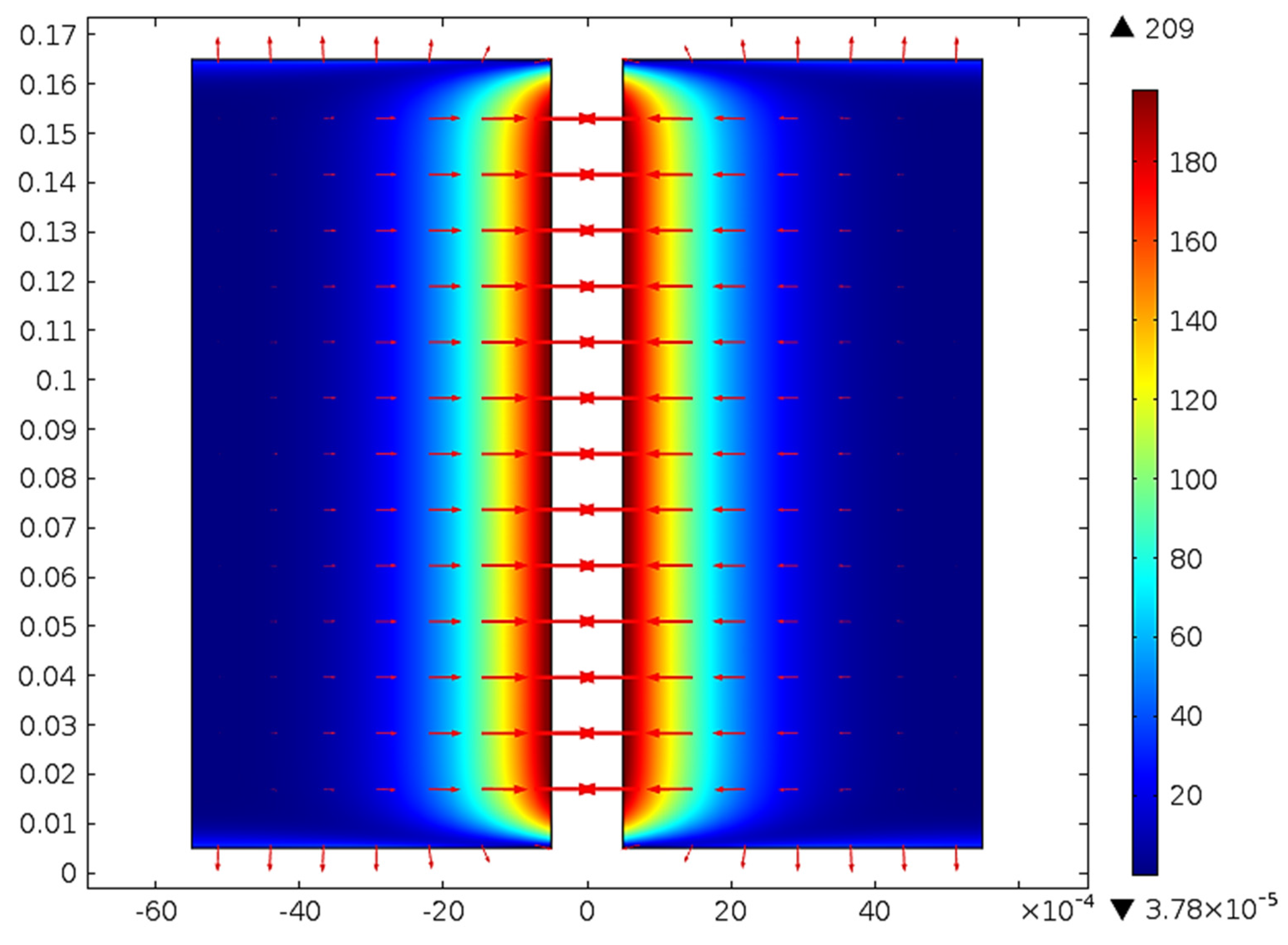
The biggest influence of non-uniform illumination is on the cell resistive losses. Both the position and intensity of the light play an important role to determine the resistive losses. Figure 9 shows a clear increase of resistive losses in the highly illuminated regions in comparison with uniform illumination conditions. This increase of resistive losses could be expressed in more detail by Figure 10, where the arrows indicate the direction and strength of the current. In the highly illuminated area, the generated photocurrent is absorbed by the finger region and then travels to the bus-bar, whereas, in the areas with less illumination, the generated current enters from the bus-bar and flows to the finger. The high non-uniformity makes the electrons to travel further through the finger to the bus-bars and causes the losses. A similar phenomenon is also mentioned in other works, such as Franklin et al. [17].
Figure 9. PV cell surface resistive losses distribution under the short circuit condition for: (a) Profile 3 (b) uniform illumination distribution, x-axis is the bus-bar direction (m) and y-axis is the finger direction (m).
Energies 08 04529 g009
Figure 10. PV cell surface resistive losses distribution and vector of current for Profile 3 under the short circuit condition, x-axis is the bus-bar direction (m) and y-axis is the finger direction (m).
Energies 08 04529 g010
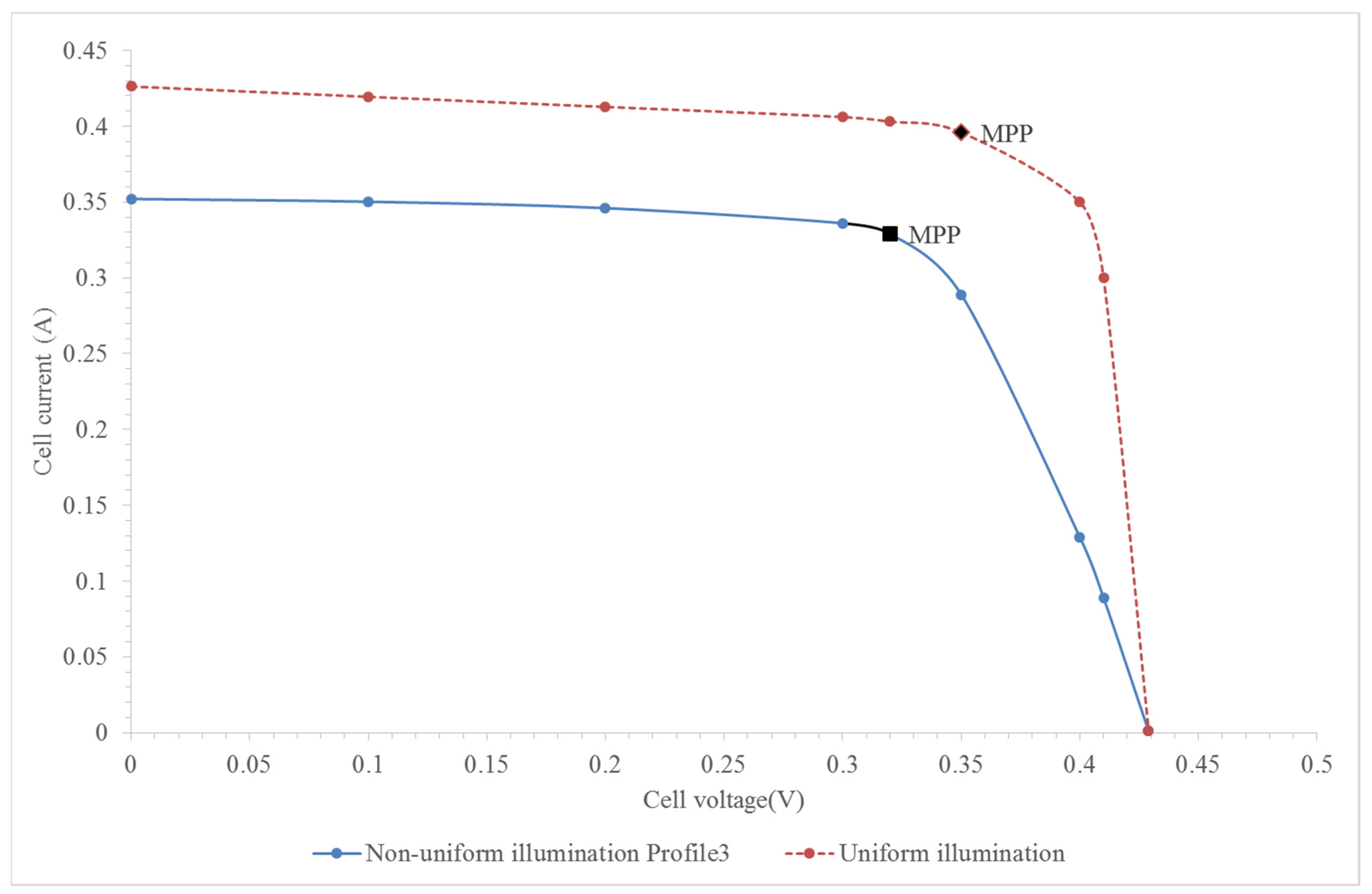
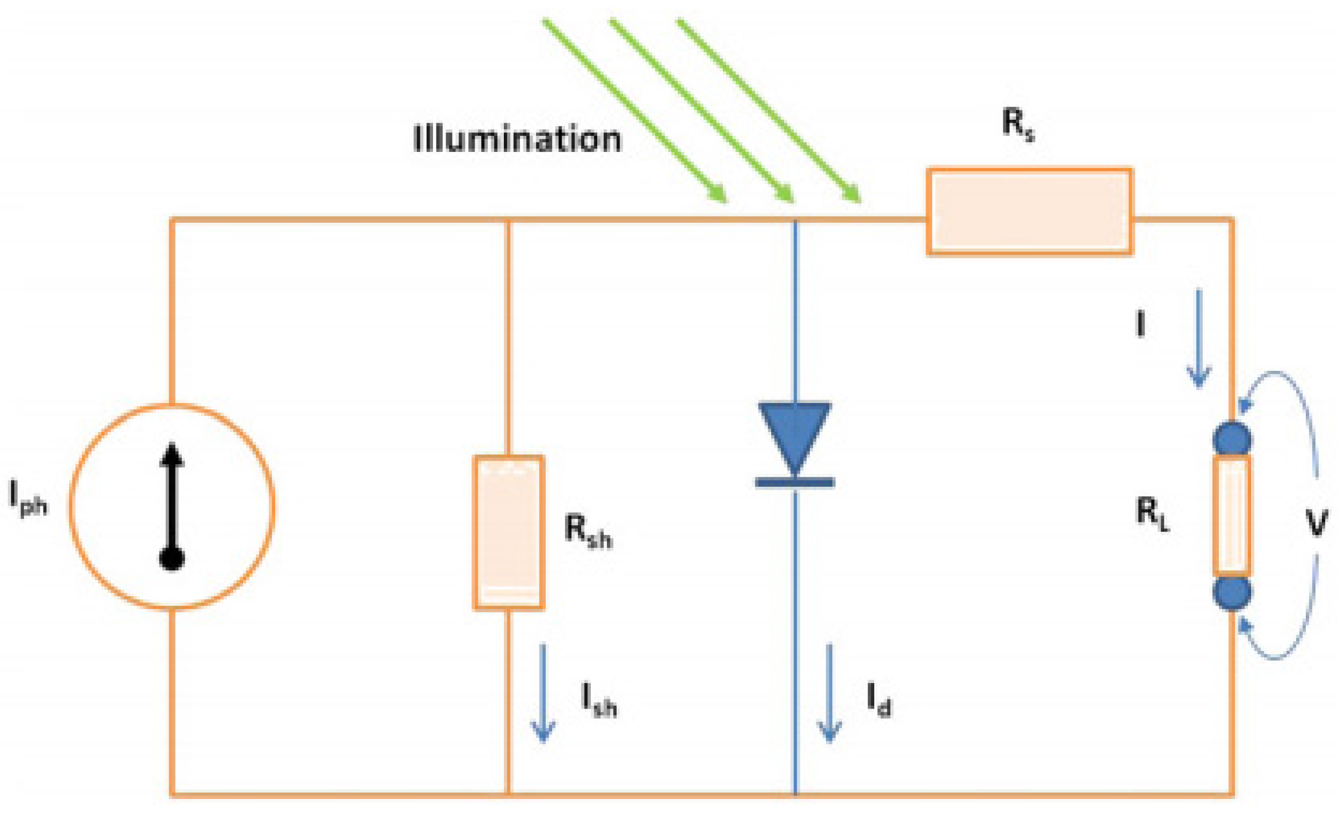
Usually an I-V curve is used to demonstrate the performance of the PV cell and can be generated by the superposition of the cell diode I-V curve in the dark with light-generated current. For a given boundary voltage, the current of a PV cell can be obtained from the FEM results, and the plot I-V curves can be then given. Figure 11 shows the simulation results of PV cell performance under both uniform light and non-uniform light conditions. In this simulation, the cell operating temperature is considered as a constant. Since the voltages are mostly influenced by varying temperature, the voltages in both saturations are constant. The high resistive losses introduced by non-uniform illumination cause the maximum current to drop significantly. The maximum power point would also shift from this influence, which gives about a 20% drop in the cell efficiency. It may be necessary to mention that this drop also includes the effect of finger shading, which is discussed in the following section.

3.3. Comparison between FEM and Array Modelling

The array modelling is a different approach to investigate PV cell performance under non-uniform illumination. It simply considers the cell to be equivalent to a parallel-connected array of numerous small cell splits, where each split has its own input parameters according to the illumination profile. The final output is the combination from each split. The array modelling is implemented on the MATLAB platform and built mostly on the mathematical expressions. However, the FEM has more features to analyze the physical properties of PV cell, while the array modeling is a fast approach to produce I-V curves because it is based on algebraic calculations. The aim is to compare both approaches in order to investigate a more efficient way to simulate PV cell under non-uniform illumination condition. The detail about the array modelling can be found in our previous study [14].
Figure 11. I-V curves for uniform illumination and illumination Profile 3.
Energies 08 04529 g011
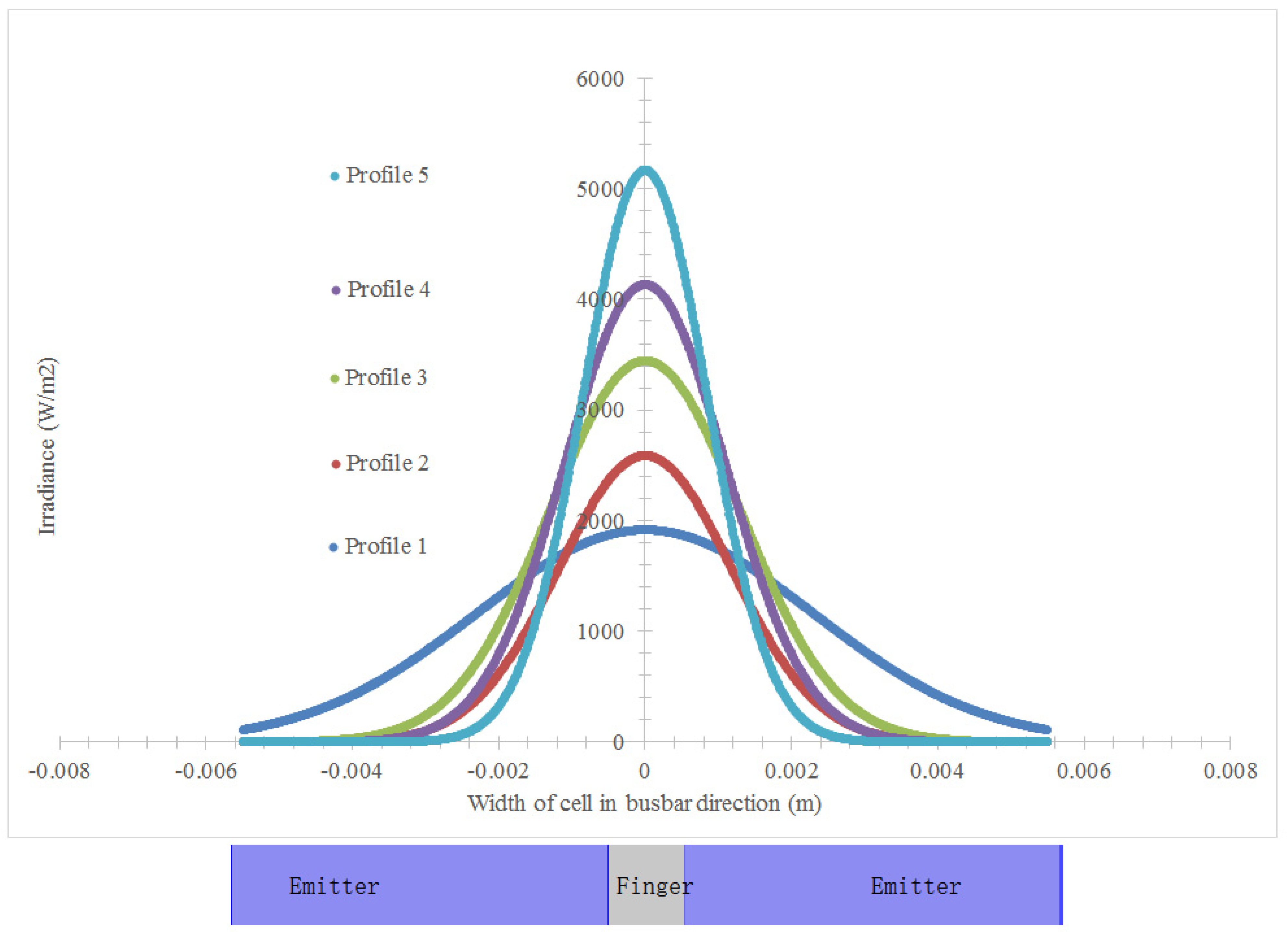
The illumination profiles simulated in the array modelling were given according to the distributions in Figure 5 and listed in Table 6, in order to characterize the results obtained from both approaches. The cell is assumed to be split evenly into 10 stripes to give 0.001 m (1 mm) width each cell split. For the y-axis direction in Figure 4, the illumination is assumed to be uniform. The average irradiance value was calculated according to the distribution along the x-axis over the 0.001 m width for each cell split. However, as the non-uniformity increases, more light is concentrated in the middle region and sharply drops towards the edges along the x-axis direction in Figure 4. For all of the illumination profiles, a significant portion of light is shaded by the finger, therefore the shading from the finger needs to be considered in the array modelling. The finger width is 0.001 m, which means half of Split 5 and Split 6 are shaded. Therefore, the range of the illumination distribution to estimate the irradiance value is from −0.001 to −0.0005 for Split 5 and from 0.0005 to 0.001 for Split 6. The reason for this adjustment is because the array modelling is not related to the structure of a cell, but just the overall performance of a cell. To count the effect of the width of the finger in the array modelling and have a fair comparison with the FEM approach, the above adjustment was therefore made to each illumination profile including uniform distribution.
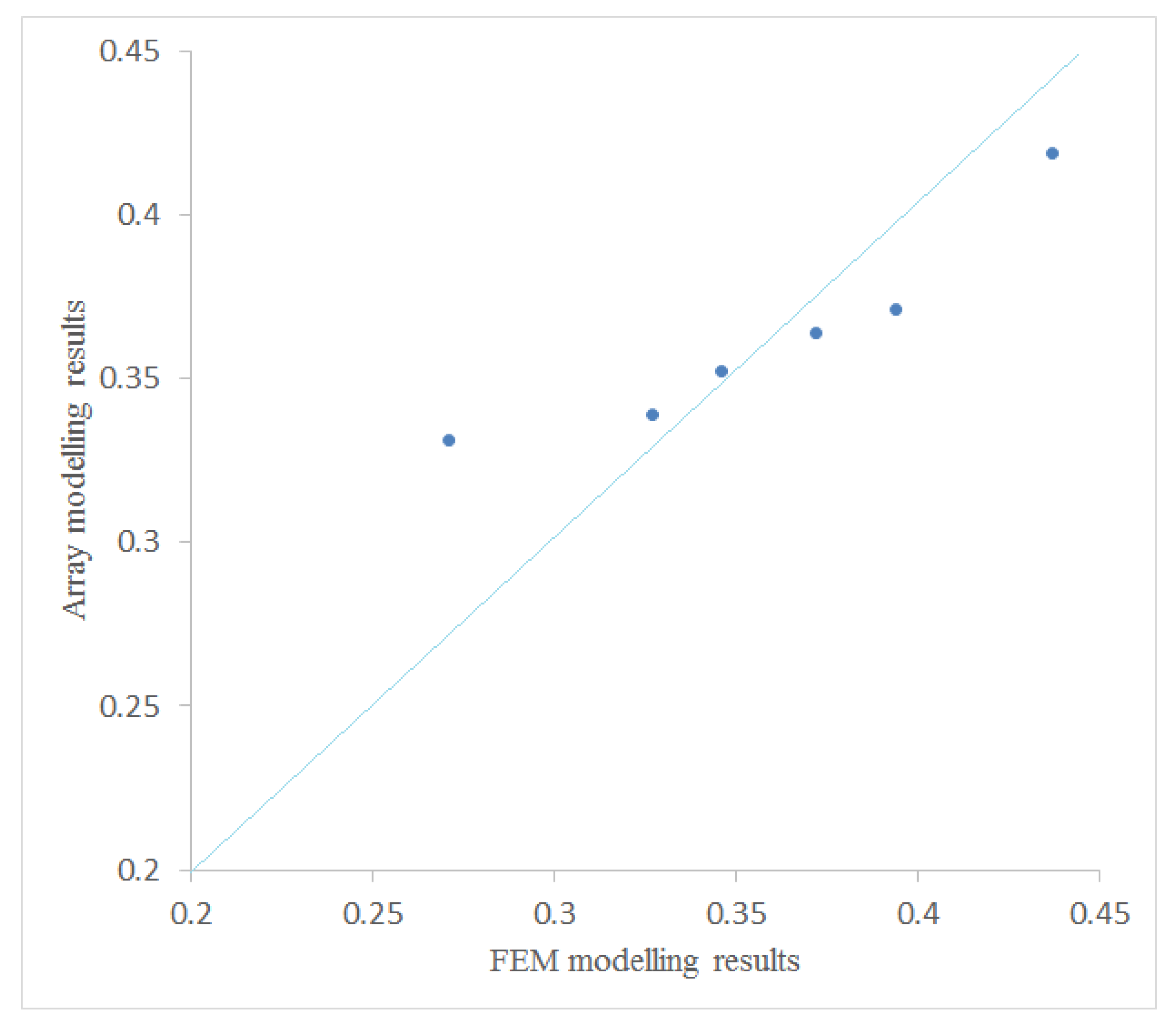
The high non-uniformity introduces more resistive losses and causes the decrease of the maximum current output. The simulation results for short-circuit current were obtained from two modelling approaches and listed in Table 7. The results from both platforms show a good agreement, as can be seen from Figure 12. The relative deviations are mostly within ±10%, however it becomes larger when the non-uniformity of illumination is bigger.
Table 6. Irradiance values for ten cell splits in the array modelling (W/m2).
ProfileSplit 1Split 2Split 3Split 4Split 5Split 6Split 7Split 8Split 9Split 10Average
Uniform10001000100010005005001000100010001000900
Profile 137457798014069029021406980577374848
Profile 292352891167611611161167689135292834
Profile 3110568818001440144018006881051807
Profile 415045017651620162017654505011777
Profile 51111411321173017301321134111760
Table 7. Simulation results of short-circuit current in two modelling approaches.
ProfileFinite element modelling (A)Array modelling (A)Relative deviation (%)
Uniform0.4370.419−4
Profile 10.3940.371−6
Profile 20.3720.364−2
Profile 30.3460.3522
Profile 40.3270.3394
Profile 50.2710.33118
Figure 12. Simulation results from two modelling approaches.
Energies 08 04529 g012
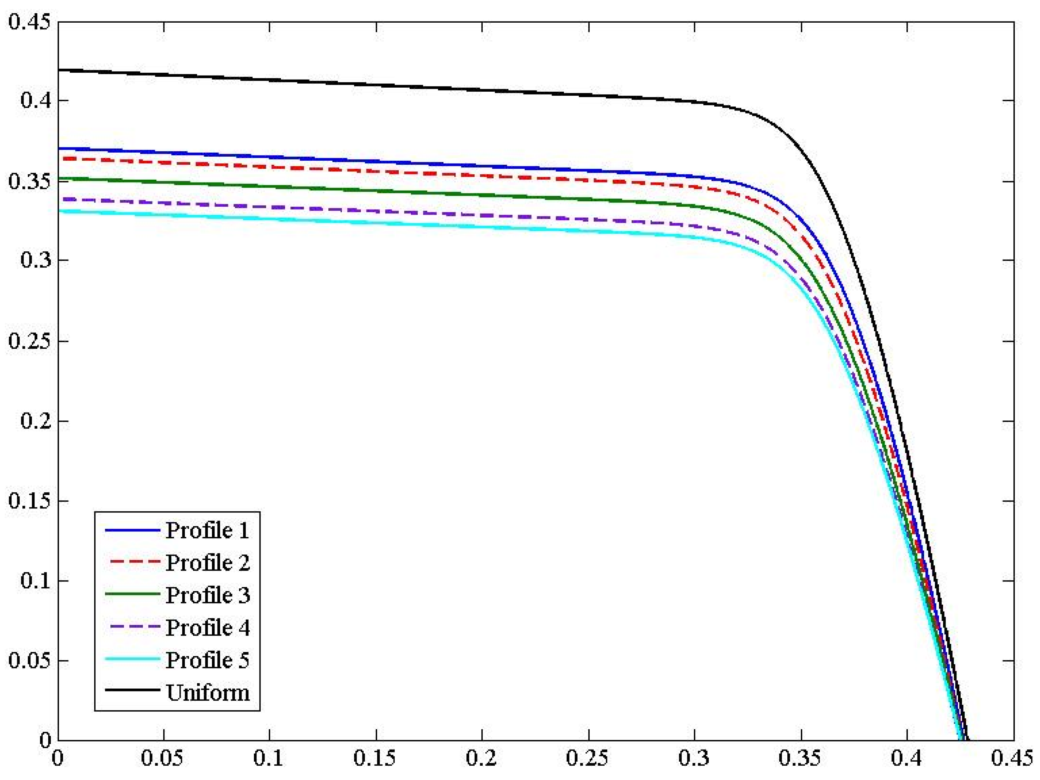
The I-V curves for each illumination profile in the array modelling are plotted in Figure 13. From Profiles 1 to 5, it can see the drop in short-circuit current as well as shifting of the maximum power point. Besides the influence from non-uniform illumination, the cell efficiency could also be affected by the finger design. This indicates the importance of finger design and positioning. 
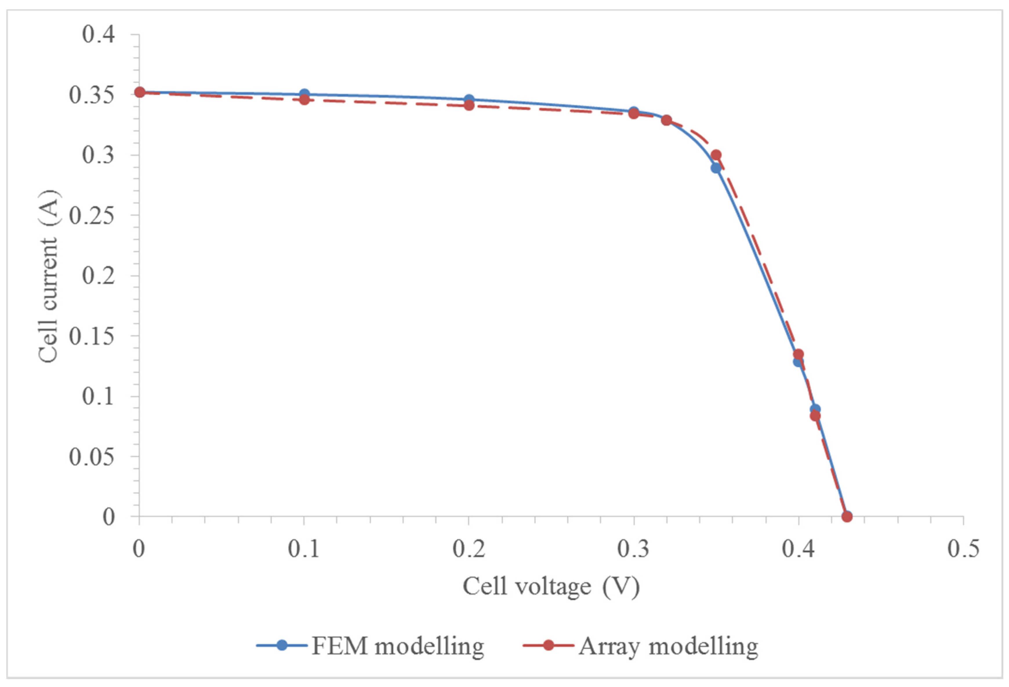
Figure 14 gives the I-V curves and maximum power points for illumination Profile 3 for both approaches, and indicates a good agreement between them. In the FEM approach, the geometry design can be easily changed according to the requirements, so it can offer an appropriate way for designing and positioning fingers, while the array modelling approach may represent a fast way to investigate the effect of non-uniform illumination, for example, by plotting I-V curves.
Figure 13. I-V curves given by the MATLAB array modelling for several illumination profiles.
Energies 08 04529 g013
Figure 14. I-V curves given by array modelling and FEM modelling for illumination Profile 3.
Energies 08 04529 g014

4. Conclusions

This study has presented the finite element modelling (FEM) of a single junction low concentration PV cell, with the purpose of validating a new approach to model concentrating single junction PV cells under non-uniform illumination, in which a PV cell is considered equivalent to a parallel-connected array of several cell splits. The FEM model has been built based on the extended mathematical expression for single junction low concentration PV cells under non-uniform illumination and tested under five different non-uniform illumination profiles. The PV cell surface voltage, current density distribution and resistive losses for both uniform illumination and non-uniform illumination conditions have been simulated. The results indicate that increasing non-uniformity of the concentrated light would introduce more resistive losses and lead to a significant attenuation in the PV cell short-circuit current. A comparison between the FEM and the array modelling approaches has been given. The two modelling approaches are compared for the same illumination profiles and their results show good agreement when the shading effect of fingers is taken into account. It was found in the FEM approach that the finger design and positioning could have great influence on PV cell performance, especially in high non-uniform conditions. From this point of view, the FEM approach has more potential in future simulation work, since it is a physical model and it is easier to modify the cell geometry, in comparison with the array modelling, which offers a fast way to produce I-V curves of single junction low concentration PV cells under non-uniform illumination conditions.

Acknowledgments

Thanks to European Commission for a Marie Curie Fellowship grant (PIIF-GA-2009-253945). The authors would also like to thank the University of Ferrara for their financial support (Young Researchers Funds 2014, International Research Funds 2014).

Author Contributions

Hang Zhou has conducted the simulation study and prepared the draft manuscript. Yuehong Su has proposed the topic, supervised this study and revised the manuscript. Michele Bottarelli and Marco Bortoloni have discussed about the idea, offered a great support for simulation and also revised the manuscript. Shenyi Wu has helped with FEM simulation.

Nomenclature

SymbolUnitDescription
IAPV cell generated current
IeACurrent generated in illuminated region
IphAPhoto-generated current
IdADark current in dark region
IoAReverse saturation current
VVPV cell voltage across external load
VTVThermodynamic voltage
VjVJunction voltage
RLΩExternal load resistance
RshΩShunt resistancee
RsΩSeries resistance
kBJ/KBoltzmann constant
qCElectron charge
n Diode ideal factor
JeA/m2Current density
QjA/m2Generated current density
σS/mConductivity of material
RsheetΩSheet resistance
Rp.u.lΩ/mResistance per unit length
QeA/m2Current density generated in emitter region
QdA/m2Current density generated in dark region
GW/m2Illumination profile
TKPV cell working temperature
EgeVMaterial band-gap energy (1.124 eV for silicon)

Conflicts of Interest

The authors declare no conflict of interest.

References

  1. Noam, L. Sustainable energy development: The present. Situation and possible paths to the future. Energy 2011, 43, 174–191. [Google Scholar]
  2. Ibrahim, A.; Othman, M.Y.; Ruslan, M.H.; Mat, S.; Sopian, K. Recent advances in flat plate photovoltaic/thermal (PV/T) solar collectors. Renew. Sustain. Energy Rev. 2011, 15, 352–365. [Google Scholar] [CrossRef]
  3. Tao, T.; Zheng, H.; Su, Y.; Riffat, S.B. A novel combined solar concentration/wind augmentation system: Constructions and preliminary testing of a prototype. Appl. Therm. Eng. 2011, 31, 3664–3668. [Google Scholar] [CrossRef]
  4. Li, G.; Pei, G.; Su, Y.; Ji, J.; Saffa, B.R. Experiment and simulation study on the flux distribution of lens-walled compound parabolic concentrator compared with mirror compound parabolic concentrator. Energy 2013, 58, 398–403. [Google Scholar] [CrossRef]
  5. Tsai, H.-L. Insolation-oriented model of photovoltaic moduleusing MATLAB/SIMULINK. Sol. Energy 2010, 84, 1318–1326. [Google Scholar] [CrossRef]
  6. Petrone, G.; Spagnulo, G.; Vitelli, M. Analytical model of mismatched photovoltaic fields by means of Lambert W-function. Sol. Energy Mater. Sol. Cells 2007, 91, 1652–1657. [Google Scholar] [CrossRef]
  7. Mellor, A.; Domenech-Garret, J.L.; Chemisana, D.; Rosell, J.I. A two-dimensional finite element model of front surface current flow in cells under nonuniform, concentrated illumination. Sol. Energy 2009, 83, 1459–1465. [Google Scholar] [CrossRef] [Green Version]
  8. Chemisana, D.; Rosell, J.I. Electrical performance increase of concentrator solar cells under Gaussian temperature profiles. Prog. Photovolt. Res. Appl. 2013, 21, 444–455. [Google Scholar]
  9. Hasan, B.; Nabin, S.; Keith, C.H.; Tapas, K.M. Numerical modelling and experimental validation of a low concentrating photovoltaic system. Sol. Energy Mater. Sol. Cells 2013, 113, 201–219. [Google Scholar] [CrossRef]
  10. Wang, Y.; Pei, G.; Zhang, L. Effect of frame shadow on the PV character of a photovoltaic/thermal system. Appl. Energy 2014, 130, 326–332. [Google Scholar] [CrossRef]
  11. Vergura, S.; Acciani, G.; Falcone, O. 3-D PV-cell model by means of FEM. In Proceedings of the International Conference on Clean Electrical Power (ICCEP), Capri, Italy, 9–11 June 2009; pp. 35–40.
  12. Domenech-Garret, J.L. Cell behavior under different non-uniform temperature and radiation combined profiles using a two dimensional finite element model. Sol. Energy 2011, 85, 256–264. [Google Scholar] [CrossRef]
  13. Hasan, B.; Nazmi, S.; Daniel, C.; Joan, R.; Tapas, K.M. Performance analysis of dielectric based 3D building integrated concentrating photovoltaic system. Sol. Energy 2014, 103, 525–540. [Google Scholar] [CrossRef]
  14. Zhou, H.; Su, Y.; Pei, G.; Wang, Y. A new approach to model concentrating PV cells under non-uniform illumination. Energy Res. J. 2015, in press. [Google Scholar]
  15. Yu, X.; Su, Y.; Zheng, H.; Riffat, S. A study on use of miniature dielectric compound parabolic concentrator (dCPC) for daylighting control application. Build. Environ. 2014, 74, 75–85. [Google Scholar] [CrossRef]
  16. Rosell, J.I.; Ibanez, M. Modelling power output in photovoltaic modules for outdoor operating conditions. Energy Convers. Manag. 2006, 47, 2424–2430. [Google Scholar] [CrossRef]
  17. Franklin, E.; Coventry, J. Effects of highly non-uniform illumination distribution on electrical performance of solar cells. In Proceedings of the 40th annual conference for the Australian New Zealand Solar Energy Society, Newcastle, Australia, 27–30 November 2002.

